February 1984
Revised February 1999
MM74HCT540
∑ MM74HCT541
In
ver
ti
ng Oct
a
l
3-
S
T
A
T
E Buf
f
e
r
∑
Octal
3
-
ST
A
T
E
Buff
er
© 1999 Fairchild Semiconductor Corporation
DS006040.prf
www.fairchildsemi.com
MM74HCT540 ∑ MM74HCT541
Inverting Octal 3-STATE Buffer ∑ Octal 3-STATE Buffer
General Description
The MM74HCT540 and MM74HCT541 3-STATE buffers
utilize advanced silicon-gate CMOS technology and are
general purpose high speed inverting and non-inverting
buffers. They possess high drive current outputs which
enable high speed operation even when driving large bus
capacitances. These circuits achieve speeds comparable
to low power Schottky devices, while retaining the low
power consumption of CMOS. Both devices are TTL input
compatible and have a fanout of 15 LS-TTL equivalent
inputs.
MM74HCT devices are intended to interface between TTL
and NMOS components and standard CMOS devices.
These parts are also plug-in replacements for LS-TTL
devices and can be used to reduce power consumption in
existing designs.
The MM74HCT540 is an inverting buffer and the
MM74HCT541 is a non-inverting buffer. The 3-STATE con-
trol gate operates as a two-input NOR such that if either G1
or G2 are HIGH, all eight outputs are in the high-imped-
ance state.
In order to enhance PC board layout, the MM74HCT540
and MM74HCT541 offers a pinout having inputs and out-
puts on opposite sides of the package. All inputs are pro-
tected from damage due to static discharge by diodes to
V
CC
and ground.
Features
s
TTL input compatible
s
Typical propagation delay: 12 ns
s
3-STATE outputs for connection to system buses
s
Low quiescent current: 80
µ
A
s
Output current: 6 mA (min.)
Ordering Code:
Devices also available in Tape and Reel. Specify by appending the suffix letter "X" to the ordering code.
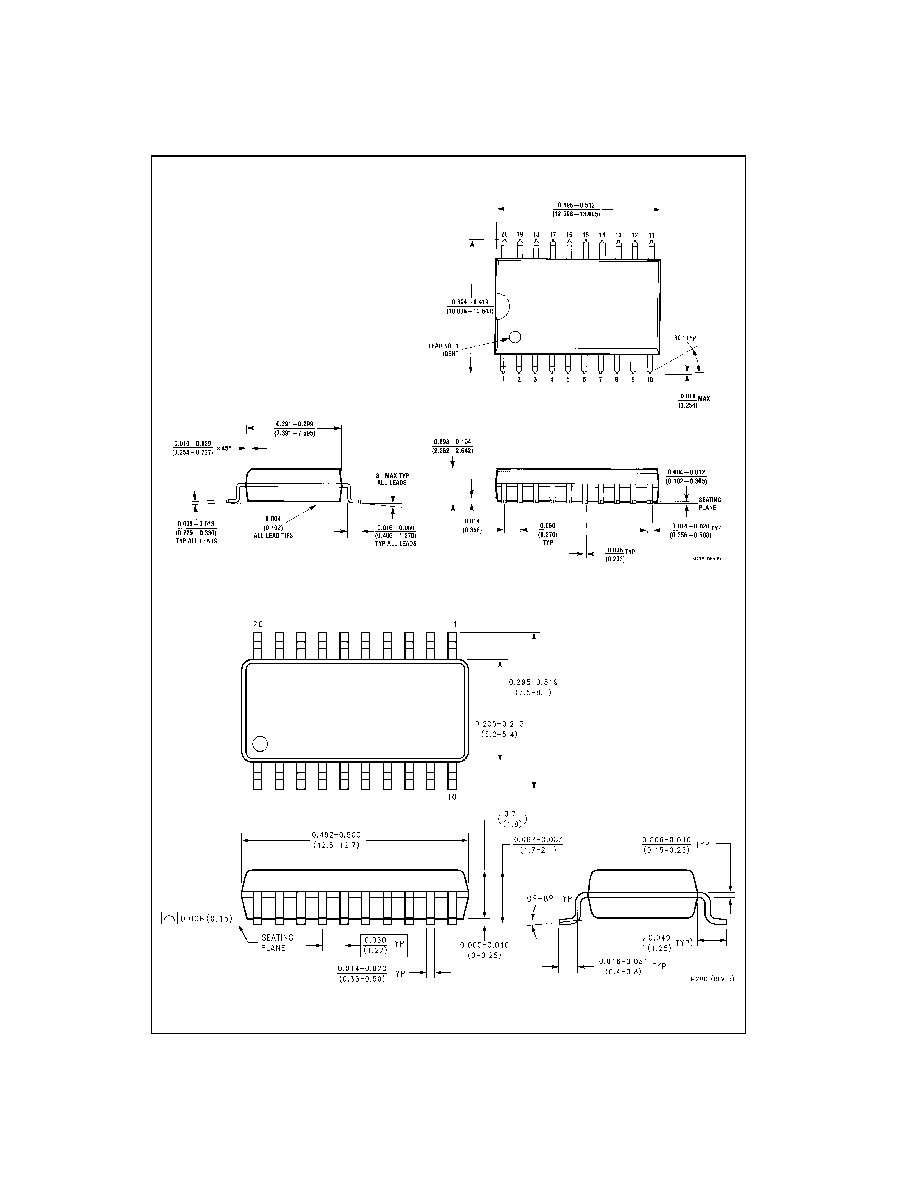
Connection Diagrams
Pin Assignments for DIP, SOIC, SOP and TSSOP
Top View
MM74HCT540
Top View
MM74HCT541
Order Number
Package Number
Package Description
MM74HCT540WM
M20B
20-Lead Small Outline Integrated Circuit (SOIC), JEDEC MS-013, 0.300" Wide
MM74HCT540SJ
M20D
20-Lead Small Outline Package (SOP), EIAJ TYPE II, 5.3mm Wide
MM74HCT540MTC
MTC20
20-Lead Thin Shrink Small Outline Package (TSSOP), JEDEC MO-153, 4.4mm Wide
MM74HCT540N
N20A
20-Lead Plastic Dual-In-Line Package (PDIP), JEDEC MS-001, 0.300" Wide
MM74HCT541WM
M20B
20-Lead Small Outline Integrated Circuit (SOIC), JEDEC MS-013, 0.300" Wide
MM74HCT541SJ
M20D
20-Lead Small Outline Package (SOP), EIAJ TYPE II, 5.3mm Wide
MM74HCT541MTC
MTC20
20-Lead Thin Shrink Small Outline Package (TSSOP), JEDEC MO-153, 4.4mm Wide
MM74HCT541N
N20A
20-Lead Plastic Dual-In-Line Package (PDIP), JEDEC MS-001, 0.300" Wide
www.fairchildsemi.com
2
MM
74
H
C
T5
40
∑ MM
74HCT541
Absolute Maximum Ratings
(Note 1)
(Note 2)
Recommended Operating
Conditions
Note 1: Absolute Maximum Ratings are those values beyond which dam-
age to the device may occur.
Note 2: Unless otherwise specified all voltages are referenced to ground.
Note 3: Power Dissipation temperature derating -- plastic "N" package:
-
12 mW/
∞
C from 65
∞
C to 85
∞
C.
DC Electrical Characteristics
V
CC
=
5V
±
10% (unless otherwise specified)
Note 4: Measured per input. All other inputs at V
CC
or GND.
Supply Voltage (V
CC
)
-
0.5 to
+
7.0V
DC Input Voltage (V
IN
)
-
1.5 to V
CC
+
1.5V
DC Output Voltage (V
OUT
)
-
0.5 to V
CC
+
0.5V
Clamp Diode Current (I
IK
, I
OK
)
±
20 mA
DC Output Current, per pin (I
OUT
)
±
35 mA
DC V
CC
or GND Current, per pin (I
CC
)
±
70 mA
Storage Temperature Range (T
STG
)
-
65
∞
C to
+
150
∞
C
Power Dissipation (P
D
)
(Note 3)
600 mW
S.O. Package only
500 mW
Lead Temperature (T
L
)
(Soldering 10 seconds)
260
∞
C
Min
Max
Units
Supply Voltage (V
CC
)
4.5
5.5
V
DC Input or Output Voltage
(V
IN
, V
OUT
)
0
V
CC
V
Operating Temperature Range (T
A
)
-
40
+
85
∞
C
Input Rise or Fall Times
(t
r
, t
f
)
500
ns
Symbol
Parameter
Conditions
T
A
=
25
∞
C
T
A
=
-
40 to 85
∞
C T
A
=
-
55 to 125
∞
C
Units
Typ
Guaranteed Limits
V
IH
Minimum HIGH Level
2.0
2.0
2.0
V
Input Voltage
V
IL
Maximum LOW Level
0.8
0.8
0.8
V
Input Voltage
V
OH
Minimum HIGH Level
V
IN
=
V
IH
or V
IL
Output Voltage
|I
OUT
|
=
20
µ
A
V
CC
V
CC
-
0.1
V
CC
-
0.1
V
CC
-
0.1
V
|I
OUT
|
=
6.0 mA, V
CC
=
4.5V
4.2
3.98
3.84
3.7
V
|I
OUT
|
=
7.2 mA, V
CC
=
5.5V
5.2
4.98
4.84
4.7
V
V
OL
Maximum LOW Level
V
IN
=
V
IH
or V
IL
Voltage
|I
OUT
|
=
20
µ
A
0
0.1
0.1
0.1
V
|I
OUT
|
=
6.0 mA, V
CC
=
4.5V
0.2
0.26
0.33
0.4
V
|I
OUT
|
=
7.2 mA, V
CC
=
5.5V
0.2
0.26
0.33
0.4
V
I
IN
Maximum Input
V
IN
=
V
CC
or GND
±
0.1
±
1.0
±
1.0
µ
A
Current
I
OZ
Maximum 3-STATE
V
OUT
=
V
CC
or GND
±
0.5
±
5.0
±
10
µ
A
Output Leakage
G
=
V
IH
Current
I
CC
Maximum Quiescent
V
IN
=
V
CC
or GND
8.0
80
160
µ
A
Supply Current
I
OUT
=
0
µ
A
V
IN
=
2.4V or 0.5V (Note 4)
0.6
1.0
1.3
1.5
mA

3
www.fairchildsemi.com
MM74HCT540
∑ MM74HCT541
AC Electrical Characteristics
MM74HCT540: V
CC
=
5.0V, t
r
=
t
f
=
6 ns, T
A
=
25
∞
C, (unless otherwise specified)
AC Electrical Characteristics
MM74HCT540: V
CC
=
5.0V
±
10%, t
r
=
t
f
=
6 ns (unless otherwise specified)
Note 5: C
PD
determines the no load dynamic power consumption, P
D
=
C
PD
V
CC
2 f
+
I
CC
V
CC
,and the no load dynamic current consumption,
I
S
=
C
PD
V
CC
f
+
I
CC
.
Symbol
Parameter
Conditions
Typ
Guaranteed
Units
Limits
t
PHL
, t
PLH
Maximum Output
C
L
=
45 pF
12
18
ns
Propagation Delay
t
PZL
, t
PZH
Maximum Output
C
L
=
45 pF
14
28
ns
Enable Time
R
L
=
1 k
t
PLZ
, t
PHZ
Maximum Output
C
L
=
5 pF
13
25
ns
Disable Time
R
L
=
1 k
Symbol
Parameter
Conditions
T
A
=
25
∞
C
T
A
=
-
40 to 85
∞
C T
A
=
-
55 to 125
∞
C
Units
Typ
Guaranteed Limits
t
PHL
, t
PLH
Maximum Output
C
L
=
50 pF
12
20
25
30
ns
Propagation Delay
C
L
=
150 pF
22
30
38
45
ns
t
PZH
, t
PZL
Maximum Output
R
L
=
1 k
C
L
=
50 pF
15
30
38
45
ns
Enable Time
C
L
=
150 pF
20
40
50
60
ns
t
PHZ
, t
PLZ
Maximum Output
R
L
=
1 k
15
30
38
45
ns
Disable Time
C
L
=
50 pF
t
THL
, t
TLH
Maximum Output
C
L
=
50 pF
6
12
15
18
ns
Rise and Fall Time
C
IN
Maximum Input
5
10
10
10
pF
Capacitance
C
OUT
Maximum Output
15
20
20
20
pF
Capacitance
C
PD
Power Dissipation
(per output)
G
=
V
CC
12
pF
Capacitance (Note 5)
G
=
GND
50
pF

www.fairchildsemi.com
4
MM
74
H
C
T5
40
∑ MM
74HCT541
AC Electrical Characteristics
MM74HCT541: V
CC
=
5.0V, t
r
=
t
f
=
6 ns, T
A
=
25
∞
C, (unless otherwise specified)
AC Electrical Characteristics
MM74HCT541: V
CC
=
5.0V
±
10%, t
r
=
t
f
=
6 ns (unless otherwise specified)
Note 6: C
PD
determines the no load dynamic power consumption, P
D
=
C
PD
V
CC
2 f
+
I
CC
V
CC
,and the no load dynamic current consumption,
I
S
=
C
PD
V
CC
f
+
I
CC
.
Symbol
Parameter
Conditions
Typ
Guaranteed
Units
Limits
t
PHL
, t
PLH
Maximum Output
C
L
=
45 pF
13
20
ns
Propagation Delay
t
PZL
, t
PZH
Maximum Output
C
L
=
45 pF
17
28
ns
Enable Time
R
L
=
1 k
t
PLZ
, t
PHZ
Maximum Output
C
L
=
5 pF
15
25
ns
Disable Time
R
L
=
1 k
Symbol
Parameter
Conditions
T
A
=
25
∞
C
T
A
=
-
40 to 85
∞
C T
A
=
-
55 to 125
∞
C
Units
Typ
Guaranteed Limits
t
PHL
, t
PLH
Maximum Output
C
L
=
50 pF
14
23
29
34
ns
Propagation Delay
C
L
=
150 pF
17
33
42
49
ns
t
PZH
, t
PZL
Maximum Output
R
L
=
1 k
C
L
=
50 pF
17
30
38
45
ns
Enable Time
C
L
=
150 pF
22
40
50
60
ns
t
PHZ
, t
PLZ
Maximum Output
R
L
=
1 k
17
30
38
45
ns
Disable Time
C
L
=
50 pF
t
THL
, t
TLH
Maximum Output
C
L
=
5 0 pF
6
12
15
18
ns
Rise and Fall Time
C
IN
Maximum Input
5
10
10
10
pF
Capacitance
C
OUT
Maximum Output
15
20
20
20
pF
Capacitance
C
PD
Power Dissipation
(per output)
G
=
V
CC
12
pF
Capacitance (Note 6)
G
=
GND
45
pF