Äîêóìåíòàöèÿ è îïèñàíèÿ www.docs.chipfind.ru
February 1990
Revised May 1999
MM74HCT573
· MM74HCT574
O
c
t
a
l
D-
T
y
pe Lat
ch
· 3-
ST
A
T
E
O
c
tal
D-
T
y
pe Fl
ip-
F
l
o
p
© 1999 Fairchild Semiconductor Corporation
DS010627.prf
www.fairchildsemi.com
MM74HCT573 · MM74HCT574
Octal D-Type Latch · 3-STATE Octal D-Type Flip-Flop
General Description
The MM74HCT573 octal D-type latches and
MM74HCT574 octal D-type flip-flop advanced silicon-gate
CMOS technology, which provides the inherent benefits of
low power consumption and wide power supply range, but
are LS-TTL input and output characteristic and pin-out
compatible. The 3-STATE outputs are capable of driving 15
LS-TTL loads. All inputs are protected from damage due to
static discharge by internal diodes to V
CC
and ground.
When the MM74HCT573 Latch Enable input is HIGH, the
Q outputs will follow the D inputs. When the Latch Enable
goes LOW, data at the D inputs will be retained at the out-
puts until Latch Enable returns HIGH again. When a high
logic level is applied to the Output Control input, all outputs
go to a high impedance state, regardless of what signals
are present at the other inputs and the state of the storage
elements.
The MM74HCT574 are positive edge triggered flip-flops.
Data at the D inputs, meeting the setup and hold time
requirements, are transferred to the Q outputs on positive
going transitions of the Clock (CK) input. When a high logic
level is applied to the Output Control (OC) input, all outputs
go to a high impedance state, regardless of what signals
are present at the other inputs and the state of the storage
elements.
The MM74HCT devices are intended to interface between
TTL and NMOS components and standard CMOS devices.
These parts are also plug in replacements for LS-TTL
devices and can be used to reduce power consumption in
existing designs.
Features
s
TTL input characteristic compatible
s
Typical propagation delay: 18 ns
s
Low input current: 1
µ
A maximum
s
Low quiescent current: 80
µ
A maximum
s
Compatible with bus-oriented systems
s
Output drive capability: 15 LS-TTL loads
Ordering Codes:
Devices also available in Tape and Reel. Specify by appending suffix letter "X" to the ordering code.
Order Number
Package Number
Package Description
MM74HCT573WM
M20B
20-Lead Small Outline Integrated Circuit (SOIC), JEDEC MS-013, 0.300 Wide
MM74HCT573SJ
M20D
20-Lead Small Outline Package (SOP), EIAJ TYPE II, 5.3mm Wide
MM74HCT573MTC
MTC20
20-Lead Thin Shrink Small Outline Package (TSSOP), JEDEC MO-153, 4.4mm Wide
MM74HCT573N
N20A
20-Lead Plastic Dual-In-Line Package (PDIP), JEDEC MS-001, 0.300 Wide
MM74HCT574WM
M20B
20-Lead Small Outline Integrated Circuit (SOIC), JEDEC MS-013, 0.300 Wide
MM74HCT574SJ
M20D
20-Lead Small Outline Package (SOP), EIAJ TYPE II, 5.3mm Wide
MM74HCT574MTC
MTC20
20-Lead Thin Shrink Small Outline Package (TSSOP), JEDEC MO-153, 4.4mm Wide
MM74HCT574N
N20A
20-Lead Plastic Dual-In-Line Package (PDIP), JEDEC MS-001, 0.300 Wide
www.fairchildsemi.com
2
MM
74
H
C
T5
73
· MM
74HCT574
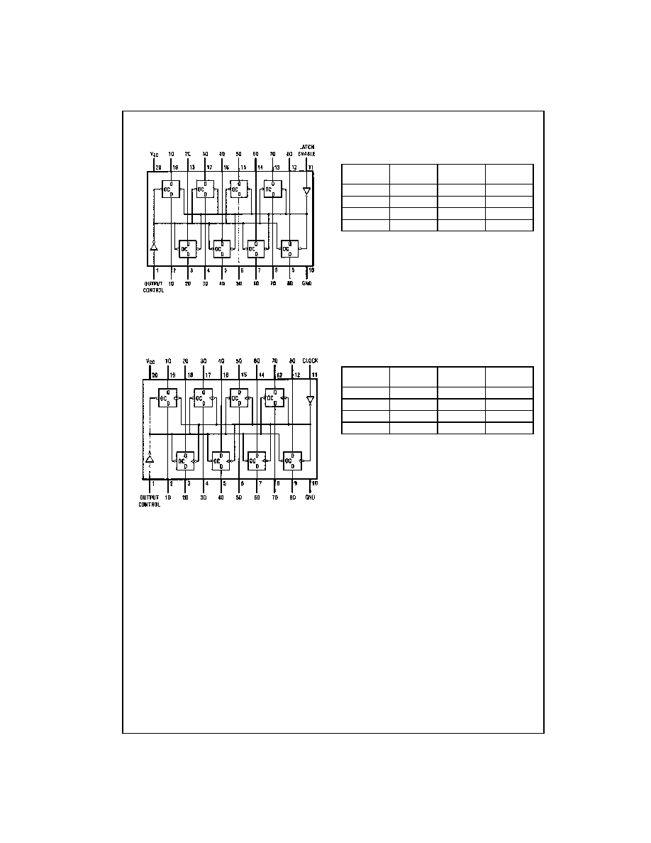
Connection Diagrams
Top View
MM74HCT573
Top View
MM74HCT574
Truth Tables
MM74HCT573
H
=
HIGH Level
L
=
LOW Level
Q
0
=
Level of output before steady-state input conditions were established.
Z
=
High Impedance State
MM74HCT574
H
=
HIGH Level
L
=
LOW Level
Q
0
=
Level of output before steady-state input conditions were established.
X
=
Don't Care
Z
=
High Impedance State
=
Transition from LOW-to-HIGH
Output
Control
LE
Data
Output
L
H
H
H
L
H
L
L
L
L
X
Q
0
H
X
X
Z
Output
Control
LE
Data
Output
L
H
H
L
L
L
L
L
X
Q
0
H
X
X
Z
3
www.fairchildsemi.com
MM74HCT573
· MM74HCT574
Absolute Maximum Ratings
(Note 1)
(Note 2)
Recommended Operating
Conditions
Note 1: Absolute Maximum Ratings are those values beyond which dam-
age to the device may occur.
Note 2: Unless otherwise specified all voltages are referenced to ground.
Note 3: Power Dissipation temperature derating -- plastic "N" package:
-
12 mW/
°
C from 65
°
C to 85
°
C.
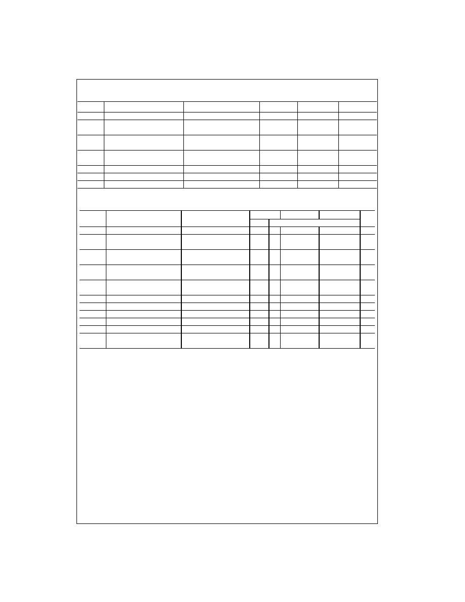
DC Electrical Characteristics
V
CC
=
5V
±
10% (unless otherwise specified)
Note 4: Measured per pin. All others tied to V
CC
or ground.
Supply Voltage (V
CC
)
-
0.5 to
+
7.0V
DC Input Voltage (V
IN
)
-
1.5 to V
CC
+
1.5V
DC Output Voltage (V
OUT
)
-
0.5 to V
CC
+
0.5V
Clamp Diode Current (I
IK
, I
OK
)
±
20 mA
DC Output Current, per pin (I
OUT
)
±
35 mA
DC V
CC
or GND Current, per pin (I
CC
)
±
70 mA
Storage Temperature Range (T
STG
)
-
65
°
C to
+
150
°
C
Power Dissipation (P
D
)
(Note 3)
600 mW
S. O. Package only
500 mW
Lead Temperature (T
L
)
(Soldering 10 seconds)
260
°
C
Min
Max
Units
Supply Voltage (V
CC
)
4.5
5.5
V
DC Input or Output Voltage
(V
IN
, V
OUT
)
0
V
CC
V
Operating Temperature Range (T
A
)
-
40
+
85
°
C
Input Rise or Fall Times
t
r
, t
f
500
ns
Symbol
Parameter
Conditions
T
A
=
25
°
C
T
A
=
-
40 to 85
°
C
T
A
=
-
55 to 125
°
C
Units
Typ
Guaranteed Limits
V
IH
Minimum HIGH Level
2.0
2.0
2.0
V
Input Voltage
V
IL
Maximum LOW Level
0.8
0.8
0.8
V
Input Voltage
V
OH
Minimum HIGH Level
V
IN
=
V
IH
or V
IL
V
Output Voltage
|I
OUT
|
=
20
µ
A
V
CC
V
CC
-
0.1
V
CC
-
0.1
V
CC
-
0.1
|I
OUT
|
=
6.0 mA, V
CC
=
4.5V
4.2
3.98
3.84
3.7
|I
OUT
|
=
7.2 mA, V
CC
=
5.5V
5.7
4.98
4.84
4.7
V
OL
Maximum LOW Level
V
IN
=
V
IH
or V
IL
V
Voltage
|I
OUT
|
=
20
µ
A
0
0.1
0.1
0.1
|I
OUT
|
=
6.0 mA, V
CC
=
4.5V
0.2
0.26
0.33
0.4
|I
OUT
|
=
7.2 mA, V
CC
=
5.5V
0.2
0.26
0.33
0.4
I
IN
Maximum Input
V
IN
=
V
CC
or GND,
±
0.1
±
1.0
±
1.0
µ
A
Current
V
IH
or V
IL
I
OZ
Maximum 3-STATE
V
OUT
=
V
CC
or GND
±
0.5
±
5.0
±
10
µ
A
Output Leakage
Enable
=
V
IH
or V
IL
Current
I
CC
Maximum Quiescent
V
IN
=
V
CC
or GND
8.0
80
160
µ
A
Supply Current
I
OUT
=
0
µ
A
V
IN
=
2.4V or 0.5V (Note 4)
1.5
1.8
2.0
mA
www.fairchildsemi.com
4
MM
74
H
C
T5
73
· MM
74HCT574
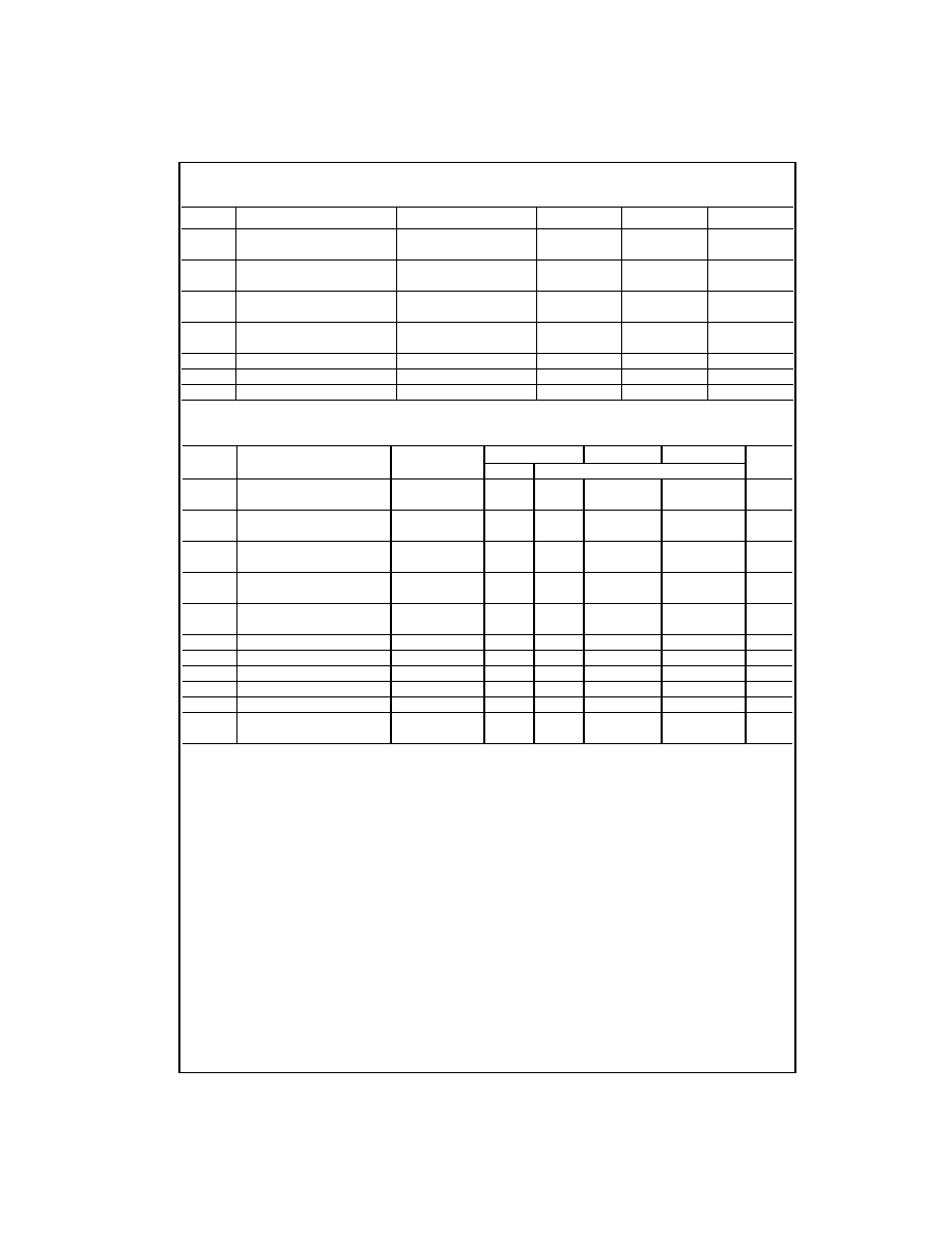
AC Electrical Characteristics
MM74HCT573
V
CC
=
5.0V, t
r
=
t
f
=
6 ns, T
A
=
25
°
C (unless otherwise specified)
AC Electrical Characteristics
MM74HCT573
V
CC
=
5.0V
±
10%, t
r
=
t
f
=
6 ns (unless otherwise specified)
Note 5: C
PD
determines the no load dynamic power consumption, P
D
=
C
PD
V
CC
2 f
+
I
CC
V
CC
, and the no load dynamic current consumption,
I
S
=
C
PD
V
CC
f
+
I
CC
.
Symbol
Parameter
Conditions
Typ
Guaranteed Limit
Units
t
PHL
Maximum Propagation Delay
C
L
=
45 pF
17
27
ns
t
PLH
Data to Output
t
PHL
Maximum Propagation Delay
C
L
=
45 pF
16
27
ns
t
PLH
Latch Enable to Output
t
PZH
Maximum Enable Propagation Delay
C
L
=
45 pF
21
30
ns
t
PZL
Control to Output
R
L
=
1 k
t
PHZ
Maximum Disable Propagation Delay
C
L
=
5 pF
14
23
ns
t
PLZ
Control to Output
R
L
=
1 k
t
W
Minimum Clock Pulse Width
15
ns
t
S
Minimum Setup Time Data to Clock
5
ns
t
H
Minimum Hold Time Clock to Data
12
ns
Symbol
Parameter
Conditions
T
A
=
25
°
T
A
=
-
40 to 85
°
C T
A
=
-
55 to 125
°
C
Units
Typ
Guaranteed Limits
t
PHL
Maximum Propagation
C
L
=
50 pF
18
30
38
45
ns
t
PLH
Delay Data to Output
t
PHL
Maximum Propagation Delay
C
L
=
50 pF
17
30
44
53
ns
t
PLH
Latch Enable to Output
t
PZH
Maximum Enable Propagation
C
L
=
50 pF
22
30
38
45
ns
t
PZL
Delay Control to Output
R
L
=
1 k
t
PHZ
Maximum Disable Propagation
C
L
=
50 pF
15
30
38
45
ns
t
PLZ
Delay Control to Output
R
L
=
1 k
t
THL
Maximum Output
C
L
=
50 pF
6
12
15
18
ns
t
TLH
Rise and Fall Time
t
W
Minimum Clock Pulse Width
15
20
24
ns
t
S
Minimum Setup Time Data to Clock
-
3
5
6
8
ns
t
H
Minimum Hold Time Clock to Data
4
12
15
18
ns
C
IN
Maximum Input Capacitance
10
10
10
pF
C
OUT
Maximum Output Capacitance
20
20
20
pF
C
PD
Power Dissipation Capacitance
OC
=
V
CC
5
pF
(Note 5)
OC
=
GND
52
5
www.fairchildsemi.com
MM74HCT573
· MM74HCT574
AC Electrical Characteristics
MM74HCT574
V
CC
=
5.0V, t
r
=
t
f
=
6 ns, T
A
=
25
°
C
AC Electrical Characteristics
MM74HCT574
V
CC
=
5.0V
±
10%, t
r
=
t
f
=
6 ns (unless otherwise specified)
Note 6: C
PD
determines the no load power consumption, P
D
=
C
PD
V
CC
2
f
+
I
CC
V
CC
, and the no load dynamic current consumption, I
S
=
C
PD
V
CC
f
+
I
CC
.
Symbol
Parameter
Conditions
Typ
Guaranteed Limit
Units
f
MAX
Maximum Clock Frequency
60
33
MHz
t
PHL
Maximum Propagation Delay
C
L
=
45 pF
17
27
ns
t
PLH
to Output
t
PZH
Maximum Enable Propagation Delay
C
L
=
45 pF
19
28
ns
t
PZL
Control to Output
R
L
=
1 k
t
PHZ
Maximum Disable Propagation Delay
C
L
=
45 pF
14
25
ns
t
PLZ
Control to Output
R
L
=
1 k
t
W
Minimum Clock Pulse Width
15
ns
t
S
Minimum Setup Time Data to Clock
12
ns
t
H
Minimum Hold Time Clock to Data
5
ns
Symbol
Parameter
Conditions
T
A
=
25
°
C
T
A
=
-
40 to 85
°
C T
A
=
-
55 to 125
°
C
Units
Typ
Guaranteed Limits
f
MAX
Maximum Clock Frequency
33
28
23
MHz
t
PHL
Maximum Propagation Delay
C
L
=
50 pF
18
30
38
45
ns
t
PLH
Clock to Output
t
PZH
Maximum Enable Propagation
C
L
=
50 pF
22
30
38
45
ns
t
PZL
Delay Control to Output
R
L
=
1 k
t
PHZ
Maximum Disable Propagation
C
L
=
50 pF
15
30
38
45
ns
t
PLZ
Delay Control to Output
R
L
=
1 k
t
THL
Maximum Output
C
L
=
50 pF
6
12
15
18
ns
t
TLH
Rise and Fall Time
t
W
Minimum Clock Pulse Width
15
20
24
ns
t
S
Minimum Setup Time Data to Clock
6
12
15
18
ns
t
H
Minimum Hold Time Clock to Data
-
1
5
6
8
ns
C
IN
Maximum Input Capacitance
10
10
10
pF
C
OUT
Maximum Output Capacitance
20
20
20
pF
C
PD
Power Dissipation Capacitance
OC
=
V
CC
5
pF
(Note 6)
OC
=
GND
58