 | ÐлекÑÑоннÑй компоненÑ: MOC211 | СкаÑаÑÑ:  PDF PDF  ZIP ZIP |
Äîêóìåíòàöèÿ è îïèñàíèÿ www.docs.chipfind.ru
4/10/03
SMALL OUTLINE OPTOCOUPLERS
TRANSISTOR OUTPUT
Page 1 of 9
© 2002 Fairchild Semiconductor Corporation
MOC211-M
MOC212-M
MOC213-M
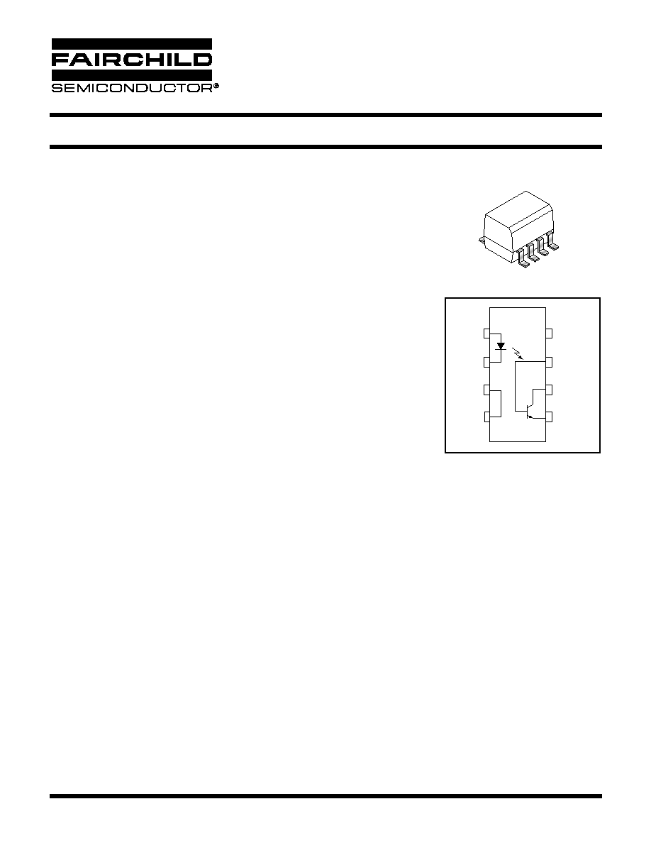
DESCRIPTION
These devices consist of a gallium arsenide infrared emitting diode optically coupled to a
monolithic silicon phototransistor detector, in a surface mountable, small outline, plastic
package. They are ideally suited for high density applications, and eliminate the need for
through-the-board mounting.
FEATURES
· UL Recognized (File #E90700, volume 2)
· VDE Recognized (File #136616) (add option `V' for VDE approval, e.g., MOC211V-M)
· Convenient Plastic SOIC-8 Surface Mountable Package Style
· Standard SOIC-8 Footprint, with 0.050" Lead Spacing
· Compatible with Dual Wave, Vapor Phase and IR Reflow Soldering
· High Input-Output Isolation of 2500 V
AC(rms)
Guaranteed
· Minimum BV
CEO
of 30V guaranteed
APPLICATIONS
· General Purpose Switching Circuits
· Interfacing and coupling systems of different potentials and impedances
· Regulation Feedback Circuits
· Monitor and Detection Circuits
BASE
N/C
ANODE
CATHODE
1
2
3
4
5
6
7
8
EMITTER
COLLECTOR
N/C
N/C

4/10/03
Page 2 of 9
© 2002 Fairchild Semiconductor Corporation
SMALL OUTLINE OPTOCOUPLERS
TRANSISTOR OUTPUT
MOC211-M
MOC212-M
MOC213-M
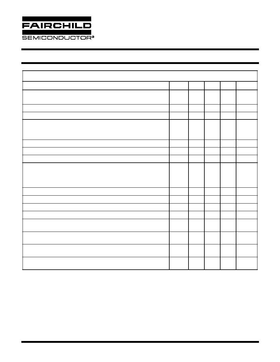
ABSOLUTE MAXIMUM RATINGS
(T
A
= 25°C Unless otherwise specified)
Rating
Symbol
Value
Unit
EMITTER
Forward Current Continuous
I
F
60
mA
Forward Current Peak (PW = 100 µs, 120 pps)
I
F
(pk)
1.0
A
Reverse Voltage
V
R
6.0
V
LED Power Dissipation @ T
A
= 25°C
Derate above 25°C
P
D
90
0.8
mW
mW/°C
DETECTOR
Collector-Emitter Voltage
V
CEO
30
V
Emitter-Collector Voltage
V
ECO
7.0
V
Collector-Base Voltage
V
CBO
70
V
Collector Current-Continuous
I
C
150
mA
Detector Power Dissipation @ T
A
= 25°C
Derate above 25°C
P
D
150
1.76
mW
mW/°C
TOTAL DEVICE
Input-Output Isolation Voltage (1,2,3)
(f = 60 Hz, t = 1 min.)
V
ISO
2500
Vac(rms)
Total Device Power Dissipation @ T
A
= 25°C
Derate above 25°C
P
D
250
2.94
mW
mW/°C
Ambient Operating Temperature Range
T
A
-40 to +100
°C
Storage Temperature Range
T
stg
-40 to +150
°C
4/10/03
Page 3 of 9
© 2002 Fairchild Semiconductor Corporation
SMALL OUTLINE OPTOCOUPLERS
TRANSISTOR OUTPUT
MOC211-M
MOC212-M
MOC213-M
** Typical values at T
A
= 25°C
1. Isolation Surge Voltage, V
ISO
, is an internal device dielectric breakdown rating.
2. For this test, Pins 1 and 2 are common and Pins 5, 6 and 7 are common.
3. V
ISO
rating of 2500 V
AC(rms)
for t = 1 min. is equivalent to a rating of 3,000 V
AC(rms)
for t = 1 sec.
4. Current Transfer Ratio (CTR) = I
C
/I
F
x 100%.
ELECTRICAL CHARACTERISTICS
(T
A
= 25°C Unless otherwise specified)
Parameter
Test Conditions
Symbol
Min
Typ**
Max
Unit
EMITTER
Input Forward Voltage
(I
F
= 10 mA)
V
F
--
1.15
1.5
V
Reverse Leakage Current
(V
R
= 6.0 V)
I
R
--
0.001
100
µA
Input Capacitance
C
IN
--
18
--
pF
DETECTOR
Collector-Emitter Dark Current
(V
CE
= 10 V, T
A
= 25°C)
(V
CE
= 10 V, T
A
= 100°C)
I
CEO1
I
CEO2
--
--
1.0
1.0
50
--
nA
µA
Collector-Emitter Breakdown Voltage
(I
C
= 100 µA)
BV
CEO
30
90
--
V
Emitter-Collector Breakdown Voltage
(I
E
= 100 µA)
BV
ECO
7.0
7.8
--
V
Collector-Emitter Capacitance
(f = 1.0 MHz, V
CE
= 0)
C
CE
--
7.0
--
pF
COUPLED
Collector-Output Current
(4)
MOC211-M
MOC212-M
(I
F
= 10 mA, V
CE
= 10 V)
MOC213-M
CTR
20
50
100
65
90
140
--
--
--
%
Isolation Surge Voltage
(1,2,3)
(60 Hz AC Peak, 1 min.)
V
ISO
2500
--
--
Vac(rms)
Isolation Resistance
(2)
(V = 500 V)
R
ISO
10
11
--
--
Collector-Emitter Saturation Voltage
(I
C
= 2.0 mA, I
F
= 10 mA)
V
CE (sat)
--
0.15
0.4
V
Isolation Capacitance
(2)
(V = 0 V, f = 1 MHz)
C
ISO
--
0.2
--
pF
Turn-On Time
(I
C
= 2.0 mA, V
CC
= 10 V, R
L
= 100
)
(Fig. 6)
t
on
--
7.5
--
µs
Turn-Off Time
(I
C
= 2.0 mA, V
CC
= 10 V, R
L
= 100
)
(Fig. 6)
t
off
--
5.7
--
µs
Rise Time
(I
C
= 2.0 mA, V
CC
= 10 V, R
L
= 100
)
(Fig. 6)
t
r
--
3.2
--
µs
Fall Time
(I
C
= 2.0 mA, V
CC
= 10 V, R
L
= 100
)
(Fig. 6)
t
f
--
4.7
--
µs
4/10/03
Page 4 of 9
© 2002 Fairchild Semiconductor Corporation
SMALL OUTLINE OPTOCOUPLERS
TRANSISTOR OUTPUT
MOC211-M
MOC212-M
MOC213-M
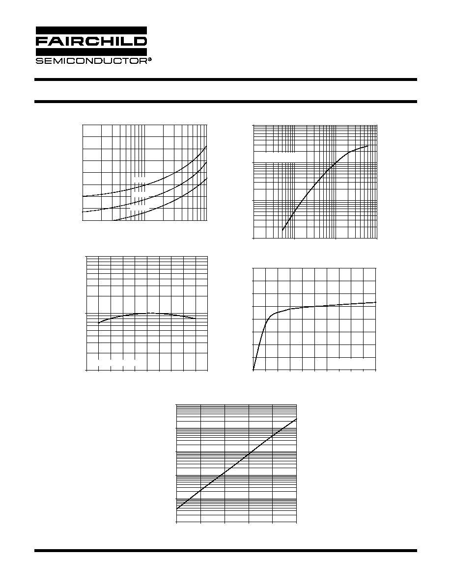
Fig. 2 Output Curent vs. Input Current
I
F
- LED INPUT CURRENT (mA)
0.1
1
10
100
I
C
- OU
T
P
U
T
C
O
L
L
EC
T
O
R
CU
R
R
E
N
T
(
N
O
R
MA
L
I
Z
E
D
)
0.01
0.1
1
10
V
CE
= 5V
NORMALIZED TO I
F
= 10mA
Fig. 3 Output Current vs. Ambient Temperature
T
A
- AMBIENT TEMPERATURE (
°C)
-80
-60
-40
-20
0
20
40
60
80
100
120
I
C
- OU
T
P
U
T
C
O
L
L
EC
T
O
R
CU
R
R
E
N
T (
N
O
R
M
A
L
I
ZE
D
)
0.1
1
10
NORMALIZED TO T
A
= 25
°C
Fig. 4 Output Current vs. Collector - Emitter Voltage
V
CE
- COLLECTOR -EMITTER VOLTAGE (V)
0
1
2
3
4
5
6
7
8
9
10
I
C
- O
U
T
P
U
T
CO
L
L
EC
T
O
R
CU
R
R
E
N
T
(
N
OR
M
A
L
I
Z
E
D
)
0.0
0.2
0.4
0.6
0.8
1.0
1.2
1.4
1.6
I
F
= 10mA
NORMALIZED TO V
CE
= 5V
Fig. 5 Dark Current vs. Ambient Temperature
T
A
- AMBIENT TEMPERATURE (
°C)
0
20
40
60
80
100
I
CE
O
- C
O
L
L
E
C
T
O
R -
E
M
I
T
T
E
R
D
A
RK
CU
RR
E
N
T
(
n
A
)
0.1
1
10
100
1000
10000
V
CE
=10V
I
F
- LED FORWARD CURRENT (mA)
V
F
- FOR
W
ARD
V
O
L
T
A
GE (V)
Fig. 1 LED Forward Voltage vs. Forward Current
1
10
100
1.0
1.1
1.2
1.3
1.4
1.5
1.6
1.7
1.8
T
A
= 55
°C
T
A
= 25
°C
T
A
= 100
°C
4/10/03
Page 5 of 9
© 2002 Fairchild Semiconductor Corporation
SMALL OUTLINE OPTOCOUPLERS
TRANSISTOR OUTPUT
MOC211-M
MOC212-M
MOC213-M
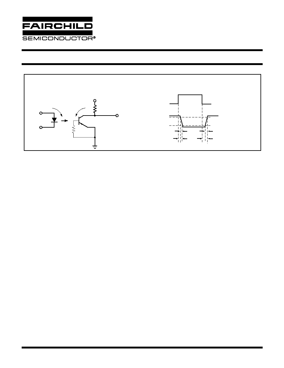
OUTPUT PULSE
INPUT PULSE
TEST CIRCUIT
WAVE FORMS
t
r
t
f
INPUT
I
F
R
L
R
BE
V
CC
= 10V
OUTPUT
t
on
10%
90%
t
off
Figure 6. Switching Time Test Circuit and Waveforms
I
C
Adjust I
F
to produce I
C
= 2 mA