 | ÐлекÑÑоннÑй компоненÑ: NDS9933 | СкаÑаÑÑ:  PDF PDF  ZIP ZIP |
Äîêóìåíòàöèÿ è îïèñàíèÿ www.docs.chipfind.ru
NDS9933A
NDS9933A Rev. A
NDS9933A
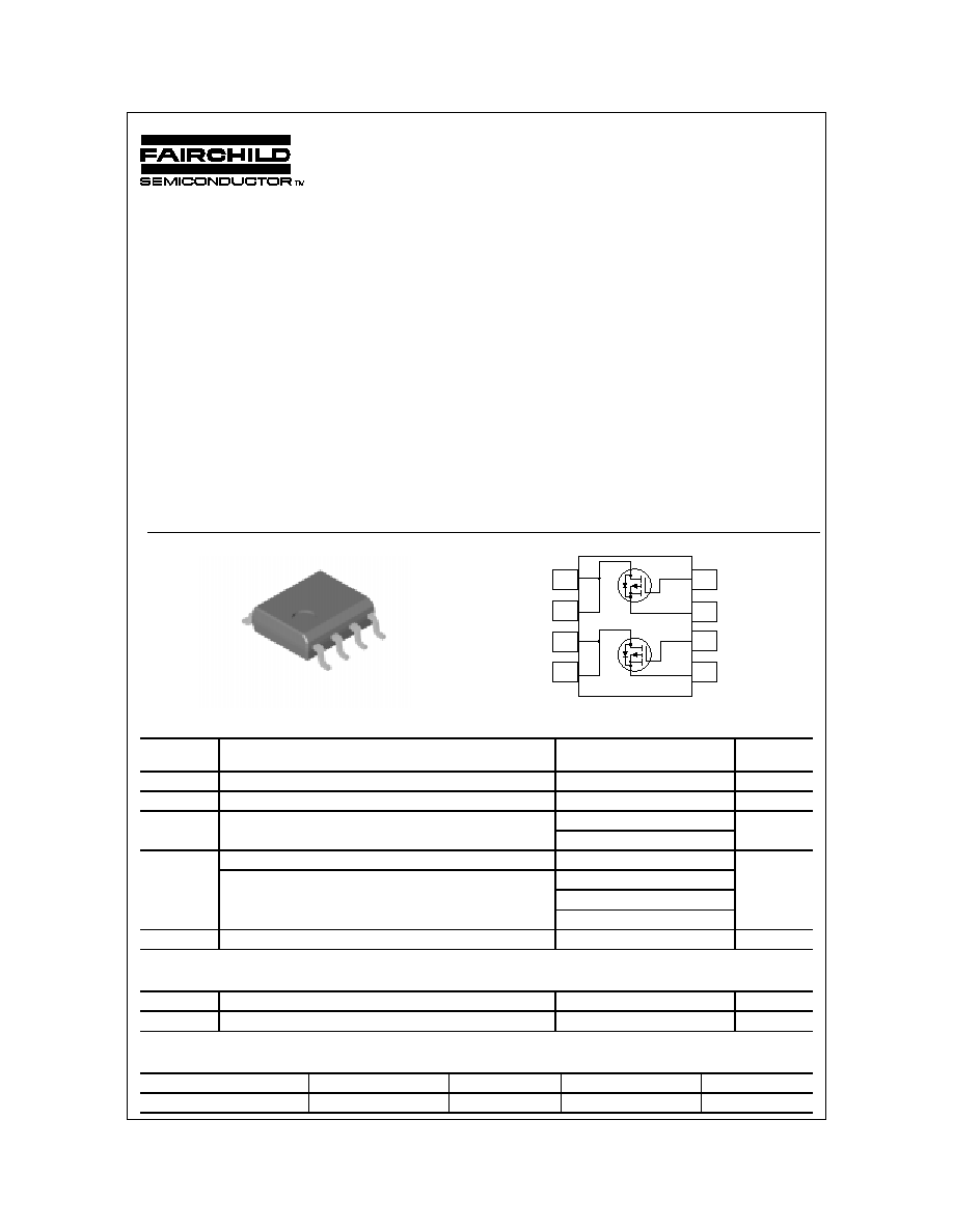
Dual P-Channel Enhancement Mode Field Effect Transistor
General Description
This P-Channel enhancement mode power field ef-
fect transistor is produced using Fairchild's propri-
etary, high cell density, DMOS technology. This very
high density process is especially tailored to mini-
mize on-state resistance and provide superior
switching performance.
These devices are particularly suited for low voltage
apllications such as DC motor control and DC/
DC conversion where fast switching,low in-line
power loss, and resistance to transients are
needed.
January 1999
Features
·
-2.8 A, -20 V. R
DS(on)
= 0.14
@ V
GS
= -4.5 V
R
DS(on)
= 0.19
@ V
GS
= -2.7 V
R
DS(on)
= 0.20
@ V
GS
= -2.5 V.
·
High density cell design for extremely low R
DS(on)
.
·
High power and current handling capability in a
widely used surface mount package.
©
1999 Fairchild Semiconductor Corporation
Absolute Maximum Ratings
T
A
= 25°C unless otherwise noted
Symbol
Parameter
NDS9933A
Units
V
DSS
Drain-Source Voltage
-20
V
V
GSS
Gate-Source Voltage
±
8
V
I
D
Drain Current
- Continuous
(Note 1a)
-2.8
A
- Pulsed
-10
Power Dissipation for Dual Operation
2
Power Dissipation for Single Operation
(Note 1a)
1.6
(Note 1b)
1
P
D
(Note 1c)
0.9
W
T
J
, T
stg
Operating and Storage Junction Temperature Range
-55 to +150
°
C
Thermal Characteristics
R
JA
Thermal Resistance, Junction-to-Ambient
(Note 1a)
78
°
C/W
R
JC
Thermal Resistance, Junction-to-Case
(Note 1)
40
°
C/W
Package Outlines and Ordering Information
Device Marking
Device
Reel Size
Tape Width
Quantity
NDS9933A
NDS9933A
13''
12mm
2500 units
·
Dual MOSFET in surface mount package.
1
5
7
8
2
3
4
6
SO-8
D1
D1
D2
D2
S1
G1
S2
G1
NDS9933A
NDS9933A Rev. A
Electrical Characteristics
T
A
= 25°C unless otherwise noted
Symbol
Parameter
Test Conditions
Min Typ Max Units
Off Characteristics
BV
DSS
Drain-Source Breakdown Voltage
V
GS
= 0 V, I
D
= -250
µ
A
-20
V
BV
DSS
T
J
Breakdown Voltage Temperature
Coefficient
I
D
= -250
µ
A, Referenced to 25
°
C
-25
mV/
°
C
I
DSS
Zero Gate Voltage Drain Current
V
DS
= -16 V, V
GS
= 0 V
-1
µ
A
I
GSSF
Gate-Body Leakage Current, Forward
V
GS
= 8 V, V
DS
= 0 V
100
nA
I
GSSR
Gate-Body Leakage Current, Reverse
V
GS
= -8 V, V
DS
= 0 V
-100
nA
On Characteristics
(Note 2)
V
GS(th)
Gate Threshold Voltage
V
DS
= V
GS
, I
D
= -250
µ
A
-0.4
-0.65
-1
V
V
GS(th)
T
J
Gate Threshold Voltage
Temperature Coefficient
I
D
= -250
µ
A, Referenced to 25
°
C
4
mV/
°
C
R
DS(on)
Static Drain-Source
On-Resistance
V
GS
= -4.5 V, I
D
= -2.8 A
V
GS
= -4.5 V, I
D
= -2.8A,T
J
=125
°
C
V
GS
= -2.7 V, I
D
= -1.5 A
V
GS
= -2.5 V, I
D
= -1.5 A
0.10
5
0.15
0
0.13
5
0.14
0
0.140
0.240
0.190
0.200
I
D(on)
On-State Drain Current
V
GS
= -4.5 V, V
DS
= -5 V
-10
A
g
FS
Forward Transconductance
V
DS
= -5 V, I
D
= -2.8 A
6.5
S
Dynamic Characteristics
C
iss
Input Capacitance
405
pF
C
oss
Output Capacitance
170
pF
C
rss
Reverse Transfer Capacitance
V
DS
= -10 V, V
GS
= 0 V,
f = 1.0 MHz
45
pF
Switching Characteristics
(Note 2)
t
d(on)
Turn-On Delay Time
6.5
13
ns
t
r
Turn-On Rise Time
20
35
ns
t
d(off)
Turn-Off Delay Time
31
50
ns
t
f
Turn-Off Fall Time
V
DD
= -5 V, I
D
= -1 A,
V
GS
= -4.5 V, R
GEN
= 6
21
35
ns
Q
g
Total Gate Charge
6
8.5
nC
Q
gs
Gate-Source Charge
0.8
nC
Q
gd
Gate-Drain Charge
V
DS
= -5 V, I
D
= -2.8 A,
V
GS
= -4.5 V,
1.3
nC
Drain-Source Diode Characteristics and Maximum Ratings
I
S
Maximum Continuous Drain-Source Diode Forward Current
-1.3
A
V
SD
Drain-Source Diode Forward Voltage
V
GS
= 0 V, I
S
= -1.3 A
(Note 2)
-0.78
-1.2
V
Notes:
1: R
JA
is the sum of the junction-to-case and case-to-ambient resistance where the case thermal reference is defined as the solder mounting surface of
the drain pins. R
JC
is guaranteed by design while R
JA
is determined by the user's board design.
Scale 1 : 1 on letter size paper
2: Pulse Test: Pulse Width
300
µ
s, Duty Cycle
2.0%
c. 135
O
C/W on a 0.003 in
2
pad of 2oz copper.
b. 125
O
C/W on a 0.02 in
2
pad of 2oz copper.
a. 78
O
C/W on a 0.5 in
2
pad of 2oz copper.
NDS9933A
NDS9933A Rev. A
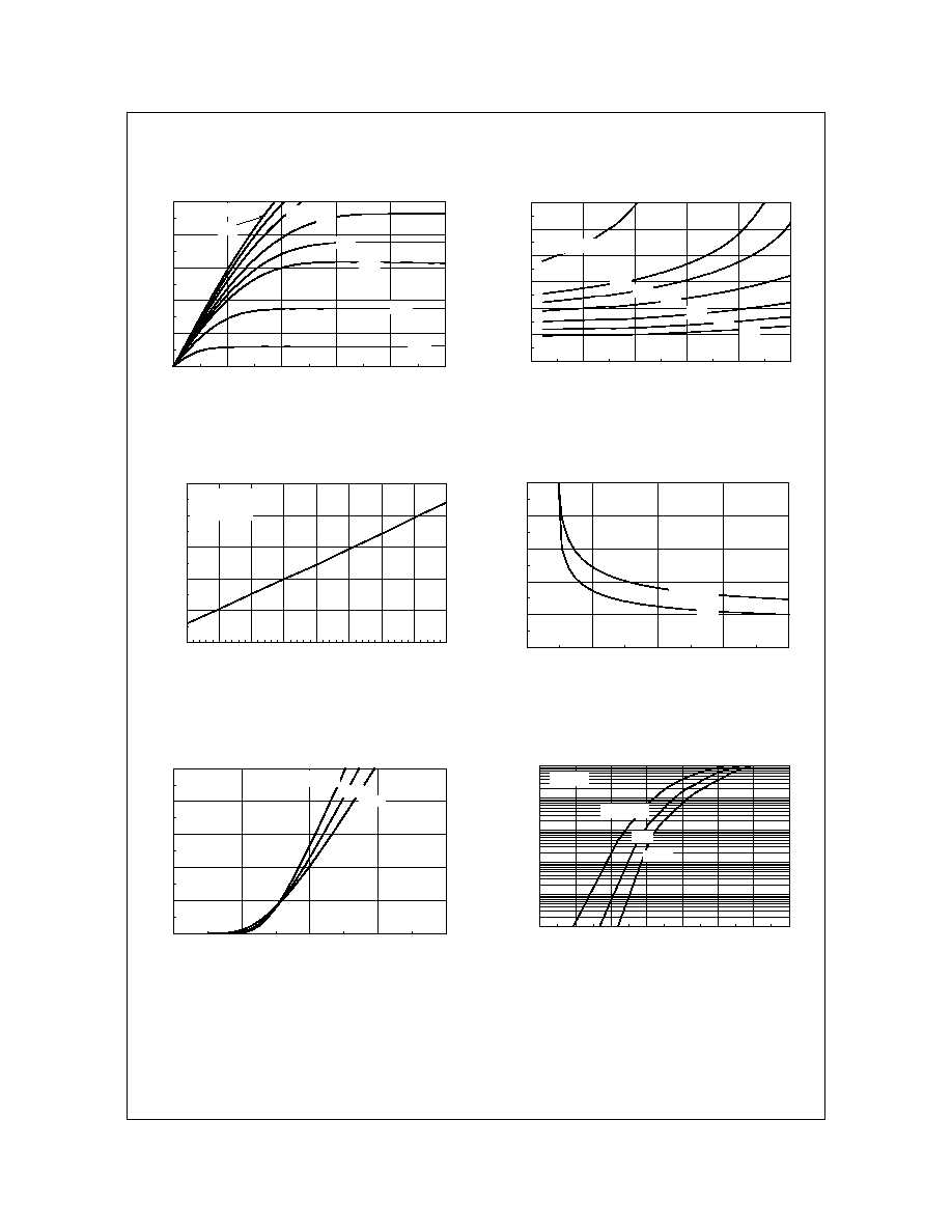
Typical Characteristics
Figure 1. On-Region Characteristics.
Figure 2. On-Resistance Variation
with Drain Current and Gate Voltage.
Figure 3. On-Resistance Variation
with Temperature.
Figure 4. On-Resistance Variation
with Gate-to-Source Voltage.
Figure 5. Transfer Characteristics.
Figure 6. Body Diode Forward Voltage
Variation with Source Current
and Temperature.
0
2
4
6
8
10
0.8
1
1.2
1.4
1.6
1.8
2
-I , DRAIN CURRENT (A)
DRA
IN-
S
O
URCE
O
N
-
R
E
S
I
S
T
A
NCE
V = -2.0V
GS
D
R
, N
O
R
M
ALIZ
ED
DS(O
N)
-3.0
-3.5
-4.5
-4.0
-2.5
-2.7
0
1
2
3
4
5
0
3
6
9
12
15
-V , DRAIN-SOURCE VOLTAGE (V)
-I
,
D
R
A
I
N
-
S
O
UR
CE
CU
RRE
NT (A
)
V = -4.5V
GS
-2.5
DS
D
-4.0
-3.0
-3.5
-2.0
-1.5
-2.7
R
, N
O
R
M
ALIZ
ED
DS(
O
N)
-50
-25
0
25
50
75
100
125
150
0.6
0.8
1
1.2
1.4
1.6
T , JUNCTION TEMPERATURE (°C)
DR
A
I
N-
S
O
URCE
O
N
-
R
E
S
I
S
TA
NCE
J
V = -4.5V
GS
I = -2.8A
D
1
2
3
4
5
0
0.1
0.2
0.3
0.4
0.5
-V ,GATE TO SOURCE VOLTAGE (V)
R
,O
N
-
R
E
S
I
S
T
A
N
C
E
(
O
H
M
)
GS
25°C
T = 125°C
J
I = -1.4A
D
DS(O
N)
0
1
2
3
4
0
2
4
6
8
10
-V , GATE TO SOURCE VOLTAGE (V)
-
I
,
D
R
A
I
N
CUR
RE
NT (
A
)
V = -5V
DS
GS
D
T = -55°C
A
125°C
25°C
0
0.2
0.4
0.6
0.8
1
1.2
1.4
0.0001
0.001
0.01
0.1
1
10
-V , BODY DIODE FORWARD VOLTAGE (V)
-I
,
R
EVER
SE
D
R
AI
N
C
U
R
R
EN
T
(A)
25°C
-55°C
V = 0V
GS
SD
S
T = 125°C
J
NDS9933A
NDS9933A Rev. A
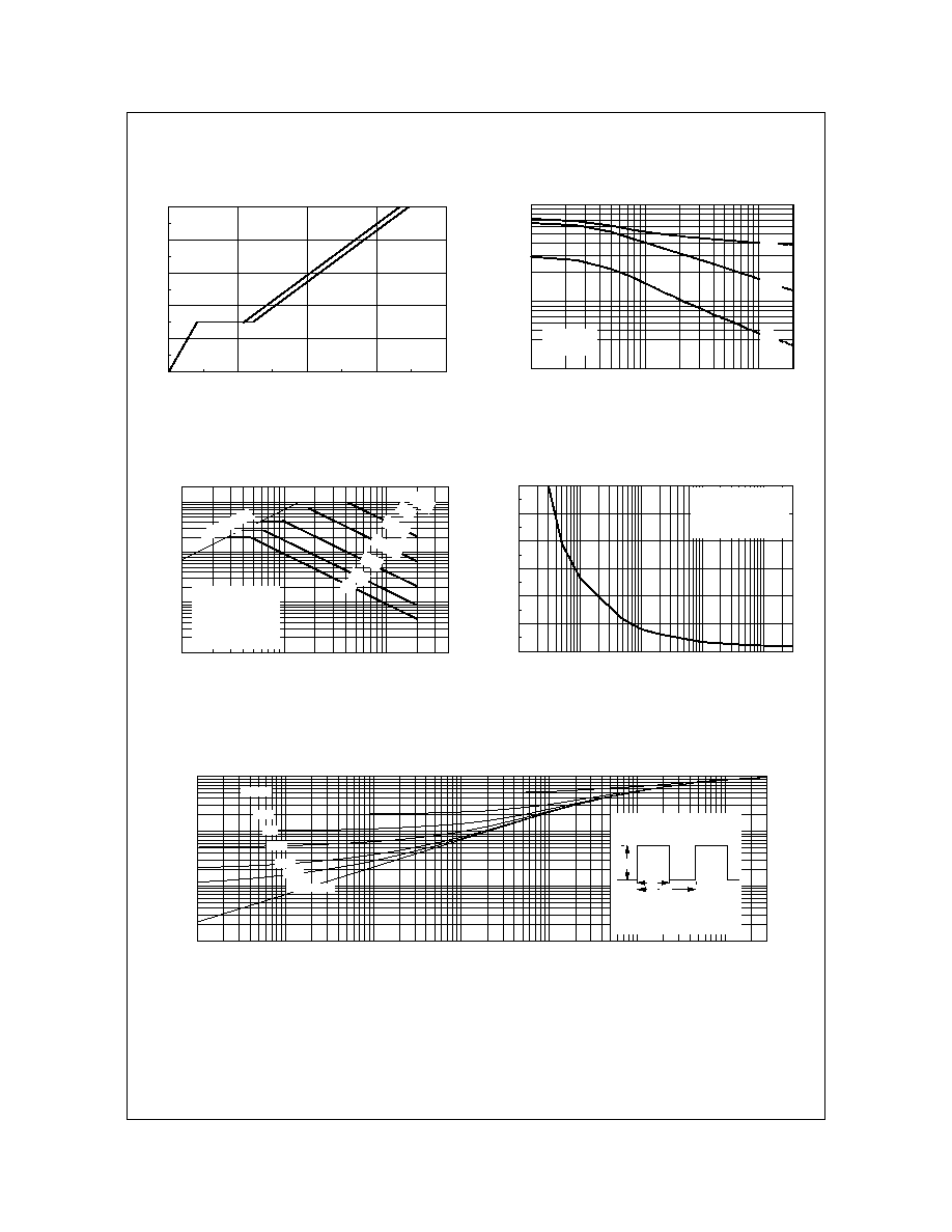
Typical Characteristics
(continued)
Figure 7. Gate-Charge Characteristics.
Figure 8. Capacitance Characteristics.
Figure 9. Maximum Safe Operating Area.
Figure 10. Single Pulse Maximum
Power Dissipation.
Figure 11. Transient Thermal Response Curve.
Thermal characterization performed using the conditions described in Note 1.
Transient themal response will change depending on the circuit board design.
0.0001
0.001
0.01
0.1
1
10
100
300
0.001
0.002
0.005
0.01
0.02
0.05
0.1
0.2
0.5
1
t , TIME (sec)
T
R
A
N
S
I
E
NT
T
H
E
RM
AL RE
S
I
S
T
AN
CE
r
(
t
)
,
NO
RM
AL
I
Z
E
D
E
F
F
E
CT
I
V
E
1
Single Pulse
D = 0.5
0.1
0.05
0.02
0.01
0.2
Duty Cycle, D = t /t
1
2
R (t) = r(t) * R
R = 135°C/W
JA
JA
JA
T - T = P * R (t)
JA
A
J
P(pk)
t
1
t
2
0
2
4
6
8
0
1
2
3
4
5
Q , GATE CHARGE (nC)
-
V
, G
A
T
E
-
S
O
U
R
C
E
V
O
L
T
A
G
E
(
V
)
g
GS
V = -5V
DS
I = -2.8A
D
-15V
0.1
0.2
0.5
1
2
5
10
20
20
50
100
200
400
600
1000
-V , DRAIN TO SOURCE VOLTAGE (V)
CA
P
A
C
I
T
A
NCE
(
p
F)
DS
C
iss
f = 1 MHz
V = 0 V
GS
C
oss
C
rss
0.1
0.2
0.5
1
2
5
10
20
40
0.01
0.05
0.1
0.5
1
2
5
10
20
- V , DRAIN-SOURCE VOLTAGE (V)
-
I
, D
R
A
I
N C
URR
E
N
T (
A
)
RDS
(O
N)
LI
MI
T
D
A
DC
DS
1s
100m
s
10m
s
1m
s
10s
V = -4.5V
SINGLE PULSE
R =135°C/W
T = 25°C
JA
GS
A
10
0
µ
s
0.01
0.1
0.5
10
50 100
300
0
5
10
15
20
25
30
SINGLE PULSE TIME (SEC)
POWER
(
W
)
SINGLE PULSE
R =135 °C/W
T = 25°C
JA
A
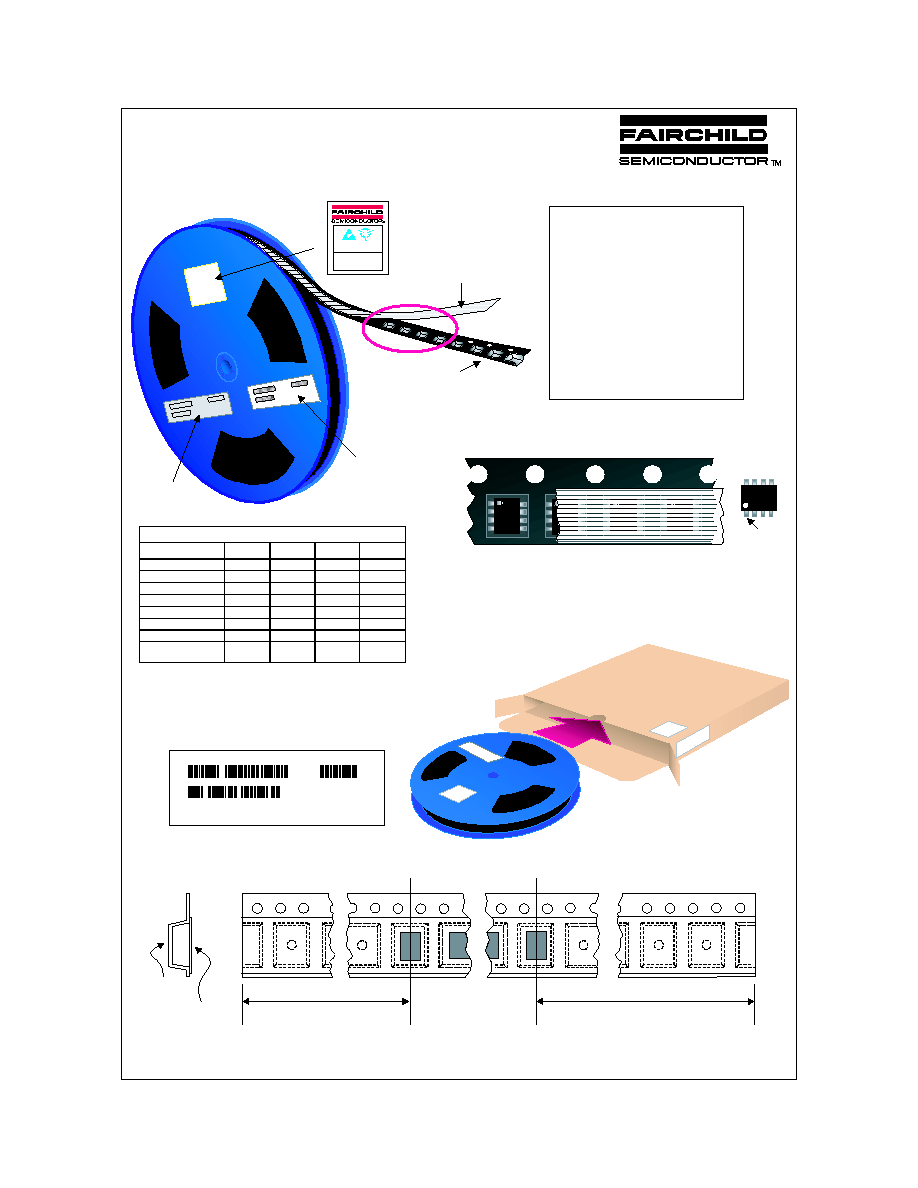
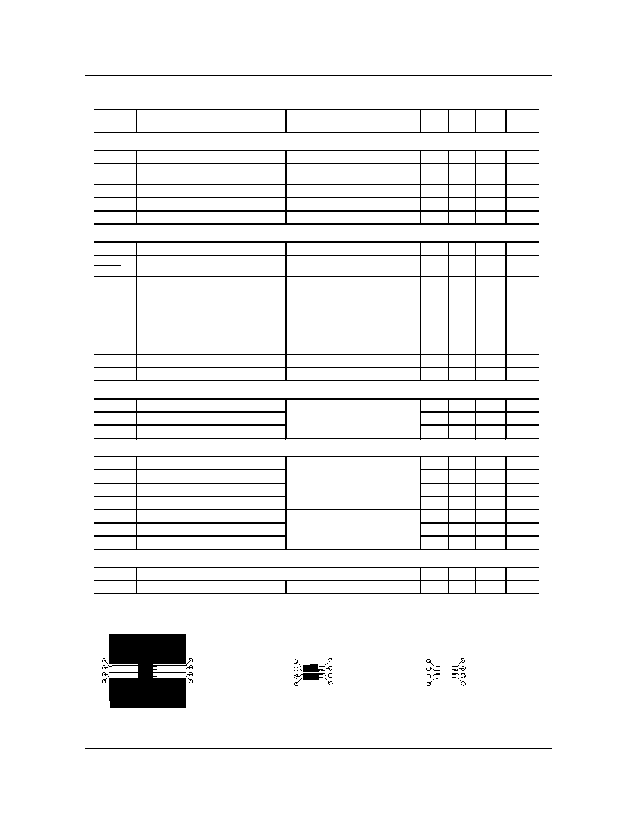
SOIC(8lds) Packaging
Configuration: Figure 1.0
Components
Leader Tape
1680mm minimum or
210 empty pockets
Trailer Tape
640mm minimum or
80 empty pockets
SOIC(8lds) Tape Leader and Trailer
Configuration: Figure 2.0
Cover Tape
Carrier Tape
Note/Comments
Packaging Option
SOIC (8lds) Packaging Information
Standard
(no flow code)
L86Z
F011
Packaging type
Reel Size
TNR
13" Dia
Rail/Tube
-
TNR
13" Dia
Qty per Reel/Tube/Bag
2,500
95
4,000
Box Dimension (mm)
343x64x343
530x130x83
343x64x343
Max qty per Box
5,000
30,000
8,000
D84Z
TNR
7" Dia
500
184x187x47
1,000
Weight per unit (gm)
0.0774
0.0774
0.0774
0.0774
Weight per Reel (kg)
0.6060
-
0.9696
0.1182
F63TN Label
ESD Label
343mm x 342mm x 64mm
Standard Intermediate box
ESD Label
F63TNR Label sample
F63TNLabel
LOT: CBVK741B019
FSID: FDS9953A
D/C1: D9842 QTY1:
SPEC REV:
SPEC:
QTY: 2500
D/C2:
QTY2:
CPN:
N/F: F (F63TNR)3
F852
NDS
9959
SOIC-8 Unit Orientation
F
85
2
NDS
99
59
Pin 1
Static Dissipative
Embossed Carrier Tape
F63TNR
Label
Antistatic Cover Tape
ESD Label
EL ECT RO ST AT IC
SEN SIT IVE DEVI CES
DO NO T SHI P OR STO RE N EAR ST RO NG EL ECT ROST AT IC
EL ECT RO M AGN ETI C, M AG NET IC O R R ADIO ACT IVE FI ELD S
TNR D ATE
PT NUMB ER
PEEL STREN GTH MIN ___ __ ____ __ ___gms
MAX ___ ___ ___ ___ _ gms
Customized
Label
Packaging Description:
SOIC-8 parts are shipped in tape. The carrier tape is
made from a dissipative (carbon filled) polycarbonate
resin. The cover tape is a multilayer film (Heat Activated
Adhesive in nature) primarily composed of polyester film,
adhesive layer, sealant, and anti-static sprayed agent.
These reeled parts in standard option are shipped with
2,500 units per 13" or 330cm diameter reel. The reels are
dark blue in color and is made of polystyrene plastic (anti-
static coated). Other option comes in 500 units per 7" or
177cm diameter reel. This and some other options are
further described in the Packaging Information table.
These full reels are individually barcode labeled and
placed inside a standard intermediate box (illustrated in
figure 1.0) made of recyclable corrugated brown paper.
One box contains two reels maximum. And these boxes
are placed inside a barcode labeled shipping box which
comes in different sizes depending on the number of parts
shipped.
F
85
2
NDS
99
59
F
85
2
NDS
99
59
F
85
2
NDS
99
59
SO-8 Tape and Reel Data and Package Dimensions
July 1999, Rev. B