 | –≠–ª–µ–∫—Ç—Ä–æ–Ω–Ω—ã–π –∫–æ–º–ø–æ–Ω–µ–Ω—Ç: RC1584 | –°–∫–∞—á–∞—Ç—å:  PDF PDF  ZIP ZIP |
www.fairchildsemi.com
REV. 1.0.5 7/13/00
Features
∑ Fast transient response
∑ Low dropout voltage at up to 7A
∑ Load regulation: 0.05% typical
∑ Trimmed current limit
∑ On-chip thermal limiting
∑ Standard TO-220, TO-263 and TO-263 center cut
packages
Applications
∑ Pentium
Æ
Class GTL+ bus supply
∑ Low voltage logic supply
∑ Post regulator for switching supply
Description
The RC1584 and RC1584-1.5 are low dropout three-terminal
regulators with 7A output current capability. These devices
have been optimized for low voltage applications including
V
TT
bus termination, where transient response and minimum
input voltage are critical. The RC1584 is ideal for low
voltage microprocessor applications requiring a regulated
output from 1.5V to 3.6V with an input supply of 5V or less.
The RC1584-1.5 offers fixed 1.5V with 7A current capabil-
ity for GTL+ bus V
TT
termination.
Current limit is trimmed to ensure specified output current
and controlled short-circuit current. On-chip thermal limiting
provides protection against any combination of overload and
ambient temperature that would create excessive junction
temperatures.
The RC1584 and RC1584-1.5 are available in the industry-
standard TO-220, TO-263 and TO-263 center cut power
packages.
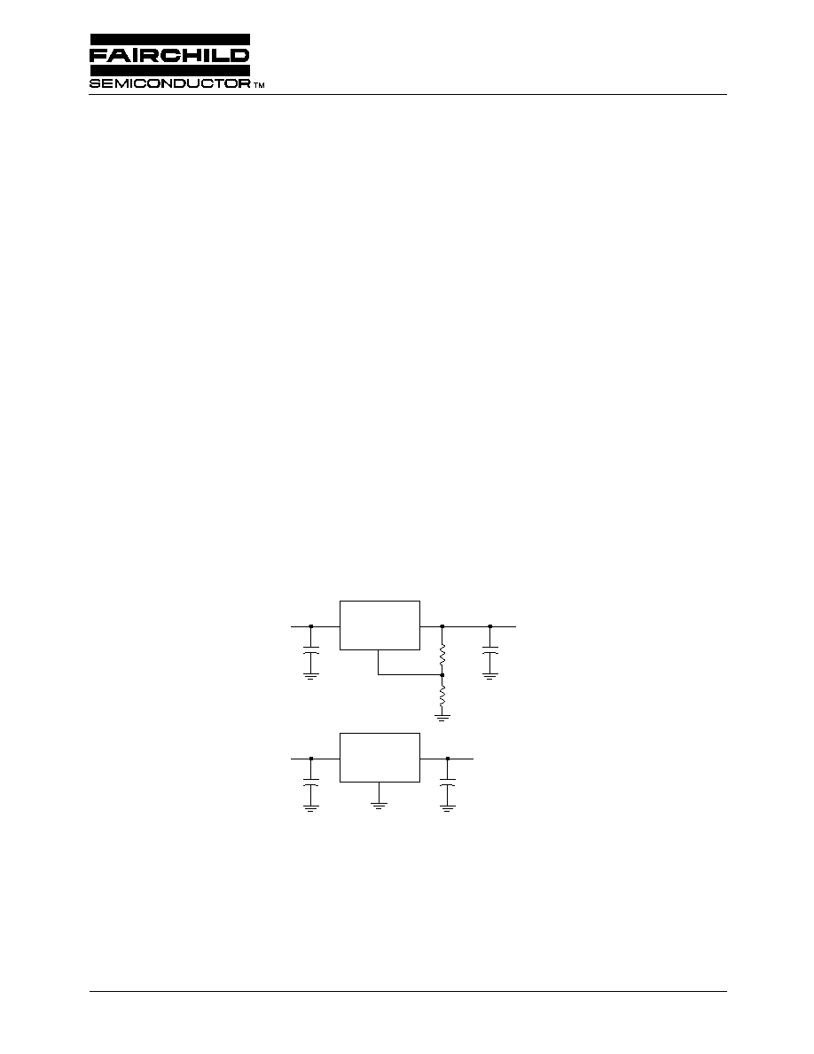
Typical Applications
V
IN = 3.3V
10
µ
F
10
µ
F
22
µ
F
124
24.9
22
µ
F
1.5V at 7A
+
+
V
IN
ADJ
V
OUT
RC1584
V
IN = 3.3V
1.5V at 7A
+
+
V
IN
GND
V
OUT
RC1584-1.5
65-1584-16
RC1584
7A Adjustable/Fixed Low Dropout Linear Regulator
Pentium is a registered trademark of Intel Corporation.
RC1584
PRODUCT SPECIFICATION
2
REV. 1.0.5 7/13/00
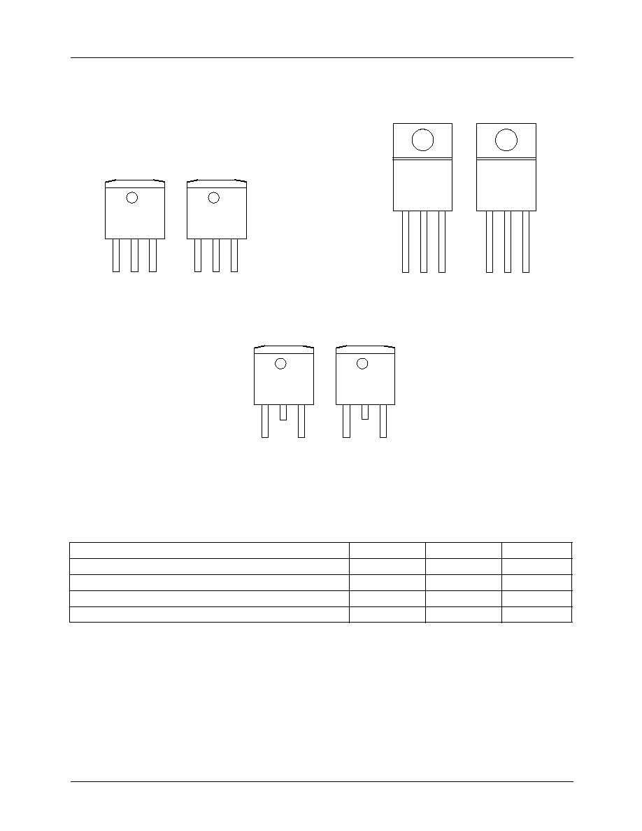
Pin Assignments
Absolute Maximum Ratings
Parameter
Min.
Max.
Unit
V
IN
7
V
Operating Junction Temperature Range
0
125
∞
C
Storage Temperature Range
-65
150
∞
C
Lead Temperature (Soldering, 10 sec.)
300
∞
C
ADJ
*
JA
can vary from 20
∞
C/W to >40
∞
C/W with various mounting techniques.
OUT
FRONT VIEW
3-Lead Plastic TO-220
JC
= 3
∞
C/W
IN
ADJ OUT
FRONT VIEW
3-Lead Plastic TO-263
JC
= 3
∞
C/W*
IN
1
2
3
1
2
3
GND OUT
FRONT VIEW
IN
1
2
3
GND OUT
FRONT VIEW
RC1584M
RC1584M-1.5
RC1584T-1.5
RC1584T
IN
1
2
3
ADJ
FRONT VIEW
3-Lead Plastic TO-263 Center Cut
JC
= 3
∞
C/W*
IN
Tab is Out.
1
2
3
GND
FRONT VIEW
RC1584MC
RC1584MC-1.5
IN
1
2
3
65-1584-02

PRODUCT SPECIFICATION
RC1584
REV. 1.0.5 7/13/00
3
Electrical Characteristics
Tj = 25∞C unless otherwise specified.
The
∑
denotes specifications which apply over the specified operating temperature range.
Notes:
1. See thermal regulation specifications for changes in output voltage due to heating effects. Load and line regulation are
measured at a constant junction temperature by low duty cycle pulse testing.
2. Line and load regulation are guaranteed up to the maximum power dissipation (18W). Power dissipation is determined by
input/output differential and the output currrent. Guaranteed maximum output power will not be available over the full input/
output voltage range.
3. RC1584 only.
4. RC1584-1.5 only.
Parameter
Conditions
Min.
Typ.
Max
Units
Reference Voltage
3
1.5V
(V
IN
≠ V
OUT
)
5.75V,
10mA
I
OUT
7A
∑
1.225
(-2%)
1.250
1.275
(+2%)
V
Output Voltage
4
3.3V
V
IN
7V
10mA
I
OUT
7A
∑
1.47
1.5
1.53
V
Line Regulation
1, 2
(V
OUT
+ 1.5V)
V
IN
7V,
I
OUT
=
10mA
∑
0.005
0.2
%
Load Regulation
1, 2
(V
IN
≠ V
OUT
) = 3V
10mA
I
OUT
7A
∑
0.05
0.5
%
Dropout Voltage
V
REF
= 1%, I
OUT
= 7A
∑
1.150
1.300
V
Current Limit
(V
IN
≠ V
OUT
) = 2V
∑
7.1
8
A
Adjust Pin Current
3
∑
35
120
µ
A
Adjust Pin Current Change
3
1.5V
(V
IN
≠ V
OUT
)
5.75V,
10mA
I
OUT
7A
∑
0.2
5
µ
A
Minimum Load Current
1.5V
(V
IN
≠ V
OUT
)
5.75V
∑
10
mA
Quiescent Current
V
IN
= 5V
∑
4
13
mA
Ripple Rejection
f = 120Hz, C
OUT
= 22
µ
F Tantalum,
(V
IN
≠ V
OUT
) = 3V, I
OUT
= 7A
60
72
dB
Thermal Regulation
T
A
= 25
∞
C, 30ms pulse
0.004
0.02
%/W
Temperature Stability
∑
0.5
%
Long-Term Stability
T
A
= 125
∞
C, 1000 hrs.
0.03
1.0
%
RMS Output Noise
(% of V
OUT
)
T
A
= 25
∞
C, 10Hz
f
10kHz
0.003
%
Thermal Resistance,
Junction to Case
TO-220
3
∞
C/W
TO-263
3
∞
C/W
Thermal Shutdown
150
∞
C

RC1584
PRODUCT SPECIFICATION
4
REV. 1.0.5 7/13/00
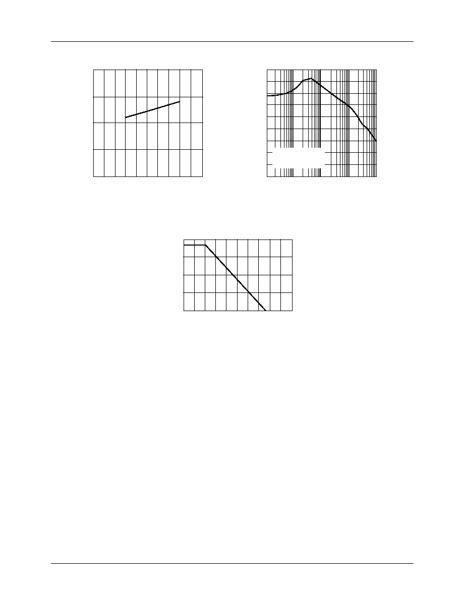
Typical Performance Characteristics
Figure 1. Dropout Voltage vs. Output Current
Figure 2. Load Regulation vs. Temperature
Figure 3. Reference Voltage vs. Temperature
Figure 4. Output Voltage vs. Temperature
Figure 5. Minimum Load Current vs. Temperature
Figure 6. Adjust Pin Current vs. Temperature
1
2
3
OUTPUT CURRENT (A)
DROPOUT VOLTAGE (V)
5
4
7
6
0
1.5
1.4
1.3
1.2
1.1
1.0
0.9
0.8
0.7
0.6
0.5
T=25
∞
C
T=0
∞
C
T=125
∞
C
65-1584-03
JUNCTION TEMPERATURE (
∞
C)
OUTPUT VOLTAGE DEVIATION (%)
-75 -50 -25
0
25
50
75 100 125 150 175
0.10
0.05
0
-0.05
-0.10
-0.15
-0.20
I = 7A
65-1584-04
JUNCTION TEMPERATURE (
∞
C)
REFERENCE VOLTAGE (V)
-75 -50 -25
0
25
50
75 100 125 150 175
1.275
1.270
1.265
1.260
1.255
1.250
1.245
1.240
1.235
1.230
1.225
65-1584-05
JUNCTION TEMPERATURE (
∞
C)
REFERENCE VOLTAGE (V)
-75 -50 -25
0
25
50
75 100 125 150 175
3.70
3.65
3.60
3.55
3.50
3.45
3.40
3.35
3.30
3.25
3.20
V
OUT
SET WITH 1% RESISTORS
V
OUT
= 3.6V
1
Note:
1. RC1584 Only
65-1584-06
JUNCTION TEMPERATURE (
∞
C)
MINIMUM LOAD CURRENT (mA)
-75 -50 -25
0
25
50
75 100 125 150 175
5
4
3
2
1
0
65-1584-07
JUNCTION TEMPERATURE (
∞
C)
ADJUST PIN CURRENT (
µ
A)
-75 -50 -25
0
25
50
75 100 125 150 175
100
90
80
70
60
50
40
30
20
10
0
65-1584-08
Note:
1. RC1584 Only
PRODUCT SPECIFICATION
RC1584
REV. 1.0.5 7/13/00
5
Typical Performance Characteristics
(continued)
Figure 7. Short-Circuit Current vs. Temperature
Figure 8. Ripple Rejection vs. Frequency
Figure 9. Maximum Power Dissipation
FREQUENCY (Hz)
RIPPLE REJECTIONS (dB)
10
100
1K
10K
100K
90
80
70
60
50
40
30
20
10
0
65-1584-10
(V
IN
≠ V
OUT
)
3V
0.5V
V
RIPPLE
2V
I
OUT
= 7A
JUNCTION TEMPERATURE (
∞
C)
SHORT-CIRCUIT CURRENT (A)
-75 -50 -25
0
25
50
75 100 125 150 175
10
9
8
7
6
65-1584-09
CASE TEMPERATURE (
∞
C)
POWER (W)
50
60
70
80
90 100 110 120 130 140 150
20
15
10
5
0
65-1584-11