www.fairchildsemi.com
Features
∑ Powered from the AC line
∑ Built-in bridge rectifier
∑ Direct interface to SCR
∑ 350
mA quiescent current
∑ Adjustable trip current
∑ Adjustable time delay
∑ Minimum external components
∑ Meets UL 943 requirements
∑ Specifically for two-wire systems
∑ For use with 110V or 220V systems
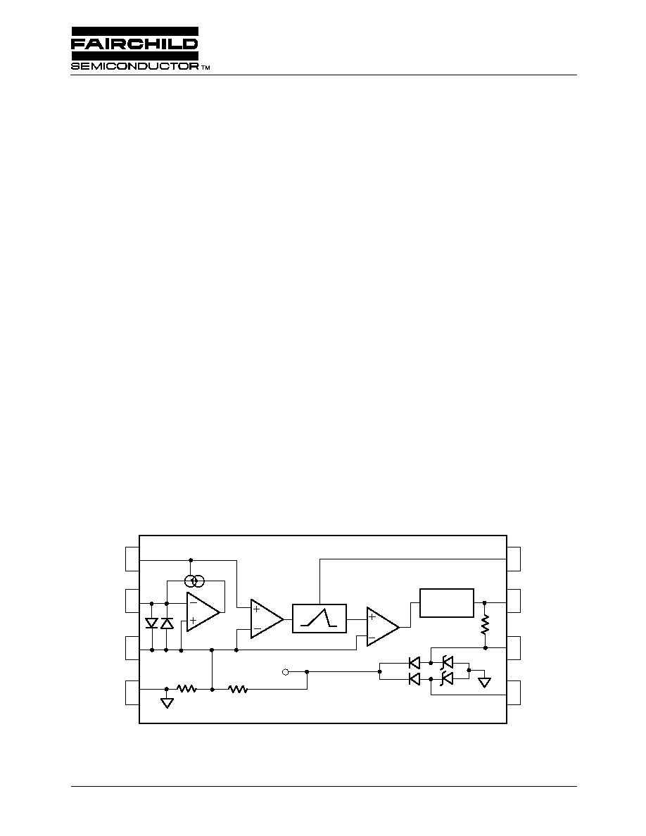
Block Diagram
65-4140A-01
1
2
3
4
8
7
6
5
Latch
4.7K
Delay
Vcc
RV4140A
RV4140A
Low Power Two-Wire Ground Fault
Interrupter Controller
Rev. 1.0.0
Description
The RV4140A is a low power controller for AC outlet
appliance leakage circuit interrupters. These devices detect
hazardous current paths to ground such as an appliance
falling into water. The interrupter then open circuits the line
before a harmful or lethal shock occurs.
Internally, the RV4140A has a diode bridge rectifier, zener
shunt regulator, op amp, current reference, time delay circuit,
latch and SCR driver.
An external sense transformer, SCR, relay, two resistors
and three capacitors complete the design of the circuit
interrupter. The simple layout and minimum component
count ensure ease of application and long term reliability.

RV4140A
PRODUCT SPECIFICATION
2
Functional Description
(Refer to Block Diagram and Figure 1 )
The shunt regulator generated by a 6.5V zener diode is
built into the internal bridge rectifier. It is divided to create
an internal reference voltage of 2.9V connected to pin 3.
The secondary of the sense transformer is AC coupled to the
inverting input of the sense amplifier at pin 2; the non-invert-
ing input is referenced to pin 3. A current feedback loop
around the sense amplifier ensures a virtual ground will be
presented to the secondary of the sense transformer. In this
manner it acts as a current transformer instead of a voltage
transformer. In this mode, the transformer's characteristics
are very predictable and circuit adjustments are not neces-
sary in production.
The sense transformer has a toroidal core made of laminated
steel rings or solid ferrite material. The secondary of the
transformer is 500 to 1000 turns of #40 wire wound through
the toroid. The primary's one turn made by passing the
AC hot and neutral wires through the center of the toroid.
When a ground fault exists, a difference exists between the
current flowing in hot and neutral wires. The difference
primary current, divided by the number of secondary turns,
flows through the secondary wire of the transformer.
The AC coupled transformer secondary current then flows
through the sense amplifier's feedback loop, creating a full
wave rectified version of the secondary fault current. This
current passes through R
SET
at pin 1, generating a voltage
equal to R
SET
times the peak fault current divided by the
sense transformer turns ratio. This voltage is compared with
the reference voltage at pin 3.
If the voltage at pin 1 is greater than pin 3, a comparator will
charge C2 through a 29
mA current source at pin 8. If the
voltage at pin 1 exceeds pin 3 for longer than the delay time,
a 400
mA current will pulse between pins 7 and 6 which will
trigger the gate of the SCR.
If the voltage at pin 1 exceeds pin 3 for less than the delay
time, the SCR will not trigger.
The fault current at which the controller triggers the SCR
is dependent on the value of R
SET
and the time delay
determined by C2.
UL 943 requires the circuit interrupter trip when the ground
fault exceeds 6 mA and not trip when the fault current is less
than 4 mA.
Supply Current Requirements
The RV4140A has a built-in diode bridge rectifier that
provides power to the chip independent of the polarity of
the AC line. This eliminates the external rectifier required for
previous GFCI controllers.
R
LlNE
limits the shunt regulator current to 2 mA. The rec-
ommended value is 47K to 91K for 110V systems and 91K
to 150K for 220V systems. The recommended maximum
peak line current through R
LlNE
is 7 mA.
DO NOT connect a filter capacitor between pins 5 and 6 in
an attempt to filter the supply voltage at the RV4140A.
Proper operaton of the RV4140A requires the internal supply
voltage to be unfiltered.
SCR Driver
The SCR must have a high dV/dt rating to ensure that line
noise (generated by electrically noisy appliances) does not
falsely trigger the SCR. Also, the SCR must have a gate drive
requirement less than 200
mA. C3 is a noise filter that
prevents high frequency line pulses from triggering the SCR.
The relay solenoid used should have a 3 ms or less response
time to meet the UL 943 timing requirement.
Supplier of Sense Transformers and Cores
Magnetic Metals Corporation, Camden, NJ 08101,
(609) 964-7842, supplies a full line of ring cores and trans-
formers designed specifically for GFCI and related applica-
tions.
Determining the Values of RSET and C2
Determine the ground fault trip current requirement. This
will be typically 5 mA in North America (117 VAC) and
10 mA in the UK and Europe.
Determine the minimum amount of time delay required to
prevent nuisance tripping. This will typically be 1 to 2 ms.
The value of C2 required to provide the desired delay time
is:
C2 = 10 x T
where C2 is in nF, and T is the desired delay time in ms.

PRODUCT SPECIFICATION
RV4140A
3
The value of R
SET
to meet nominal ground fault tip current
specification is:
Where:
∑ R
SET
is in k
W
∑ T is the time delay in ms
∑ P is the period of the line frequency in ms
∑ I
FAULT
is the desired ground fault trip current in mA
RMS.
∑ N is the number of sense transformer secondary turns.
This formula assumes an ideal sense transformer is used.
The calculated value of R
SET
may have to be changed up to
30% when using a non-ideal transformer.
Figure 1. Appliance Leakage Detector Circuit Application
R
SET
2.05
N
¥
I
FAULT
COS 180
¥
T P
§
(
)
---------------------------------------------------------------
=
65-4140A-02
Closed
Contacts
Load
Solinoid
C3
10 nF
Q1
Tag
X0103DA
R
LINE
C2
0.02 F
m
1
2
3
4
8
7
6
5
R
SET
C1
10 F
Hot
Neutral
Line
Sense Transformer
1:500 Turns Ratio
3 Ring Steel Core
RV4140A
m
Normally
Latching
Mov
R
TEST
C4
0.1 F
m
Press to Test
15K
191K
91K