Äîêóìåíòàöèÿ è îïèñàíèÿ www.docs.chipfind.ru
© 2000 Fairchild Semiconductor Corporation
DS010963
www.fairchildsemi.com
October 1991
Revised May 2000
SCAN18374
T D-
T
y
p
e
Fl
ip-
F
l
op wit
h
3-ST
A
T
E Out
puts
SCAN18374T
D-Type Flip-Flop with 3-STATE Outputs
General Description
The SCAN18374T is a high speed, low-power D-type flip-
flop featuring separate D-type inputs organized into dual 9-
bit bytes with byte-oriented clock and output enable control
signals. This device is compliant with IEEE 1149.1 Stan-
dard Test Access Port and BOUNDARY-SCAN Architec-
ture with the incorporation of the defined BOUNDARY-
SCAN test logic and test access port consisting of Test
Data Input (TDI), Test Data Out (TDO), Test Mode Select
(TMS), and Test Clock (TCK).
Features
s
IEEE 1149.1 (JTAG) Compliant
s
Buffered positive edge-triggered clock
s
3-STATE outputs for bus-oriented applications
s
9-bit data busses for parity applications
s
Reduced-swing outputs source 32 mA/sink 64 mA
s
Guaranteed to drive 50
transmission line to TTL input
levels of 0.8V and 2.0V
s
TTL compatible inputs
s
25 mil pitch SSOP (Shrink Small Outline Package)
s
Includes CLAMP and HIGHZ instructions
s
Member of Fairchild's SCAN Products
Ordering Code:
Devices also available in Tape and Reel. Specify by appending the suffix letter "X" to the ordering code.
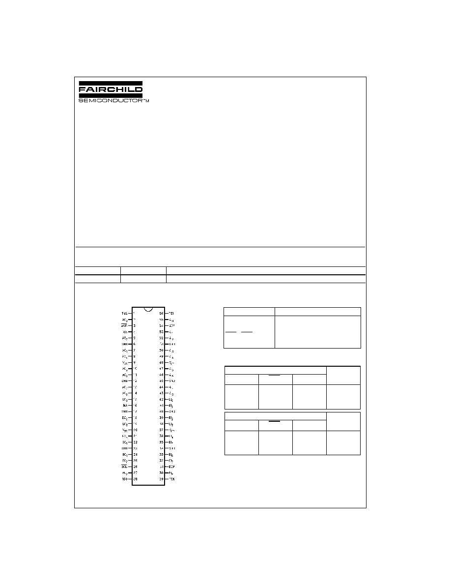
Connection Diagram
Pin Descriptions
Truth Tables
H
=
HIGH Voltage Level
L
=
LOW Voltage Level
X
=
Immaterial
Z
=
High Impedance
=
L-to-H Transition
Order Number
Package Number
Package Description
SCAN18374TSSC
MS56A
56-Lead Shrink Small Outline Package (SSOP), JEDEC MO-118, 0.300 Wide
Pin Names
Description
AI
(08)
, BI
(08)
Data Inputs
ACP, BCP
Clock Pulse Inputs
AOE
1
, BOE
1
3-STATE Output Enable Inputs
AO
(08)
, BO
(08)
3-STATE Outputs
Inputs
AO
(08)
ACP
AOE
1
AI
(08)
X
H
X
Z
L
L
L
L
H
H
Inputs
BO
(08)
BCP
BOE
1
BI
(08)
X
H
X
Z
L
L
L
L
H
H
www.fairchildsemi.com
2
SCAN18374
T
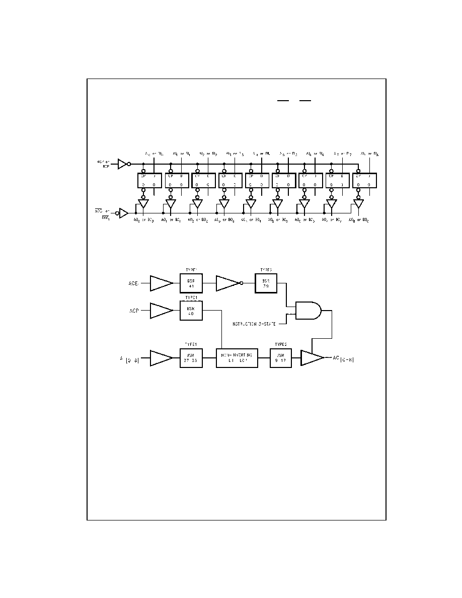
Functional Description
The SCAN18374 consists of two sets of nine edge-trig-
gered flip-flops with individual D-type inputs and 3-STATE
true outputs. The buffered clock and buffered Output
Enable pins are common to all flip-flops. Each set of the
nine flip-flops will store the state of their individual D inputs
that meet the setup and hold time requirements on the
LOW-to-HIGH Clock (ACP or BCP) transition. With the
Output Enable (AOE
1
or BOE
1
) LOW, the contents of the
nine flip-flops are available at the outputs. When the Output
Enable is HIGH, the outputs go to the high impedance
state. Operation of the Output Enable input does not affect
the state of the flip-flops.
Logic Diagram
Please note that this diagram is provided only for the understanding of logic operations and should not be used to estimate propagation delays.
Block Diagrams
Byte-A
Note: BSR stands for Boundary Scan Register
3
www.fairchildsemi.com
SCAN18374
T
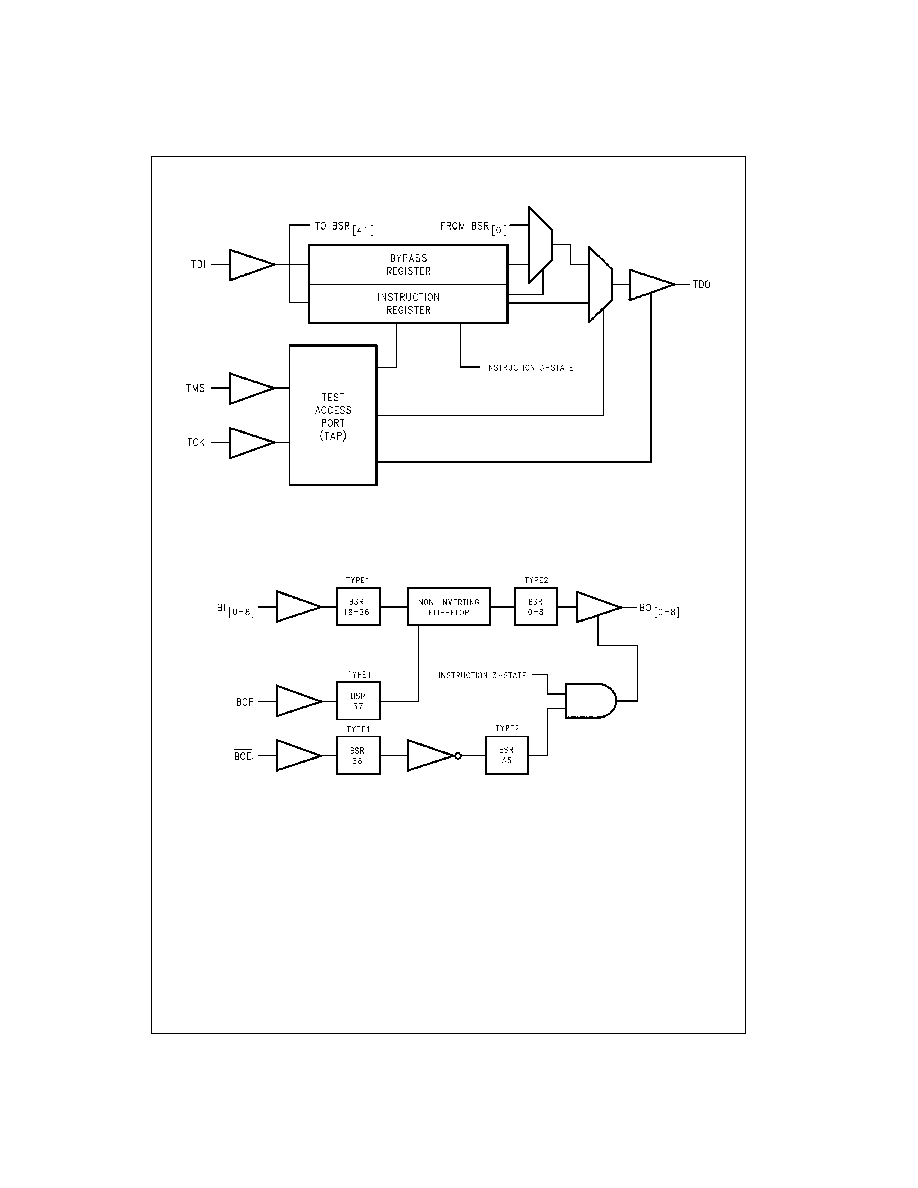
Block Diagrams
(Continued)
Tap Controller
Byte-B
Note: BSR stands for Boundary Scan Register
www.fairchildsemi.com
4
SCAN18374
T
Description of Boundary-Scan Circuitry
The scan cells used in the BOUNDARY-SCAN register are
one of the following two types depending upon their loca-
tion. Scan cell TYPE1 is intended to solely observe system
data, while TYPE2 has the additional ability to control sys-
tem data.
Scan cell TYPE1 is located on each system input pin while
scan cell TYPE2 is located at each system output pin as
well as at each of the two internal active-high output enable
signals. AOE controls the activity of the A-outputs while
BOE controls the activity of the B-outputs. Each will acti-
vate their respective outputs by loading a logic high.
The BYPASS register is a single bit shift register stage
identical to scan cell TYPE1. It captures a fixed logic low.
Bypass Register Scan Chain Definition
Logic 0
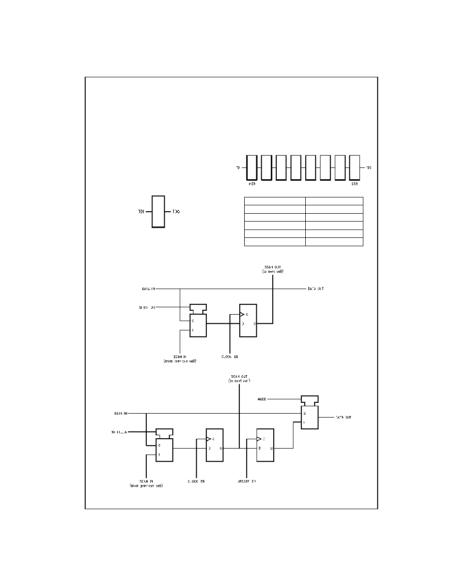
The INSTRUCTION register is an eight-bit register which
captures the value 00111101.
The two least significant bits of this captured value (01) are
required by IEEE Std 1149.1. The upper six bits are unique
to the SCAN18374T device. SCAN CMOS Test Access
Logic devices do not include the IEEE 1149.1 optional
identification register. Therefore, this unique captured
value can be used as a "pseudo ID" code to confirm that
the correct device is placed in the appropriate location in
the boundary scan chain.
Instruction Register Scan Chain Definition
MSB
LSB
Scan Cell TYPE1
Scan Cell TYPE2
Instruction Code
Instruction
00000000
EXTEST
10000001
SAMPLE/PRELOAD
10000010
CLAMP
00000011
HIGHZ
All Others
BYPASS
5
www.fairchildsemi.com
SCAN18374
T
Description of Boundary-Scan Circuitry
(Continued)
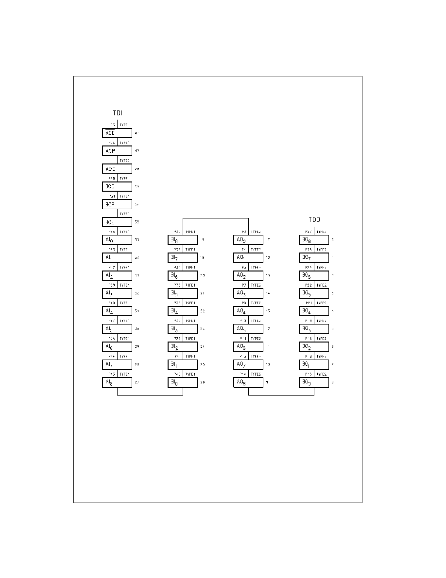
Boundary-Scan Register
Scan Chain Definition (42 Bits in Length)