FEATURES
* High Speed Switching
* Low Saturation Voltage
: V
CE
(sat) = 1.95 V (@ Ic=12A)
* High Input Impedance
APPLICATIONS
* AC & DC Motor controls
* General Purpose Inverters
* Robotics , Servo Controls
* Power Supply
* Lamp Ballast
ABSOLUTE MAXIMUM RATINGS
Notes:
(1) Repetitive rating : Pulse width limited by max. junction temperature
Symbol
V
CES
V
GES
I
C
I
CM (1)
P
C
Tj
Tstg
T
L
Characteristics
Collector-Emitter Voltage
Gate-Emitter Voltage
Collector Current @ Tc = 25
°
C
Collector Current @ Tc = 100
°
C
Pulsed Collector Current
Maximum Power Dissipation @Tc = 25
°
C
Maximum Power Dissipation @Tc = 100
°
C
Operating Junction Temperature
Storage Temperature Range
Maximum Lead Temp. For Soldering
Purposes, 1/8
"
from case for 5 seconds
Rating
600
±
20
23
12
92
100
40
-55 ~ 150
-55 ~ 150
300
Units
V
V
A
A
A
W
W
°
C
°
C
°
C
G
C
E
TO-3P
SGH23N60UF
N-CHANNEL IGBT
©
1999 Fairchild Semiconductor Corporation
Rev.B
ELECTRICAL CHARACTERISTICS
(T
c
=25
°
C,Unless Otherwise Specified)
Characteristics
C - E Breakdown Voltage
Temperature Coeff. of
Breakdown Voltage
G - E threshold voltage
Collector cutoff Current
G - E leakage Current
Collector to Emitter
saturation voltage
Input capacitance
Output capacitance
Reverse transfer capacitance
Turn on delay time
Turn on rise time
Turn off delay time
Turn off fall time
Turn on Switching Loss
Turn off Switching Loss
Total Switching Loss
Total Gate Charge
Gate-Emitter Charge
Gate-Collector Charge
Internal Emitter Inductance
Symbol
BV
CES
V
CES/
T
J
V
GE(th)
I
CES
I
GES
V
CE
(sat)
Cies
Coes
Cres
td(on)
tr
td(off)
tf
Eon
Eoff
Ets
Qg
Qge
Qgc
Le
Min
600
-
4.0
-
-
-
-
-
-
-
-
-
-
-
-
-
-
-
-
-
-
Typ
-
0.6
5.5
-
-
1.95
2.6
720
65
26
12
20
55
100
0.11
0.19
0.3
48
11
14
7.5
Max
-
-
7.5
250
100
2.6
-
-
-
-
-
-
85
220
-
-
0.5
72
16
21
-
Units
V
V/
°
C
V
uA
nA
V
V
pF
pF
pF
ns
ns
ns
ns
mJ
mJ
mJ
nC
nC
nC
nH
Test Conditions
V
GE
= 0V , I
C
= 250uA
V
GE
= 0V , I
C
= 1mA
I
C
= 12mA , V
CE
= V
GE
V
CE
= V
CES
, V
GE
= 0V
V
GE
= V
GES
, V
CE
= 0V
Ic=12A, V
GE
= 15V
Ic=23A, V
GE
= 15V
V
GE
= 0V , f = 1MHz
V
CE
= 30V
V
CC
= 300V , I
C
= 12A
V
GE
= 15V
R
G
= 23
Inductive Load
Vcc = 300V
V
GE
= 15V
Ic = 12A
Measured 5mm from PKG
SGH23N60UF
N-CHANNEL IGBT
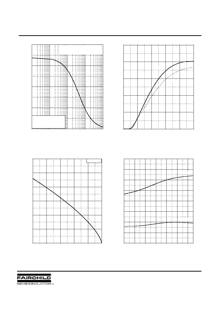
Fig.1 Typical Load Current vs. Frequency
Fig.2 Typical Output Characteristics
Fig.3 Maximum Collector Current vs.
Case Temperature
Fig.4 Collector to Emitter Voltage vs.
Case Temperature
20
40
60
80
100
120
140
1.6
1.8
2.0
2.2
2.4
2.6
2.8
3.0
3.2
Ic = 12A
Ic = 23A
V
c
e
(
s
a
t)
[V
]
Tc [
]
0
2
4
6
8
10
0
20
40
60
80
100
Tc = 100
Tc = 25
Ic
[
A
]
Vce [V]
0
5
10
15
20
25
30
25
50
75
100
125
150
Vge = 15V
Tc [
]
M
a
x
DC
Cu
r
r
e
n
t
[
A
]
0
5
10
15
20
0.1
1
10
100
1000
Duty cycle : 50%
Tc = 100
Power Dissipation = 21W
Vcc = 300V
Load Current : peak of square wave
Frequency [kHz]
Load C
u
r
r
en
t
[
A
]
SGH23N60UF
N-CHANNEL IGBT
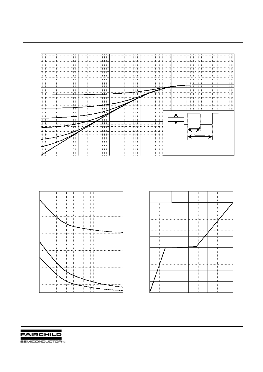
Fig.5 Maximum Effective Transient Thermal Impedance, Junction to Case
Fig.6 Typical Capacitance vs.
Collector to Emitter Voltage
Fig.7 Typical Gate Charge vs.
Gate to Emitter Voltage
1
10
0
200
400
600
800
1000
1200
Cres
Coes
Cies
Ca
p
a
c
i
t
a
n
c
e
[
p
F
]
Vce [V]
0
10
20
30
40
0
2
4
6
8
10
12
14
16
18
Vcc = 300V
Ic = 12A
V
GE
[V
]
Qg [nC]
0 .0 0 0 0 1
0 .0 0 0 1
0 .0 0 1
0 .0 1
0 .1
1
1 0
0 .0 1
0 .1
1
1 0
0 .5
0 .2
0 .1
0 .0 5
0 .0 2
0 .0 1
s i n g l e p u l s e
T
her
m
a
l
R
e
s
pons
e [
Z
t
h
j
c
]
Rectangular Pulse Duration [sec]
Pdm
t1
t2
Duty factor D = t1 / t2
Peak Tj = Pdm x Zthjc + Tc
SGH23N60UF
N-CHANNEL IGBT