 | ÐлекÑÑоннÑй компоненÑ: SGU15N40L | СкаÑаÑÑ:  PDF PDF  ZIP ZIP |
Äîêóìåíòàöèÿ è îïèñàíèÿ www.docs.chipfind.ru
©2002 Fairchild Semiconductor Corporation
SGR15N40L / SGU15N40L Rev. A1
IGBT
S
G
R15N40L /
SGU15N40L
SGR15N40L / SGU15N40L
General Description
Insulated Gate Bipolar Transistors (IGBTs) with a trench
gate structure provide superior conduction and switching
performance in comparison with transistors having a planar
gate structure. They also have wide noise immunity. These
devices are very suitable for strobe applications
Features
· High input impedance
· High peak current capability (130A)
· Easy gate drive
Absolute Maximum Ratings
T
C
= 25
°
C unless otherwise noted
Notes :
(1) Repetitive rating : Pulse width limited by max. junction temperature
Thermal Characteristics
Notes :
(2) Mounted on 1" square PCB (FR4 or G-10 Material)
Symbol
Description
SGR / SGU15N40L
Units
V
CES
Collector - Emitter Voltage
400
V
V
GES
Gate - Emitter Voltage
±
6
V
I
CM (1)
Pulsed Collector Current
130
A
P
C
Maximum Power Dissipation @ T
C
= 25
°
C
45
W
T
J
Operating Junction Temperature
-40 to +150
°
C
T
stg
Storage Temperature Range
-40 to +150
°
C
T
L
Maximum Lead Temp. for soldering
purposes, 1/8" from case for 5 seconds
300
°
C
Symbol
Parameter
Typ.
Max.
Units
R
JC
Thermal Resistance, Junction-to-Case
--
3.0
°
C
/
W
R
JA
(D-PAK)
Thermal Resistance, Junction-to-Ambient (PCB Mount)
(2)
--
50
°
C
/
W
R
JA
(I-PAK)
Thermal Resistance, Junction-to-Ambient
--
110
°
C
/
W
Application
Strobe flash.
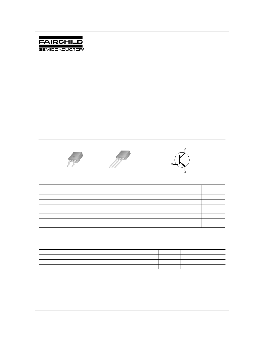
G
C
E
G
C
E
D-PAK
G E
C
I-PAK
G
E
C
SGR15N40L / SGU15N40L Rev. A1
S
G
R15N40L /
SGU15N40L
©2002 Fairchild Semiconductor Corporation
Electrical Characteristics of the IGBT
T
C
= 25
°
C unless otherwise noted
* Notes : Recommendation of R
G
Value : R
G
15
Symbol
Parameter
Test Conditions
Min.
Typ.
Max.
Units
Off Characteristics
BV
CES
Collector - Emitter Breakdown Voltage
V
GE
= 0V, I
C
= 1mA
450
--
--
V
I
CES
Collector Cut-Off Current
V
CE
= V
CES
, V
GE
= 0V
--
--
10
uA
I
GES
G - E Leakage Voltage
V
GE
= V
GES
, V
CE
= 0V
--
--
±
0.1
uA
On Characteristics
V
GE(th)
G - E Threshold Voltage
I
C
= 1mA, V
CE
= V
GE
0.5
1.0
1.4
V
V
CE(sat)
C - E Saturation Current
I
C
= 130A, V
GE
= 4.5V
2.0
4.5
8.0
V
Dynamic Characteristics
C
ies
Input Capacitance
V
GE
= 0V, V
CE
= 30V,
f = 1MHz
--
3000
--
pF
C
oes
Output Capacitance
--
45
--
pF
C
res
Reverse Transfer Capacitance
--
30
--
pF
Switching Characteristics
t
d(on)
Turn-On Delay Time
V
CC
= 300V, I
C
= 130A,
V
GE
= 4.5V, R
G
= 15
Resistive Load
--
0.08
--
us
t
r
Rise Time
--
1.4
--
us
t
d(off)
Turn-Off Delay Time
--
0.1
0.5
us
t
f
Fall Time
--
1.1
2.0
us
SGR15N40L / SGU15N40L Rev. A1
S
G
R15N40L /
SGU15N40L
©2002 Fairchild Semiconductor Corporation
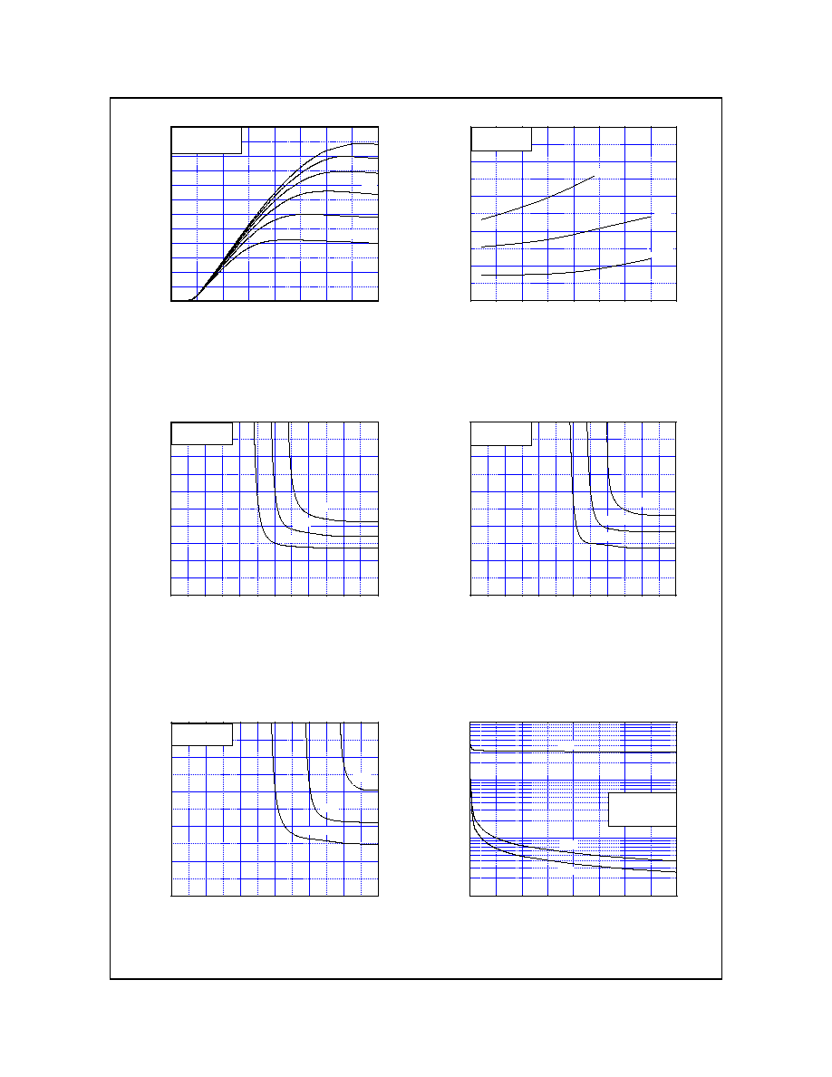
Fig 1. Typical Output Characteristics
Fig 2. Saturation Voltage vs. Case Temperature
at Variant Current Level
Fig 3. Saturation Voltage vs. V
GE
Fig 4. Saturation Voltage vs. V
GE
Fig 5. Saturation Voltage vs. V
GE
Fig 6. Capacitance Characteristics
0
2
4
6
8
0
30
60
90
120
150
180
4V
4.5V
3V
3.5V
5V
V
GE
= 2.5V
Commom Emitter
T
C
= 25
C
o
llec
t
or C
u
rrent, I
C
[A]
Collector-Emitter Voltage, V
CE
[V]
-50
0
50
100
150
2
3
4
5
6
7
Common Emitter
V
GE
= 4.5V
130A
100A
I
C
= 70A
Collector-Em
i
tter Voltag
e, V
CE
[V]
Case Temperature, T
C
[
]
0
1
2
3
4
5
6
0
2
4
6
8
10
130A
100A
I
C
= 70A
Common Emitter
T
C
= -40
C
o
llecto
r-Em
i
tter Vo
ltag
e,
V
CE
[V
]
Gate-Emitter Voltage , V
GE
[V]
0
1
2
3
4
5
6
0
2
4
6
8
10
Common Emitter
T
C
= 25
130A
100A
I
C
= 70A
Collector-Em
i
tter Voltag
e, V
CE
[V]
Gate-Emitter Voltage, V
GE
[V]
0
1
2
3
4
5
6
0
2
4
6
8
10
130A
100A
I
C
= 70A
Common Emitter
T
C
= 125
Co
llector-E
m
i
tter V
o
ltag
e,
V
CE
[V
]
Gate-Emitter Voltage, V
GE
[V]
0
10
20
30
40
10
100
1000
10000
Common Emitter
V
GE
= 0V, f = 1MHz
T
C
= 25
Cres
Coes
Cies
Ca
p
a
citan
ce [p
F]
Collector-Emitter Voltage, V
CE
[V]
SGR15N40L / SGU15N40L Rev. A1
S
G
R15N40L /
SGU15N40L
©2002 Fairchild Semiconductor Corporation
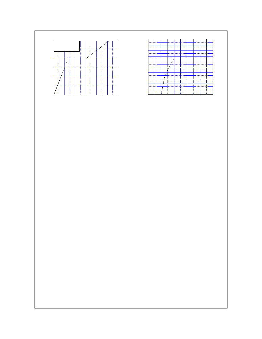
Fig 7. Gate Charge Characteristics
Fig 8. Collector Current Limit vs.
Gate - Emitter Voltage Limit
0
10
20
30
40
50
60
0
2
4
6
Common Emitter
V
CC
= 300V, R
L
= 2.2
T
C
= 25
G
a
te - E
m
itter V
o
ltag
e, V
GE
[V
]
Gate Charge, Q
g
[nC]
0
2
4
6
8
10
0
20
40
60
80
100
120
140
160
180
200
Collector Peak
C
u
rren
t, I
CP
[A]
Gate-Emitter Voltage, V
GE
[V]
©2002 Fairchild Semiconductor Corporation
SGR15N40L / SGU15N40L Rev. A1
S
G
R15N40L /
SGU15N40L
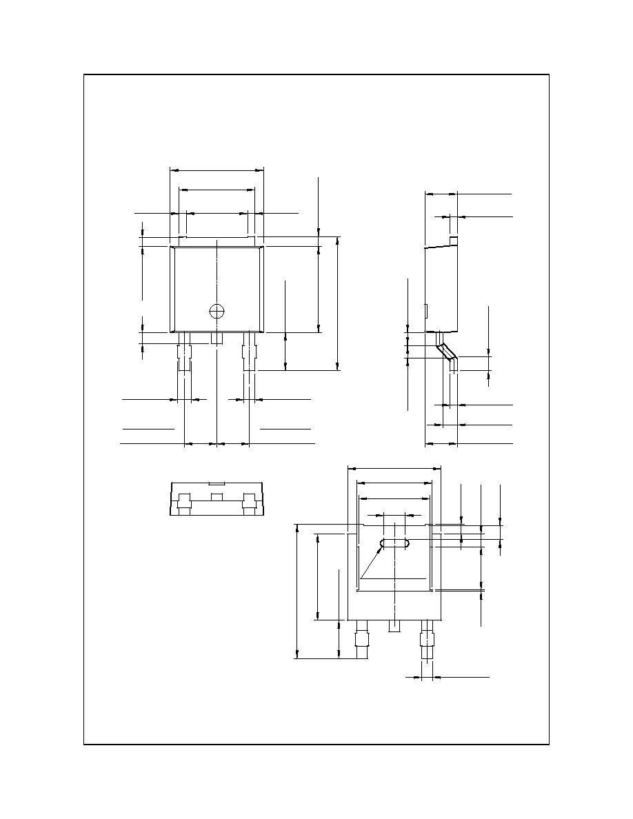
Package Dimension
6.60
±
0.20
2.30
±
0.10
0.50
±
0.10
5.34
±
0.30
0.70
±
0.20
0.60
±
0.20
0.80
±
0.20
9.50
±
0.30
6.10
±
0.20
2.70
±
0.20
9.50
±
0.30
6.10
±
0.20
2.70
±
0.20
MIN0.55
0.76
±
0.10
0.50
±
0.10
1.02
±
0.20
2.30
±
0.20
6.60
±
0.20
0.76
±
0.10
(5.34)
(1.50)
(2XR0.25)
(5.04)
0.89
±
0.10
(0.10)
(3.05)
(1.00)
(0.90)
(0.70)
0.91
±
0.10
2.30TYP
[2.30
±
0.20]
2.30TYP
[2.30
±
0.20]
MAX0.96
(4.34)
(0.50)
(0.50)
D-PAK
Dimensions in Millimeters