 | –≠–ª–µ–∫—Ç—Ä–æ–Ω–Ω—ã–π –∫–æ–º–ø–æ–Ω–µ–Ω—Ç: SPT9689 | –°–∫–∞—á–∞—Ç—å:  PDF PDF  ZIP ZIP |

SPT9689
DUAL ULTRAFAST VOLTAGE COMPARATOR
TECHNICAL DATA
FEBRUARY 20, 2001
FEATURES
∑ 650 ps propagation delay
∑ 100 ps propagation delay variation
∑ 70 dB CMRR
∑ Low feedthrough and crosstalk
∑ Differential latch control
∑ ECL compatible
APPLICATIONS
∑ Automated test equipment
∑ High-speed instrumentation
∑ Window comparators
∑ High-speed timing
∑ Line receivers
∑ High-speed triggers
∑ Threshold detection
∑ Peak detection
GENERAL DESCRIPTION
The SPT9689 is a
Subnanosecond monolithic dual com-
parator. The propagation delay variation is less than
100 ps from 5 to 50 mV input overdrive voltage. The input
slew rate is 10 V/ns. The device utilizes a high precision
differential input stage with a common-mode range of
≠2.5 V to +4.0 V.
ECL-compatible complementary digital outputs are ca-
pable of driving 50
terminated transmission lines and
providing 30 mA output drive. The SPT9689 is pin compat-
ible with the SPT9687. It is available in 20-lead PLCC and
20-contact LCC packages over the industrial temperature
range. The SPT9689 is also available in die form.
BLOCK DIAGRAM
A
+
INVERTING
INPUT
GND
A
LATCH ENABLE
LATCH ENABLE
Q OUTPUT
Q OUTPUT
INVERTING
INPUT
NONINVERTING
INPUT
GND
B
LATCH ENABLE
LATCH ENABLE
Q OUTPUT
Q OUTPUT
NONINVERTING
INPUT
+
B
V
EE
V
CC
2
2/20/01
SPT9689
ABSOLUTE MAXIMUM RATINGS (Beyond which damage may occur)
1
25 ∞C
Note: 1. Operation at any Absolute Maximum Rating is not implied. See
Electrical Specifications for proper nominal applied conditions
in typical applications.
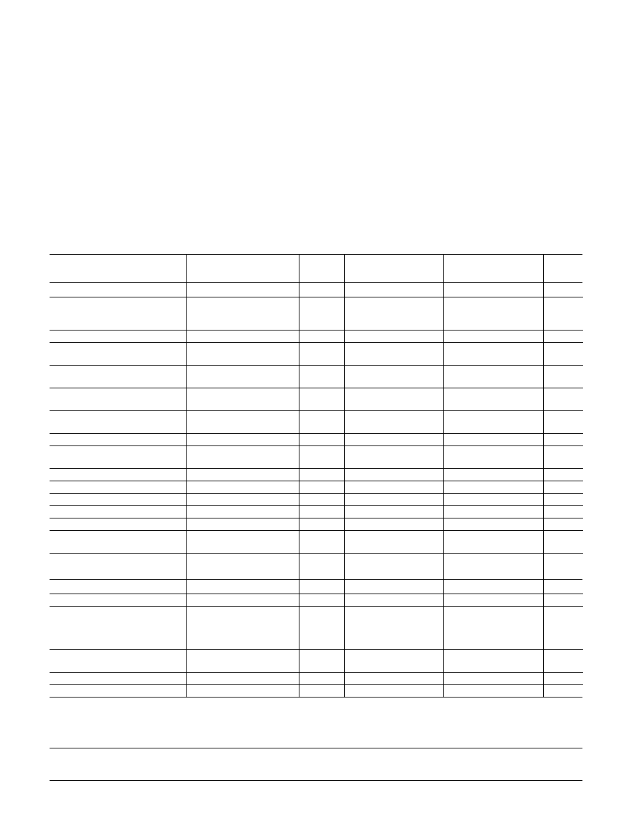
ELECTRICAL SPECIFICATIONS
T
A
= +25 ∞C, V
CC
= +5.0 V, V
EE
=≠5.20 V, R
L
= 50 Ohm to ≠2 V, unless otherwise specified.
TEST
TEST
SPT9689A
SPT9689B
PARAMETERS
CONDITIONS
LEVEL
MIN
TYP
MAX
MIN
TYP
MAX
UNITS
DC CHARACTERISTICS
Input Offset Voltage
V
IN
,
CM
=0, R
S
=0 Ohms
1
I
≠10
±3.0
10
≠25
±12
25
mV
Input Offset Voltage
V
IN
,
CM
=0, R
S
=0 Ohms
1
T
MIN
<T
A
<T
MAX
IV
≠15
±4.5
15
≠30
±15
30
mV
Offset Voltage Tempco
V
10
40
µV/∞C
Input Bias Current
I
±8
±25
±8
±25
µA
Input Bias Current
T
MIN
<T
A
<T
MAX
IV
±12
±38
±12
±38
µA
Input Offset Current
I
±1.0
±3.0
±2.0
±5.0
µA
Input Offset Current
T
MIN
<T
A
<T
MAX
IV
±2.0
±5.0
±4.0
±7.0
µA
Positive Supply Current
Dual
I
18
30
18
35
mA
Negative Supply Current
Dual
I
40
55
40
60
mA
Positive Supply Voltage, V
CC
IV
4.75
5.0
5.25
4.75
5.0
5.25
V
Negative Supply Voltage, V
EE
IV
≠4.95
≠5.2 ≠5.45
≠4.95
≠5.2
≠5.45
V
Input Common Mode Range
V
≠2.5
+4.0
≠2.5
+4.0
V
Latch Enable
Common Mode Range
IV
≠2.0
0
≠2.0
0
V
Open Loop Gain
V
66
66
dB
Differential Input Resistance
V
500
500
k
Input Capacitance
V
0.6
0.6
pF
Power Supply Sensitivity
V
70
70
dB
Common Mode Rejection Ratio
V
CM
=≠2.5 to +4.0
V
70
70
dB
Power Dissipation
Dual, Without Load
I
350
425
350
475
mW
Power Dissipation
Dual, With Load
I
400
550
400
550
mW
Output High Level
ECL 50 Ohms to ≠2 V
I
≠1.00
≠.81
≠1.00
≠.81
V
Output Low Level
ECL 50 Ohms to ≠2 V
I
≠1.95
≠1.54
≠1.95
≠1.54
V
AC CHARACTERISTICS
Propagation Delay
20 mV O.D.
IV
650
850
750
950
ps
Latch Set-up Time
V
150
300
150
300
ps
Latch to Output Delay
250 mV O.D.
V
500
600
500
600
ps
Latch Pulse Width
V
500
500
ps
Latch Hold Time
V
0
0
ps
Rise Time
20% to 80%
V
180
180
ps
Fall Time
20% to 80%
V
80
80
ps
Slew Rate
V
10
10
V/ns
Bandwidth
≠3 dB
V
900
900
MHz
1
R
S
= Source impedance
Supply Voltages
Positive Supply Voltage (V
CC
to GND) .... ≠0.5 to +6.0 V
Negative Supply Voltage (V
EE
to GND) .. ≠6.0 to +0.5 V
Ground Voltage Differential .................... ≠0.5 to +0.5 V
Input Voltages
Input Common Mode Voltage ................. ≠4.0 to +5.0 V
Differential Input Voltage ........................ ≠3.0 to +3.0 V
Input Voltage, Latch Controls .................... V
EE
to 0.5 V
Output
Output Current ................................................... 30 mA
Temperature
Operating Temperature, ambient ............ ≠40 to +85 ∞C
junction ..................... +150 ∞C
Lead Temperature, (soldering 60 seconds) ..... +300 ∞C
Storage Temperature ............................ ≠65 to +150 ∞C
3
2/20/01
SPT9689
V
IN
+=100 mV (p-p), V
OD
=20 mV
V
REF
± V
OS
50%
50%
50%
t
t
t
pL
t
t
Differential
Input Voltage
Output Q
Output Q
t
S
t
H
pdL
pdH
pLOL
pLOH
Latch Enable
Latch Enable
V
OD
TEST LEVEL CODES
All electrical characteristics are subject to the
following conditions:
All parameters having min/max specifications
are guaranteed. The Test Level column indi-
cates the specific device testing actually per-
formed during production and Quality Assur-
ance inspection. Any blank section in the data
column indicates that the specification is not
tested at the specified condition.
LEVEL
TEST PROCEDURE
I
100% production tested at the specified temperature.
II
100% production tested at T
A
= +25 ∞C, and sample tested at the
specified temperatures.
III
QA sample tested only at the specified temperatures.
IV
Parameter is guaranteed (but not tested) by design and characteri-
zation data.
V
Parameter is a typical value for information purposes only.
VI
100% production tested at T
A
= +25 ∞C. Parameter is guaranteed
over specified temperature range.
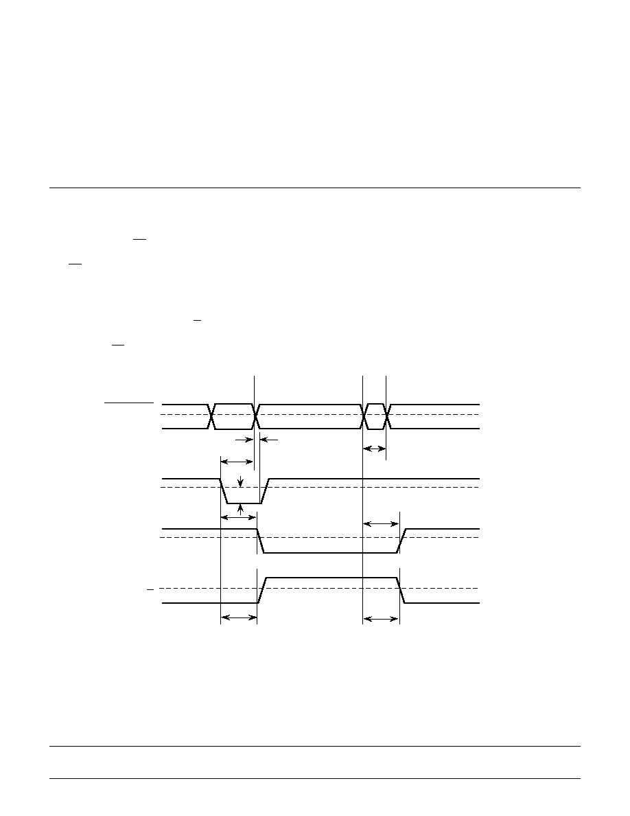
TIMING INFORMATION
The timing diagram for the comparator is shown in figure
1. If LE is high and LE low in the SPT9689, the comparator
tracks the input difference voltage. When LE is driven low
and LE high, the comparator outputs are latched into their
existing logic states.
The leading edge of the input signal (which consists of a
20 mV overdrive voltage) changes the comparator output
after a time of t
pdL
or t
pdH
(Q or Q). The input signal must
be maintained for a time t
S
(set-up time) before the LE fall-
ing edge and LE rising edge and held for time t
H
after the
falling edge for the comparator to accept data. After t
H
, the
output ignores the input status until the latch is strobed
again. A minimum latch pulse width of t
pL
is needed for
strobe operation, and the output transitions occur after a
time of t
pLOH
or t
pLOL
.
The set-up and hold times are a measure of the time
required for an input signal to propagate through the first
stage of the comparator to reach the latching circuitry.
Input signals occurring before t
S
will be detected and held;
those occurring after t
H
will not be detected. Changes
between t
S
and t
H
may not be detected.
Figure 1 ≠ Timing Diagram

4
2/20/01
SPT9689
SWITCHING TERMS (Refer to figure 1)
t
pdH
INPUT TO OUTPUT HIGH DELAY ≠ the propaga-
tion delay measured from the time the input signal
crosses the reference (± the input offset voltage) to
the 50% point of an output LOW to HIGH transition
t
pdL
INPUT TO OUTPUT LOW DELAY ≠ the propagation
delay measured from the time the input signal
crosses the reference (± the input offset voltage) to
the 50% point of an output HIGH to LOW transition
t
pLOH
LATCH ENABLE TO OUTPUT HIGH DELAY ≠ the
propagation delay measured from the 50% point of
the Latch Enable signal LOW to HIGH transition to
the 50% point of an output LOW to HIGH transition
V
OD
VOLTAGE OVERDRIVE ≠ the difference between
the differential input and reference input voltages
t
pLOL
LATCH ENABLE TO OUTPUT LOW DELAY ≠ the
propagation delay measured from the 50% point of
the Latch Enable signal LOW to HIGH transition to
the 50% point of an output HIGH to LOW transition
t
H
MINIMUM HOLD TIME ≠ the minimum time after the
negative transition of the Latch Enable signal that
the input signal must remain unchanged in order to
be acquired and held at the outputs
t
pL
MINIMUM LATCH ENABLE PULSE WIDTH ≠ the
minimum time that the Latch Enable signal must be
HIGH in order to acquire an input signal change
t
S
MINIMUM SET-UP TIME ≠ the minimum time before
the negative transition of the Latch Enable signal
that an input signal change must be present in order
to be acquired and held at the outputs
GENERAL INFORMATION
The SPT9689 is an ultrahigh-speed dual voltage com-
parator. It offers tight absolute characteristics. The device
has differential analog inputs and complementary logic
outputs compatible with ECL systems. The output stage is
adequate for driving terminated 50 ohm transmission
lines.
The SPT9689 has a complementary latch enable control
for each comparator. Both should be driven by standard
ECL logic levels.
The negative common mode voltage is ≠2.5 V. The posi-
tive common mode voltage is +4.0 V.
The dual comparators share the same V
CC
and V
EE
con-
nections but have separate grounds for each comparator
to achieve high crosstalk rejection.
ECL
OUT
Q
Q
REF
1
REF
2
PRE
AMP
+
V
IN
CLK
BUF
LATCH
V
IN
V
EE
GND
LE
LE
V
CC
Figure 2 ≠ Internal Function Diagram
5
2/20/01
SPT9689
TYPICAL PERFORMANCE CHARACTERISTICS
0
20
40
60
80
100
OVERDRIVE (mV)
500
PROP
AGA
TION DELA
Y TIME (ps)
PROPAGATION DELAY VS OVERDRIVE VOLTAGE
550
600
650
700
750
800
-50
0
+50
+100
120
160
200
240
RISE TIME VS TEMPERATURE
TEMPERATURE (∞C)
80
RISE TIME (ps)
280
+150
HYSTERESIS VS
D
LATCH
1
HYSTERESIS (mV)
0
D
LATCH = VLE VLE (mV)
3
5
7
9
11
10
20
30
40
50
400
500
600
700
800
1.50
1.30
1.10
RISE AND FALL OF OUTPUTS VS TIME CROSSOVER
TIME (ps)
1.90
OUTPUT RISE AND F
ALL (V)
1.70
.90
900
100
140
180
220
60
260
50
0
+50
+100
+150
FALL TIME VS TEMPERATURE
TEMPERATURE (∞C)
F
ALL TME (ps)
3.0
8
12
16
INPUT BIAS CURRENT VS COMMON MODE VOLTAGE
COMMON MODE VOLTAGE (V)
0
INPUT BIAS CURRENT (µA)
4
20
2.0
1.0
0.0
+2.0
+3.0
+4.0
+5.0
+1.0
T=-55 ∞C
T=+25 ∞C
T=+125 ∞C