SSD2009A
50
3.0
2.3
10.0
±
20
2.0
1.3
- 55 to +150
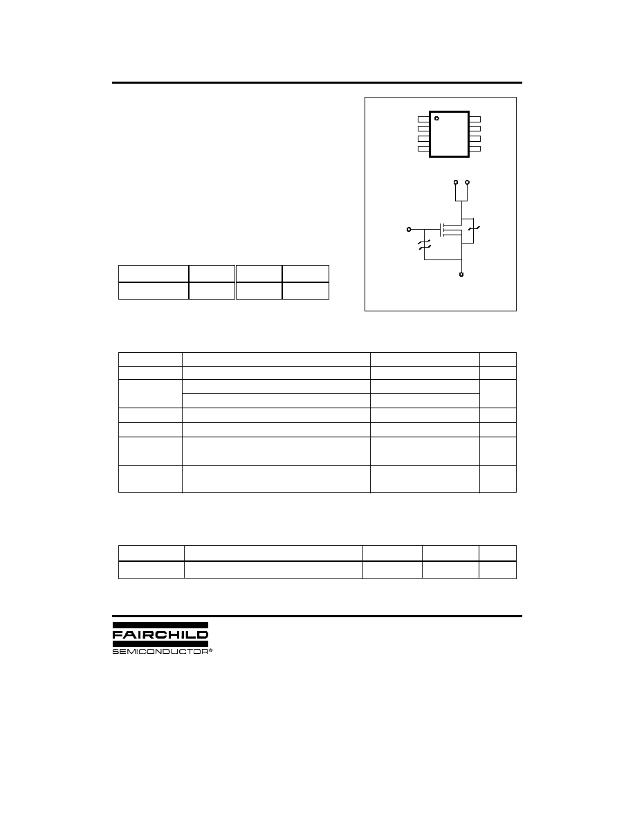
8 SOIC
S
1
G
1
S
2
G
2
D
1
D
1
D
2
D
2
4
3
1
2
5
6
8
7
Top View
N -Channel MOSFET
Dual N-CHANNEL POWER MOSFET
!
Lower R
DS(ON)
!
Improved Inductive Ruggedness
!
Fast Switching Times
!
Low Input Capacitance
!
Extended Safe Operating Area
!
Improved High Temperature Reliability
FEATURES
Absolute Maximum Ratings
Drain-to-Source Voltage
Continuous Drain Current T
A
=25
Continuous Drain Current T
A
=70
Drain Current-Pulsed
Gate-to-Source Voltage
Total Power Dissipation ( T
A
=25
)
( T
A
=70
)
Operating and Junction Storage
Temperature Range
Characteristic
Units
Symbol
I
D
P
D
A
V
A
V
DSS
V
W
Part Number
BV
DSS
R
DS(on)
I
D
SSD2009
50V
0.13
3.0A
Product Summary
V
GS
I
DM
T
J
, T
STG
Thermal Resistance
Junction-to-Ambient
R
JA
/W
Characteristic
Max.
Units
Symbol
Typ.
--
62.5
Value
Rev. A1
D
1
,D
2
G
1
,G
2
S
1
,S
2
D
1
,D
2
Dual N-CHANNEL
POWER MOSFET
Electrical Characteristics
(T
C
=25
unless otherwise specified)
Drain-Source Breakdown Voltage
Gate Threshold Voltage
Gate-Source Leakage , Forward
Gate-Source Leakage , Reverse
Characteristic
Symbol
Max. Units
Typ.
Min.
Test Condition
Static Drain-Source
On-State Resistance
Forward Transconductance
Turn-On Delay Time
Rise Time
Turn-Off Delay Time
Fall Time
Total Gate Charge
Gate-Source Charge
Gate-Drain ("Miller") Charge
g
fs
t
d(on)
t
r
t
d(off)
t
f
Q
g
Q
gs
Q
gd
BV
DSS
V
GS(th)
R
DS(on)
I
GSS
I
DSS
V
V
nA
nA
A
ns
nC
--
--
--
--
--
--
--
--
V
GS
=0V,I
D
=250
A
V
DS
= 5V ,I
D
=250
A
V
GS
=20V
V
GS
=-20V
V
DS
=40V
V
DS
=40V,T
C
=55
V
GS
=10V,I
D
=3.0A
V
GS
=4.5V,I
D
=1.5A
V
DS
=15V,I
D
=3.0A
V
DD
=25V,I
D
=1.0A,
R
0
=6.0
,
V
DS
=25V,V
GS
=10V,
I
D
=2.0A
Drain-to-Source Leakage Current
Source-Drain Diode Ratings and Characteristics
Continuous Source Current
(Body Diode)
Diode Forward Voltage
Reverse Recovery Time
I
S
Characteristic
Symbol
Max. Units
Typ.
Min.
Test Condition
--
--
--
A
V
ns
Modified MOSFET Symbol
Showing the Integral Reverse
P-N Junction Rectifier
I
DON
On-State Drain-Source Current
A
V
DS
=5V ,V
GS
=10V
V
SD
t
rr
T
A
=25
,I
S
=1.5A,V
GS
=0V
T
A
=25
,I
F
=1.5A,di
F
/dt=100A/
s
SSD2009A
50
1.0
--
--
--
--
10
--
--
--
--
--
--
--
--
--
0.065
0.084
--
3.0
100
-100
2.0
25
--
0.13
0.2
--
20
20
70
50
25
--
--
7.0
16
16
40
23
17
1.8
3.9
--
--
100
2.0
1.2
--
D
S
G
Notes ;
Repetitive Rating : Pulse Width Limited by Maximum Junction Temperature
Pulse Test : Pulse Width = 250
s, Duty Cycle
2%
Essentially Independent of Operating Temperature
S
Dual N-CHANNEL
POWER MOSFET
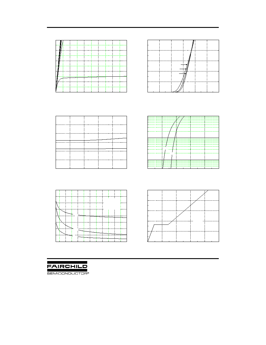
Fig 1. Output Characteristics
Fig 2. Transfer Characteristics
Fig 6. Gate Charge vs. Gate-Source Voltage
Fig 5. Capacitance vs. Drain-Source Voltage
Fig 3. On-Resistance vs. Drain Current
Fig 4. Source-Drain Forward Voltage
SSD2009A
0
2
4
6
8
10
0
2
4
6
8
10
Vgs= 3V
Vgs= 10,9,8,7,6,5,4V
I
D
, Dr
ai
n Cu
rr
en
t [A
]
V
DS
, Drain-Source Voltage [V]
0
1
2
3
4
5
6
0
2
4
6
8
10
150
o
C
25
o
C
-55
o
C
V
GS
, Gate-Source Voltage [V]
I
D
,
Dra
in C
urre
nt
[A]
5
10
15
20
25
30
0
200
400
600
800
@ Notes :
1. V
GS
= 0 V
2. f = 1 MHz
C
rss
C
oss
C
iss
Ca
pa
ci
ta
nc
e
[
p
F
]
V
DS
, Drain-Source Voltage [V]
0.0
0.4
0.8
1.2
1.6
2.0
10
-1
10
0
10
1
150
o
C
25
o
C
I
DR
, Re
ve
rs
e Dr
ai
n C
u
r
r
e
n
t
[A
]
V
SD
, Source-Drain Voltage [V]
0
4
8
12
16
20
0
2
4
6
8
10
V
DS
= 25 V
I
D
= 2.0A
V
GS
, Ga
te
-S
ou
rc
e Vo
l
t
a
g
e
[V
]
Q
G
, Total Gate Charge [nC]
0
2
4
6
8
10
0.02
0.04
0.06
0.08
0.10
0.12
0.14
V
GS
=4.5 V
V
GS
= 10 V
R
DS
(o
n)
, [
]
Dr
ai
n-
So
ur
ce
O
n
-
Res
is
ta
nc
e
I
D
, Drain Current [A]
DISCLAIMER
FAIRCHILD SEMICONDUCTOR RESERVES THE RIGHT TO MAKE CHANGES WITHOUT FURTHER
NOTICE TO ANY PRODUCTS HEREIN TO IMPROVE RELIABILITY, FUNCTION OR DESIGN. FAIRCHILD
DOES NOT ASSUME ANY LIABILITY ARISING OUT OF THE APPLICATION OR USE OF ANY PRODUCT
OR CIRCUIT DESCRIBED HEREIN; NEITHER DOES IT CONVEY ANY LICENSE UNDER ITS PATENT
RIGHTS, NOR THE RIGHTS OF OTHERS.
TRADEMARKS
The following are registered and unregistered trademarks Fairchild Semiconductor owns or is authorized to use and is
not intended to be an exhaustive list of all such trademarks.
LIFE SUPPORT POLICY
FAIRCHILDS PRODUCTS ARE NOT AUTHORIZED FOR USE AS CRITICAL COMPONENTS IN LIFE SUPPORT
DEVICES OR SYSTEMS WITHOUT THE EXPRESS WRITTEN APPROVAL OF FAIRCHILD SEMICONDUCTOR CORPORATION.
As used herein:
1. Life support devices or systems are devices or
systems which, (a) are intended for surgical implant into
the body, or (b) support or sustain life, or (c) whose
failure to perform when properly used in accordance
with instructions for use provided in the labeling, can be
reasonably expected to result in significant injury to the
user.
2. A critical component is any component of a life
support device or system whose failure to perform can
be reasonably expected to cause the failure of the life
support device or system, or to affect its safety or
effectiveness.
PRODUCT STATUS DEFINITIONS
Definition of Terms
Datasheet Identification
Product Status
Definition
Advance Information
Preliminary
No Identification Needed
Obsolete
This datasheet contains the design specifications for
product development. Specifications may change in
any manner without notice.
This datasheet contains preliminary data, and
supplementary data will be published at a later date.
Fairchild Semiconductor reserves the right to make
changes at any time without notice in order to improve
design.
This datasheet contains final specifications. Fairchild
Semiconductor reserves the right to make changes at
any time without notice in order to improve design.
This datasheet contains specifications on a product
that has been discontinued by Fairchild semiconductor.
The datasheet is printed for reference information only.
Formative or
In Design
First Production
Full Production
Not In Production
MICROWIRE
OPTOLOGIC
OPTOPLANAR
PACMAN
POP
Power247
PowerTrench
QFET
QS
QT Optoelectronics
Quiet Series
FAST
FASTr
FRFET
GlobalOptoisolator
GTO
HiSeC
I
2
C
ISOPLANAR
LittleFET
MicroFET
MicroPak
Rev. H5
â
ACEx
Bottomless
CoolFET
CROSSVOLT
DenseTrench
DOME
EcoSPARK
E
2
CMOS
TM
EnSigna
TM
FACT
FACT Quiet Series
SILENT SWITCHER
SMART START
SPM
STAR*POWER
Stealth
SuperSOT-3
SuperSOT-6
SuperSOT-8
SyncFET
TinyLogic
TruTranslation
â
â
â
STAR*POWER is used under license
UHC
UltraFET
VCX
â