 | ÐлекÑÑоннÑй компоненÑ: X9408Y | СкаÑаÑÑ:  PDF PDF  ZIP ZIP |
X9408_1.2.9.fm
REV 1.2.9 1/30/03
Characteristics subject to change without notice.
1 of 22
www.xicor.com
Low Noise/Low Power/2-Wire Bus
X9408
Quad Digitally Controlled (XDCP
TM
) Potentiometers
FEATURES
· Four potentiometers in one package
· 64 resistor taps per potentiometer
· 2-wire serial interface
· Wiper resistance, 40
typical at 5V
· Four nonvolatile data registers for each pot
· Nonvolatile storage of wiper position
· Standby current < 1µA max (total package)
· V
CC
= 2.7V to 5.5V operation
V+ = 2.7V to 5.5V
V = 2.7V to 5.5V
· 10K
, 2.5K
end to end resistances
· High reliability
--Endurance100,000 data changes per bit per
register
--Register data retention100 years
· 24-lead SOIC, 24-lead TSSOP, and 24-lead CSP
(Chip Scale Package) packages
DESCRIPTION
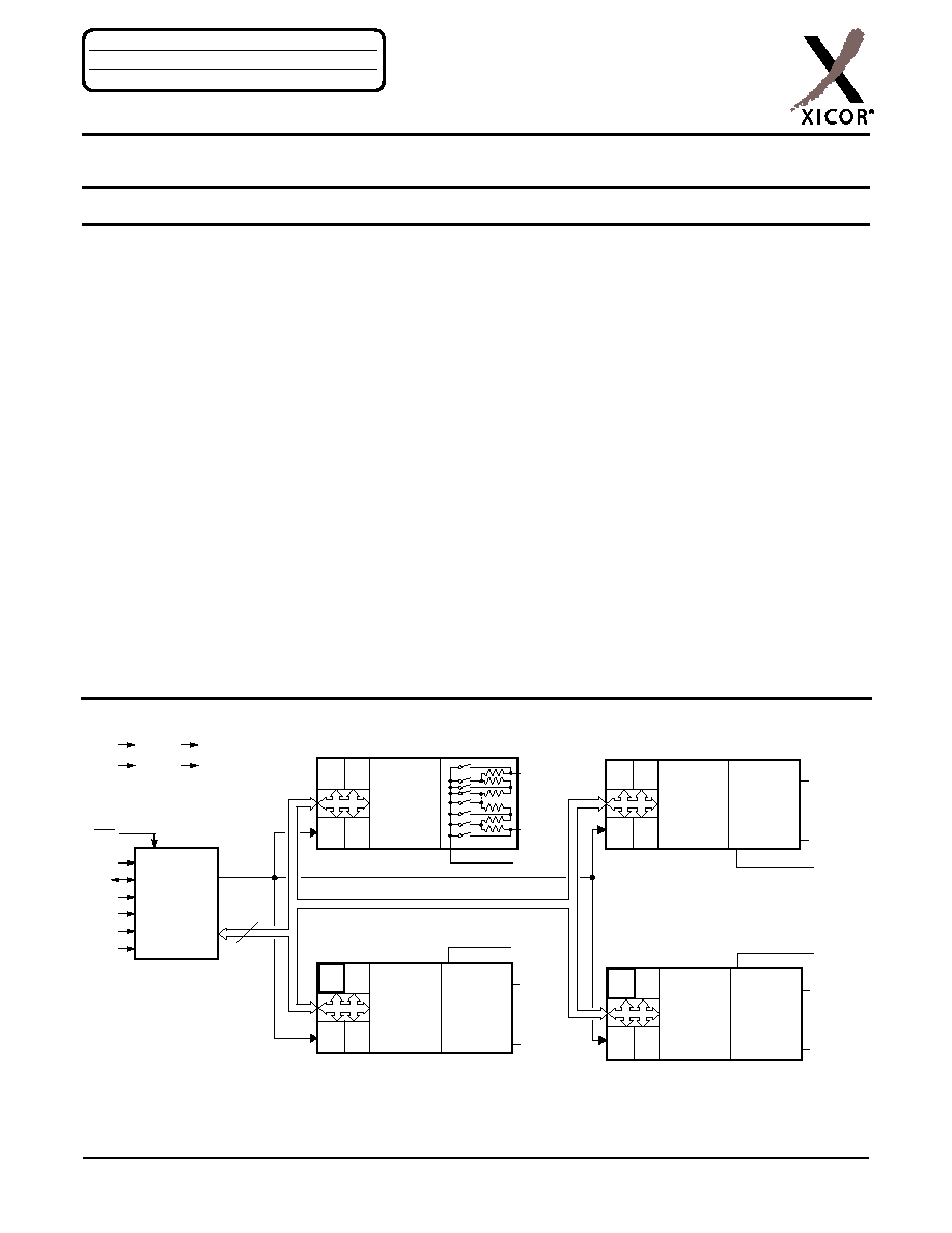
The X9408 integrates four digitally controlled
potentiometers (XDCP) on a monolithic CMOS
integrated circuit.
The digital controlled potentiometer is implemented
using 63 resistive elements in a series array. Between
each element are tap points connected to the wiper
terminal through switches. The position of the wiper on
the array is controlled by the user through the 2-wire
bus interface. Each potentiometer has associated with
it a volatile Wiper Counter Register (WCR) and four
non-volatile Data Registers that can be directly written
to and read by the user. The contents of the WCR
controls the position of the wiper on the resistor array
though the switches. Powerup recalls the contents of
the default data register (DR0) to the WCR.
The XDCP can be used as a three-terminal
potentiometer or as a two terminal variable resistor in
a wide variety of applications including control,
parameter adjustments, and signal processing.
BLOCK DIAGRAM
Interface
and
Control
Circuitry
SCL
SDA
A0
A1
A2
A3
R0 R1
R2 R3
Wiper
Counter
Register
(WCR)
Resistor
Array
Pot 1
V
H1
/R
H1
V
L1
/R
L1
R0 R1
R2 R3
Wiper
Counter
Register
(WCR)
V
H0
/R
H0
V
L0
/R
L0
Data
8
V
W0
/R
W0
V
W1
/R
W1
R0 R1
R2 R3
Resistor
Array
V
H2
/R
H2
V
L2
/R
L2
V
W2
/R
W2
R0 R1
R2 R3
Resistor
Array
V
H3
/R
H3
V
L3
/R
L3
V
W3
/R
W3
Wiper
Counter
Register
(WCR)
Wiper
Counter
Register
(WCR)
Pot 3
Pot 2
WP
Pot 0
V
CC
V
SS
V+
V-
A
PPLICATION
N
OTES
A V A I L A B L E
AN99 · AN115 · AN124 · AN133 · AN134 · AN135
X9408
Characteristics subject to change without notice.
2 of 22
REV 1.2.9 1/30/03
www.xicor.com
PIN DESCRIPTIONS
Host Interface Pins
Serial Clock (SCL)
The SCL input is used to clock data into and out of the
X9408.
Serial Data (SDA)
SDA is a bidirectional pin used to transfer data into
and out of the device. It is an open drain output and
may be wire-ORed with any number of open drain or
open collector outputs. An open drain output requires
the use of a pull-up resistor. For selecting typical
values, refer to the guidelines for calculating typical
values on the bus pull-up resistors graph.
Device Address (A
0
A
3
)
The address inputs are used to set the least significant
4 bits of the 8-bit slave address. A match in the slave
address serial data stream must be made with the
address input in order to initiate communication with
the X9408. A maximum of 16 devices may occupy the
2-wire serial bus.
Potentiometer Pins
V
H
/R
H
(V
H0
/R
H0
V
H3
/R
H3
), V
L
/R
L
(V
L0
/R
L0
V
L3
/R
L3
)
The V
H
/R
H
and V
L
/R
L
inputs are equivalent to the
terminal connections on either end of a mechanical
potentiometer.
V
W
/R
W
(V
W0
/R
W0
V
W3
/R
W3
)
The wiper outputs are equivalent to the wiper output of
a mechanical potentiometer.
Hardware Write Protect Input (WP)
The WP pin when low prevents nonvolatile writes to
the Data Registers.
Analog Supplies V+, V-
The Analog Supplies V+, V- are the supply voltages
for the XDCP analog section.
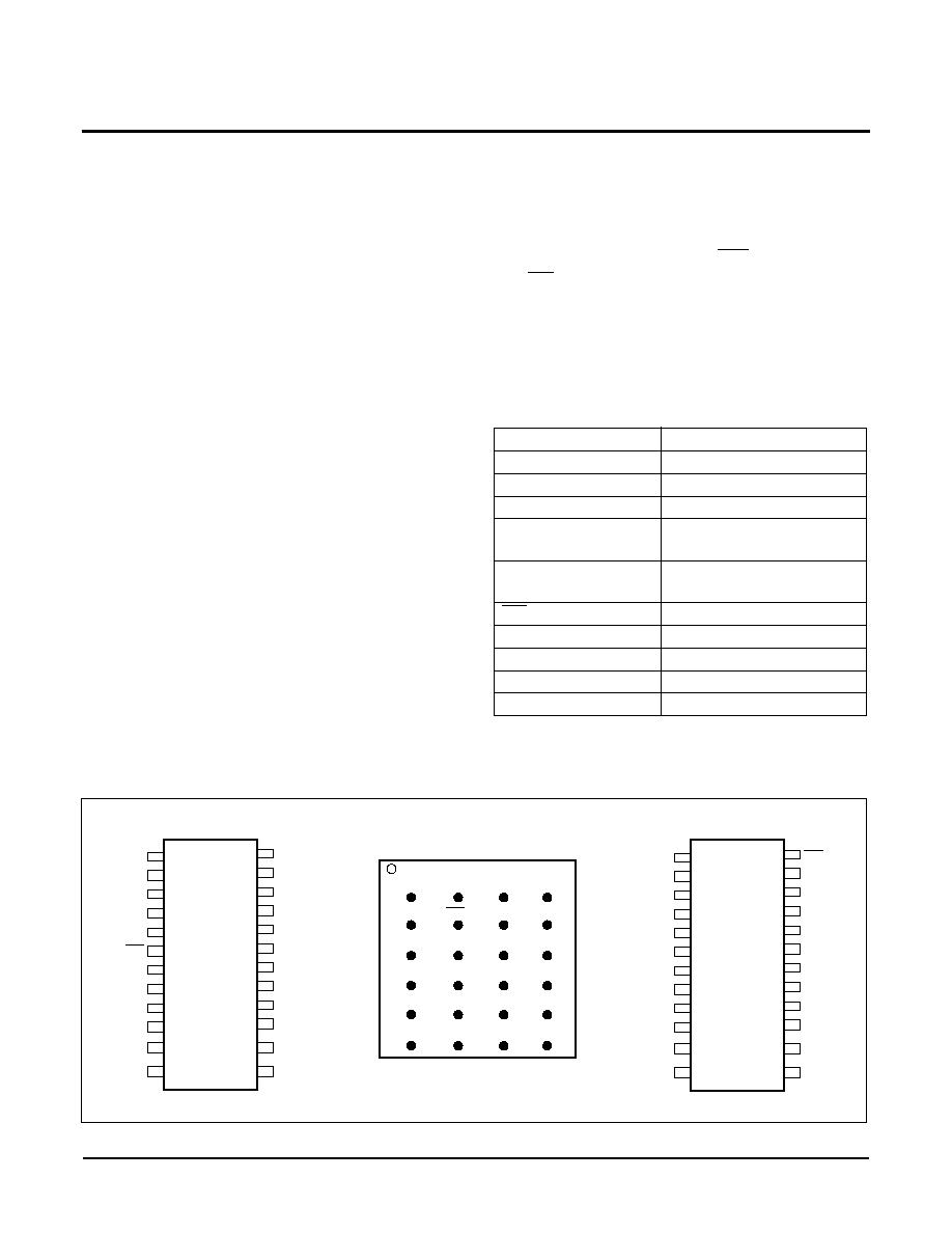
PIN NAMES
Symbol
Description
SCL
Serial Clock
SDA
Serial Data
A0-A3
Device Address
V
H0
/R
H0
V
H3
/R
H3
,
V
L0
/R
L0
V
L3
/R
L3
Potentiometer Pins
(terminal equivalent)
V
W0
/R
W0
V
W3
/R
W3
Potentiometer Pins
(wiper equivalent)
WP
Hardware Write Protection
V+,V-
Analog Supplies
V
CC
System Supply Voltage
V
SS
System Ground
NC
No Connection
PIN CONFIGURATION
V
CC
V
L0
/R
L0
V
H0
/R
H0
WP
SDA
A
1
1
2
3
4
5
6
7
8
9
10
24
23
22
21
20
19
18
17
16
15
V+
V
L3
/R
L3
V
H3
/R
H3
V
W3
/R
W3
A
0
NC
A
3
SCL
V
L2
/R
L2
V
H2
/R
H2
DIP/SOIC
X9408
V
SS
V
W0
/R
W0
14
13
11
12
A
2
V
L1
/R
L1
V
H1
/R
H1
V
W1
/R
W1
V
W2
/R
W2
V-
SDA
A
1
V
H2
/R
H2
1
2
3
4
5
6
7
8
9
10
24
23
22
21
20
19
18
17
16
15
WP
A
2
V
W0
/R
W0
V
CC
V+
V
L3
/R
L3
V
H3
/R
H3
V
W3
/R
W3
TSSOP
X9408
V
W2
/R
W2
14
13
11
12
A
3
V
L1
/R
L1
V
H1
/R
H1
V
W1
/R
W1
A
0
NC
V
H0
/R
H0
V-
SCL
V
L2
/R
L2
V
L0
/R
L0
V
SS
2
3
4
A
B
C
D
E
F
Top ViewBumps Down
R
W0
R
L0
V+
A 0
A
3
R
L1
V
CC
R
L3
R
W3
NC
SDA
R
W1
SCL
R
L2
WP
V-
R
H0
R
H1
R
H3
R
H2
V
SS
R
W2
A
2
A
1
1
CSP
X9408
Characteristics subject to change without notice.
3 of 22
REV 1.2.9 1/30/03
www.xicor.com
PRINCIPLES OF OPERATION
The X9408 is a highly integrated microcircuit
incorporating four resistor arrays and their associated
registers and counters and the serial interface logic
providing direct communication between the host and
the XDCP potentiometers.
Serial Interface
The X9408 supports a bidirectional bus oriented
protocol. The protocol defines any device that sends
data onto the bus as a transmitter and the receiving
device as the receiver. The device controlling the
transfer is a master and the device being controlled is
the slave. The master will always initiate data transfers
and provide the clock for both transmit and receive
operations. Therefore, the X9408 will be considered a
slave device in all applications.
Clock and Data Conventions
Data states on the SDA line can change only during
SCL LOW periods (t
LOW
). SDA state changes during
SCL HIGH are reserved for indicating start and stop
conditions.
Start Condition
All commands to the X9408 are preceded by the start
condition, which is a HIGH to LOW transition of SDA
while SCL is HIGH (t
HIGH
). The X9408 continuously
monitors the SDA and SCL lines for the start condition
and will not respond to any command until this
condition is met.
Stop Condition
All communications must be terminated by a stop
condition, which is a LOW to HIGH transition of SDA
while SCL is HIGH.
Acknowledge
Acknowledge is a software convention used to provide
a positive handshake between the master and slave
devices on the bus to indicate the successful receipt of
data. The transmitting device, either the master or the
slave, will release the SDA bus after transmitting eight
bits. The master generates a ninth clock cycle and
during this period the receiver pulls the SDA line LOW
to acknowledge that it successfully received the eight
bits of data.
The X9408 will respond with an acknowledge after
recognition of a start condition and its slave address
and once again after successful receipt of the
command byte. If the command is followed by a data
byte the X9408 will respond with a final acknowledge.
Array Description
The X9408 is comprised of four resistor arrays. Each
array contains 63 discrete resistive segments that are
connected in series. The physical ends of each array
are equivalent to the fixed terminals of a mechanical
potentiometer (R
H
and R
L
inputs).
At both ends of each array and between each resistor
segment is a CMOS switch connected to the wiper
(R
W
) output. Within each individual array only one
switch may be turned on at a time. These switches are
controlled by the Wiper Counter Register (WCR). The
six bits of the WCR are decoded to select, and enable,
one of sixty-four switches.
The WCR may be written directly, or it can be changed
by transferring the contents of one of four associated
Data Registers into the WCR. These Data Registers
and the WCR can be read and written by the host
system.
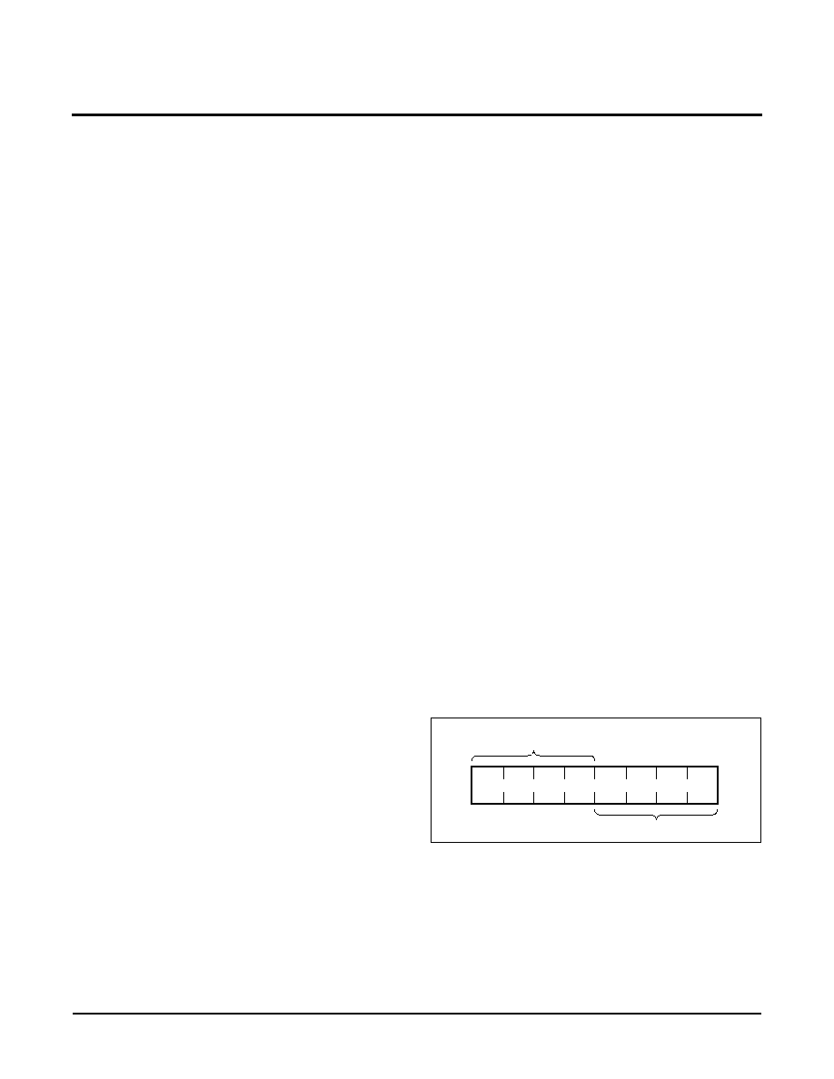
Device Addressing
Following a start condition the master must output the
address of the slave it is accessing. The most
significant four bits of the slave address are the device
type identifier (refer to Figure 1 below). For the X9408
this is fixed as 0101[B].
Figure 1. Slave Address
The next four bits of the slave address are the device
address. The physical device address is defined by the
state of the A
0
-A
3
inputs. The X9408 compares the
serial data stream with the address input state; a
successful compare of all four address bits is required
for the X9408 to respond with an acknowledge. The
A
0
A
3
inputs can be actively driven by CMOS input
signals or tied to V
CC
or V
SS
.
1
0
0
A3
A2
A1
A0
Device Type
Identifier
Device Address
1
X9408
Characteristics subject to change without notice.
4 of 22
REV 1.2.9 1/30/03
www.xicor.com
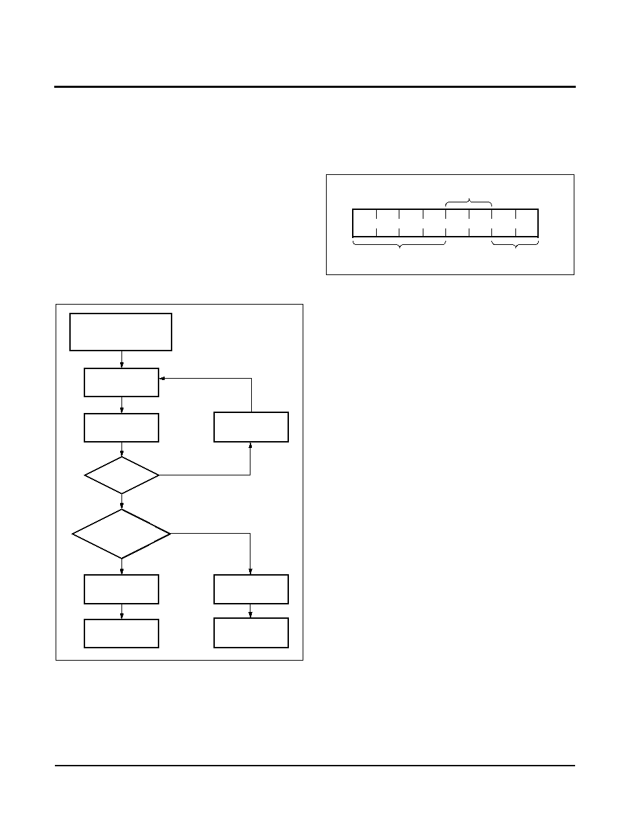
Acknowledge Polling
The disabling of the inputs, during the internal
Nonvolatile write operation, can be used to take
advantage of the typical 5ms EEPROM write cycle
time. Once the stop condition is issued to indicate the
end of the nonvolatile write command the X9408
initiates the internal write cycle. ACK polling can be
initiated immediately. This involves issuing the start
condition followed by the device slave address. If the
X9408 is still busy with the write operation no ACK will
be returned. If the X9408 has completed the write
operation an ACK will be returned and the master can
then proceed with the next operation.
Flow 1. ACK Polling Sequence
Instruction Structure
The next byte sent to the X9408 contains the instruction
and register pointer information. The four most
significant bits are the instruction. The next four bits
point to one of the two pots and when applicable they
point to one of four associated registers. The format is
shown below in Figure 2.
Figure 2. Instruction Byte Format
The four high order bits define the instruction. The next
two bits (R1 and R0) select one of the four registers
that is to be acted upon when a register oriented
instruction is issued. The last bits (P1, P0) select which
one of the four potentiometers is to be affected by the
instruction.
Four of the nine instructions end with the transmission
of the instruction byte. The basic sequence is
illustrated in Figure 3. These two-byte instructions
exchange data between the Wiper Counter Register
and one of the Data Registers. A transfer from a Data
Register to a Wiper Counter Register is essentially a
write to a static RAM. The response of the wiper to this
action will be delayed t
WRL
. A transfer from the Wiper
Counter Register (current wiper position), to a data
register is a write to nonvolatile memory and takes a
minimum of t
WR
to complete. The transfer can occur
between one of the four potentiometers and one of its
associated registers; or it may occur globally, wherein
the transfer occurs between all of the potentiometers
and one of their associated registers.
Four instructions require a three-byte sequence to
complete. These instructions transfer data between the
host and the X9408; either between the host and one
of the data registers or directly between the host and
the Wiper Counter Register. These instructions are:
Read Wiper Counter Register (read the current wiper
position of the selected pot), Write Wiper Counter
Register (change current wiper position of the selected
pot), Read Data Register (read the contents of the
selected nonvolatile register) and Write Data Register
(write a new value to the selected Data Register). The
sequence of operations is shown in Figure 4.
Nonvolatile Write
Command Completed
Enter ACK Polling
Issue
START
Issue Slave
Address
ACK
Returned?
Further
Operation?
Issue
Instruction
Issue STOP
NO
YES
YES
Proceed
Issue STOP
NO
Proceed
I1
I2
I3
I0
R1
R0
P1
P0
Wiper Counter
Register
Select
Instructions
Register Select
X9408
Characteristics subject to change without notice.
5 of 22
REV 1.2.9 1/30/03
www.xicor.com
Figure 3. Two-Byte Instruction Sequence
S
T
A
R
T
0
1
0
1
A3
A2
A1
A0
A
C
K
I3
I2
I1
I0
R1
R0
P1 P0
A
C
K
SCL
SDA
S
T
O
P
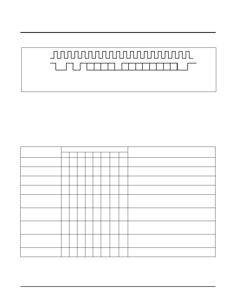
The Increment/Decrement command is different from
the other commands. Once the command is issued and
the X9408 has responded with an acknowledge, the
master can clock the selected wiper up and/or down in
one segment steps; thereby, providing a fine tuning
capability to the host. For each SCL clock pulse (t
HIGH
)
while SDA is HIGH, the selected wiper will move one
resistor segment towards the R
H
terminal. Similarly, for
each SCL clock pulse while SDA is LOW, the selected
wiper will move one resistor segment towards the R
L
terminal. A detailed illustration of the sequence and
timing for this operation are shown in Figures 5 and 6
respectively.
Table 1. Instruction Set
Note:
(7) 1/0 = data is one or zero
Instruction
Instruction Set
Operation
I
3
I
2
I
1
I
0
R
1
R
0
P
1
P
0
Read Wiper Counter
Register
1
0
0
1
0
0
P
1
P
0
Read the contents of the Wiper Counter Register
pointed to by P
1
P
0
Write Wiper Counter
Register
1
0
1
0
0
0
P
1
P
0
Write new value to the Wiper Counter Register pointed
to by P
1
P
0
Read Data Register
1
0
1
1
R
1
R
0
P
1
P
0
Read the contents of the Data Register pointed to by
P
1
P
0
and R
1
R
0
Write Data Register
1
1
0
0
R
1
R
0
P
1
P
0
Write new value to the Data Register pointed to by
P
1
P
0
and R
1
R
0
XFR Data Register to
Wiper Counter Register
1
1
0
1
R
1
R
0
P
1
P
0
Transfer the contents of the Data Register pointed to
by P
1
P
0
and R
1
R
0
to its associated Wiper Counter
Register
XFR Wiper Counter
Register to Data
Register
1
1
1
0
R
1
R
0
P
1
P
0
Transfer the contents of the Wiper Counter Register
pointed to by P
1
P
0
to the Data Register pointed to
by R
1
R
0
Global XFR Data Reg-
isters to Wiper Counter
Registers
0
0
0
1
R
1
R
0
0
0
Transfer the contents of the Data Registers pointed to
by R
1
R
0
of all four pots to their respective Wiper
Counter Registers
Global XFR Wiper
Counter Registers to
Data Register
1
0
0
0
R
1
R
0
0
0
Transfer the contents of both Wiper Counter Regis-
ters to their respective Data Registers pointed to by
R
1
R
0
of all four pots
Increment/Decrement
Wiper Counter Register
0
0
1
0
0
0
P
1
P
0
Enable Increment/decrement of the Wiper Counter
Register pointed to by P
1
P
0