DC≠20 GH
Z
MMIC SPST N
ON
-R
EFLECTIVE
S
WITCH
Specifications subject to change without notice
Filtronic Compound Semiconductors Ltd
Tel: +44 (0) 1325 301111
Fax: +44 (0) 1325 306177
Email:
sales@filcs.com
Website:
www.filtronic.com
1
Preliminary Datasheet v2.1
FMS2029
YPICAL
A
PPLICATIONS
:
s
(ECM, ESM)
F
EATURES
:
∑
Available in die form
∑
Both ports Non-Reflective
∑
Low Insertion loss 2.2dB at 20 GHz typical
∑
Very high isolation 50dB at 20 GHz typical
∑
Excellent low control voltage performance
G
ENERAL
D
ESCRIPTION
:
The FMS2029 is a loss, high isolation
broadband single pole single throw Gallium
Arsenide switch designed for use in broadband
communications, instrumentation and
electronic warfare applications. It offers non-
reflective properties from both ports. The die
is fabricated using the Filtronic FL05 0.5
µ
m
switch process technology that offers leading
edge performance optimised for switch
applications.
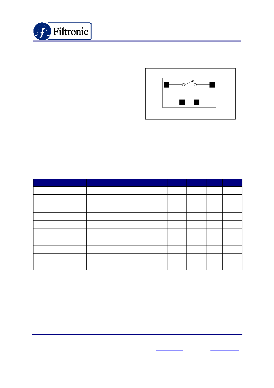
F
UNCTIONAL
S
CHEMATIC
:
RFin
RFout
V1
V2
RFin
RFout
V1
V2
RFin
RFout
V1
V2
T
∑
Broadband communication
∑
Instrumentation
∑
Electronic warfare
E
LECTRICAL
S
PECIFICATIONS
(based on on-wafer measurements):
P
ARAMETER
C
ONDITIONS
M
IN
T
YP
M
AX
U
NITS
Insertion Loss
(DC-10) GHz, Small Signal
1.4
dB
Insertion Loss
(10-15) GHz, Small Signal
1.6
dB
Insertion Loss
(15-20) GHz, Small Signal
2.2
dB
Isolation
(DC-10) GHz, Small Signal
70
dB
Isolation
(10-15) GHz, Small Signal
57
dB
Isolation
(15-20) GHz, Small Signal
50
dB
Input Return Loss (on state)
(DC-20) GHz, Small Signal
20
dB
Output Return Loss (on state)
(DC-20) GHz, Small Signal
20
dB
Output Return Loss (off state)
(DC-20) GHz, Small Signal
12
ns
P1dB
-5V control
26
dBm
Note: T
AMBIENT
= 25∞C, Vctrl = 0V/-5V, Z
IN
= Z
OUT
= 50

Specifications subject to change without notice
Filtronic Compound Semiconductors Ltd
Tel: +44 (0) 1325 301111
Fax: +44 (0) 1325 306177
Email:
sales@filcs.com
Website:
www.filtronic.com
2
Preliminary Datasheet v2.1
FMS2029
A
BSOLUTE
M
AXIMUM
R
ATINGS
:
Note: Exceeding any one of these absolute
maximum ratings may cause permanent
damage to the device.
P
AD
L
AYOUT
:
T
RUTH
T
ABLE
:
Note: -5V
±
0.2V; 0V
±
0.2V
Note: Co-ordinates are referenced from the bottom
left hand corner of the die to the centre of bond pad
opening
P
ARAMETER
S
YMBOL
A
BSOLUTE
M
AXIMUM
Max Input Power
Pin
+38dBm
Operating Temp
Toper
-40∞C to +100∞C
Storage Temp
Tstor
-55∞C to +150∞C
P
AD
N
AME
D
ESCRIPTION
P
IN
C
OORDINATES
(µm)
RFIN
RFIN
141,587
RFO
RFOUT
1789,587
V1
V1
901,161
V2
V2
1101,161
C
ONTROL
L
INE
RF P
ATH
V1
V2
RF
IN
-RF
O
-5V
0V
On (Low Loss)
0V
-5V
Off (Isolation)
RFI RFO
V1 V2
D
IE
S
IZE
(
µ
m)
D
IE
T
HICKNESS
(
µ
m)
M
IN
. B
OND
P
AD
P
ITCH
(
µ
m)
M
IN
. B
OND PAD
O
PENING
(
µ
m x
µ
m )
1910 x 1110
100
150
116 x 116

Specifications subject to change without notice
Filtronic Compound Semiconductors Ltd
Tel: +44 (0) 1325 301111
Fax: +44 (0) 1325 306177
Email:
sales@filcs.com
Website:
www.filtronic.com
3
Preliminary Datasheet v2.1
FMS2029
T
YPICAL
M
EASURED
P
ERFORMANCE
O
N
W
AFER
:
Note: Measurement Conditions V
CTRL
= -5V (low) & 0V (high), T
AMBIENT
= 25∞C unless otherwise stated
1
6
11
16
20
Frequency (GHz)
Insertion Loss (dB)
-3
-2.5
-2
-1.5
-1
-0.5
1
6
11
16
20
Frequency (GHz)
Isolation (dB)
-90
-80
-70
-60
-50
-40
-30
-20
-10
0
1
6
11
16
20
Frequency (GHz)
Input Return Loss (dB)
-40
-30
-20
-10
0
ON-STATE
OFF-STATE
1
6
11
16
20
Frequency (GHz)
Output Return Loss (dB)
-40
-30
-20
-10
0
ON-STATE
OFF-STATE

Specifications subject to change without notice
Filtronic Compound Semiconductors Ltd
Tel: +44 (0) 1325 301111
Fax: +44 (0) 1325 306177
Email:
sales@filcs.com
Website:
www.filtronic.com
4
Preliminary Datasheet v2.1
FMS2029
P
REFERRED
A
SSEMBLY
I
NSTRUCTIONS
:
GaAs devices are fragile and should be
handled with great care. Specially designed
collets should be used where possible.
The back of the die is metallised and the
recommended mounting method is by the use
of solder or conductive epoxy. If epoxy is
selected then it should be applied to the
attachment surface uniformly and sparingly to
avoid encroachment of epoxy on to the top
face of the die and ideally should not exceed
half the chip height. For automated dispense
Ablestick LMISR4 is recommended and for
manual dispense Ablestick 84-1 LMI or 84-1
LMIT are recommended. These should be
cured at a temperature of 150
∞
C for 1 hour in
an oven especially set aside for epoxy curing
only. If possible the curing oven should be
flushed with dry nitrogen.
This part has gold (Au) bond pads requiring
the use of gold (99.99% pure) bondwire. It is
recommended that 25.4
µ
m diameter gold wire
be used. Thermosonic ball bonding is
preferred. A nominal stage temperature of
150
∞
C and a bonding force of 40g has been
shown to give effective results for 25
µ
m wire.
Ultrasonic energy shall be kept to a minimum.
For this bonding technique, stage temperature
should not be raised above 200∞C and bond
force should not be raised above 60g.
Thermosonic wedge bonding and
thermocompression wedge bonding can also
be used to achieve good wire bonds.
Bonds should be made from the die first and
then to the mounting substrate or package.
The physical length of the bondwires should be
minimised especially when making RF or
ground connections.
H
ANDLING
P
RECAUTIONS
:
To avoid damage to the devices care should
be exercised during handling. Proper
Electrostatic Discharge (ESD) precautions
should be observed at all stages of storage,
handling, assembly, and testing. These
devices should be treated as Class 1A (0-500
V) as defined in JEDEC Standard No. 22-
A114. Further information on ESD control
measures can be found in MIL-STD-1686 and
MIL-HDBK-263.
A
PPLICATION
N
OTES
& D
ESIGN
D
ATA
:
Application Notes and design data including S-
parameters are available; please contact
Filtronic Compound Semiconductors Ltd.
D
ISCLAIMERS
:
This product is not designed for use in any
space based or life sustaining/supporting
equipment.
O
RDERING
I
NFORMATION
:
P
ART
N
UMBER
D
ESCRIPTION
FMS2029-000
Die in Waffle-pack
(Gel-pak available on request)