Preliminary Data Sheet
FPDA200V
H
IGH
P
ERFORMANCE
PHEMT
WITH
S
OURCE
V
IAS
Phone: (408) 988-1845
http:// www.filss.com
Revised: 2/25/02
Fax: (408) 970-9950
Email: sales@filss.com
∑
FEATURES
21 dBm Output Power at 1-dB
Compression at 18 GHz
12.5 dB Power Gain at 18 GHz
55% Power-Added Efficiency
Source Vias to Backside Metallization
∑
DESCRIPTION AND APPLICATIONS
The FPDA200V is an Aluminum Gallium Arsenide / Indium Gallium Arsenide (AlGaAs/InGaAs)
Pseudomorphic High Electron Mobility Transistor (PHEMT), utilizing an Electron-Beam direct-
write 0.25
µ
m by 200
µ
m Schottky barrier gate. The recessed "mushroom" gate structure minimizes
parasitic gate-source and gate resistances. The epitaxial structure and processing have been
optimized for high dynamic range.
Typical applications include high dynamic range driver stages for commercial applications including
wireless infrastructure systems, broad bandwidth amplifiers, and optical systems.
Source vias have been added for improved performance and assembly convenience. Each via hole
has 0.02 nH of inductance. Additionally, the via holes remove the need for source bond wires,
meaning only two bond wires are required for assembly. Because the via connects the source pad to
the backside metallization, self-bias configurations should be designed with caution.
∑
ELECTRICAL SPECIFICATIONS @ T
Ambient
= 25∞C
Parameter
Symbol
Test Conditions
Min
Typ
Max
Units
Saturated Drain-Source Current
I
DSS
V
DS
= 2 V; V
GS
= 0 V
40
60
85
mA
Power at 1-dB Compression
P-1dB
V
DS
= 5 V; I
DS
= 50% I
DSS
19
21
dBm
Power Gain at 1-dB Compression
G-1dB
V
DS
= 5 V; I
DS
= 50% I
DSS
11
12.5
dB
Power-Added Efficiency
PAE
V
DS
= 5 V; I
DS
= 50% I
DSS
55
%
Maximum Drain-Source Current
I
MAX
V
DS
= 2 V; V
GS
= 1 V
125
mA
Transconductance
G
M
V
DS
= 2 V; V
GS
= 0 V
50
70
mS
Gate-Source Leakage Current
I
GSO
V
GS
= -5 V
1
10
µ
A
Pinch-Off Voltage
V
P
V
DS
= 2 V; I
DS
= 1 mA
-0.25
-0.8
-1.5
V
Gate-Source Breakdown
Voltage Magnitude
|V
BDGS
|
I
GS
= 1 mA
6
7
V
Gate-Drain Breakdown
Voltage Magnitude
|V
BDGD
|
I
GD
= 1 mA
8
9
V
Thermal Resistivity
JC
260
∞
C/W
frequency=18 GHz
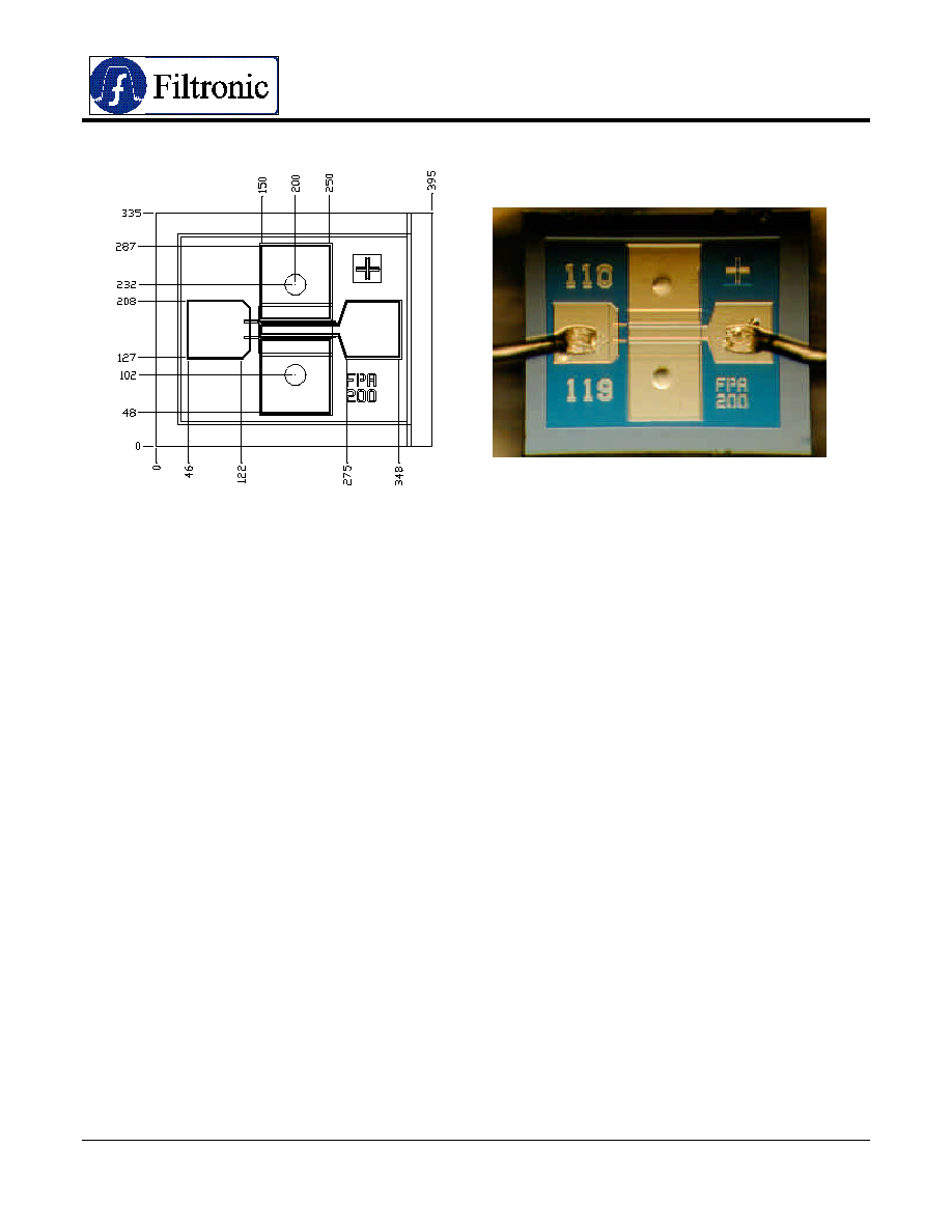
DRAIN
BOND
PAD
DIE SIZE: 15.6X13.2 mils (395x335
µ
m)
DIE THICKNESS: 3.9 mils (100
µ
m)
BONDING PADS: 3.1X3.1 mils (80x80
µ
m)
GATE
BOND
PAD

Preliminary Data Sheet
FPDA200V
H
IGH
P
ERFORMANCE
PHEMT
WITH
S
OURCE
V
IAS
Phone: (408) 988-1845
http:// www.filss.com
Revised: 2/25/02
Fax: (408) 970-9950
Email: sales@filss.com
∑
ABSOLUTE MAXIMUM RATINGS
Parameter
Symbol
Test Conditions
Min
Max
Units
Drain-Source Voltage
V
DS
T
Ambient
= 22
±
3
∞
C
8
V
Gate-Source Voltage
V
GS
T
Ambient
= 22
±
3
∞
C
-3
V
Drain-Source Current
I
DS
T
Ambient
= 22
±
3
∞
C
2xI
DSS
mA
Gate Current
I
G
T
Ambient
= 22
±
3
∞
C
10
mA
RF Input Power
P
IN
T
Ambient
= 22
±
3
∞
C
100
mW
Channel Operating Temperature
T
CH
T
Ambient
= 22
±
3
∞
C
175
∫C
Storage Temperature
T
STG
--
-65
175
∫C
Total Power Dissipation
P
TOT
T
Ambient
= 22
±
3
∞
C
550
mW
Notes:
∑
Operating conditions that exceed the Absolute Maximum Ratings could result in permanent damage to the device.
∑
Power Dissipation defined as: P
TOT
(P
DC
+ P
IN
) ≠ P
OUT
, where
P
DC
: DC Bias Power
P
IN
: RF Input Power
P
OUT
: RF Output Power
∑
Absolute Maximum Power Dissipation to be de-rated as follows above 25
∞
C:
P
TOT
= 550mW ≠ (3.7mW/
∞
C) x T
HS
where T
HS
= heatsink or ambient temperature.
∑
HANDLING PRECAUTIONS
To avoid damage to the devices care should be exercised during handling. Proper Electrostatic
Discharge (ESD) precautions should be observed at all stages of storage, handling, assembly, and
testing. These devices should be treated as Class 1A (0-500 V). Further information on ESD control
measures can be found in MIL-STD-1686 and MIL-HDBK-263.
∑
ASSEMBLY INSTRUCTIONS
The recommended die attach is gold/tin eutectic solder under a nitrogen atmosphere. Stage
temperature should be 280-290
∞
C; maximum time at temperature is one minute. The recommended
wire bond method is thermo-compression wedge bonding with 0.7 or 1.0 mil (0.018 or 0.025 mm)
gold wire. Stage temperature should be 250-260
∞
C.
∑
APPLICATIONS NOTES & DESIGN DATA
Applications Notes are available from your local Filtronic Sales Representative or directly from the
factory. Complete design data, including S-parameters, noise data, and large-signal models are
available on the Filtronic web site.