1
Item
Symbol
Rating
Unit
Drain-source voltage
V
DS
800
Continuous drain current
I
D
4
Pulsed drain current
I
D(puls]
10
Continuous reverse drain current
I
DR
4
Gate-source peak voltage
V
GS
�30
Max. power dissipation
P
D
60
Operating and storage
T
ch
+150
temperature range
T
stg
2SK1552-01L,S
FUJI POWER MOSFET
N-CHANNEL SILICON POWER MOSFET
Equivalent circuit schematic
Maximum ratings and characteristics
Absolute maximum ratings ( Tc=25�C unless otherwise specified)
Gate(G)
Source(S)
Drain(D)
V
A
A
A
V
W
�C
�C
-55 to +150
Outline Drawings
F- II SERIES
Features
High current
Low on-resistance
No secondary breakdown
Low driving power
High voltage
V
GS
=�30V Guarantee
Applications
Switching regulators
UPS
DC-DC converters
General purpose power amplifier
Electrical characteristics (T
c
=25�C unless otherwise specified)
Thermal characteristics
Item
Symbol
Test Conditions
Zero gate voltage drain current I
DSS
Min. Typ. Max. Units
V
V
�A
mA
nA
S
pF
ns
V
ns
Min. Typ. Max. Units
Thermal resistance
R
th(ch-a)
channel to ambient
R
th(ch-c)
channel to case
125
2.08
�C/W
�C/W
Symbol
V
(BR)DSS
V
GS(th)
I
GSS
R
DS(on)
g
fs
C
iss
C
oss
C
rss
t
d(on)
t
r
t
d(off)
t
f
V
SD
t
rr
Item
Drain-source breakdown voltage
Gate threshold voltage
Gate-source leakage current
Drain-source on-state resistance
Forward transconductance
Input capacitance
Output capacitance
Reverse transfer capacitance
Turn-on time t
on
(t
on
=t
d(on)
+t
r
)
Turn-off time t
off
(t
off
=t
d(off)
+t
f
)
Diode forward on-voltage
Reverse recovery time
Test Conditions
I
D
=1mA V
GS
=0V
I
D
=1mA V
DS
=V
GS
V
DS
=800V V
GS
=0V T
ch
=25�C
T
ch
=125�C
V
GS
=�30V V
DS
=0V
I
D
=2A V
GS
=10V
I
D
=2A V
DS
=25V
V
DS
=25V
V
GS
=0V
f=1MHz
V
CC
=600V R
G
=25
I
D
=4A
V
GS
=10V
I
F
=2xI
DR
V
GS
=0V T
ch
=25�C
I
F
=I
DR
di/dt=100A/
�
s T
ch
=25�C
800
2.5
3.5
5.0
10
500
0.2
1.0
10
100
3.0
4.5
2.0
4.0
800
1200
80
120
30
45
30
45
65
100
110
165
60
90
0.92
1.38
700
EIAJ
�
0.5
�
0.3
�
0.3
�
0.2
�
0.2
+0.2
--0.1
4.5
1.32
2.7
5.08
1.2
10
0.4
0.8
0.9
9.3
1.5
3.0
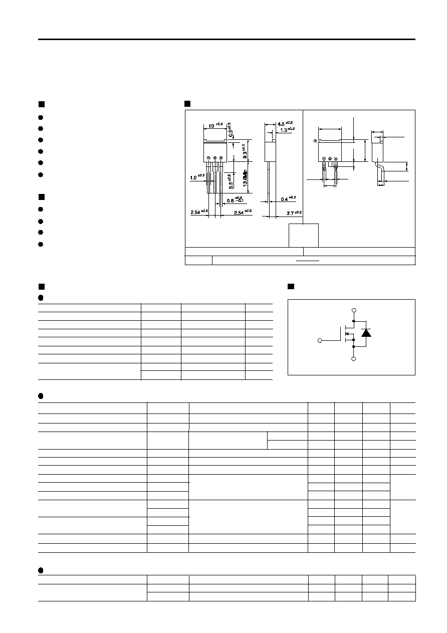
1. Gate
2, 4. Drain
3. Source
+0.5
+0.2
Max
L-type
S-type
1:Gate
2:Drain
3:Source

2
Characteristics
2SK1552-01L,S
FUJI POWER MOSFET
Typical output characteristics
V
DS
[ V ]
I
D
[ A ]
On state resistance vs. T
ch
R
DS(on)
[
]
T
ch
[ �C ]
Typical transfer characteristics
V
GS
[ V ]
I
D
[ A ]
Typical Drain-Source on state resistance vs. I
D
I
D
[ A ]
R
DS(on)
[ m
]
Typical forward transconductance vs. I
D
I
D
[ A ]
gfs
[ S ]
Gate threshold voltage vs. T
ch
T
ch
[ �C ]
V
GS(th)
[ V ]
0 10 20 30 40
6
4
2
0
8
6
4
2
0
15
10
5
0
-50 0 50 100 150
0 2 4 6 8 10 12
15
10
5
0
0 2 4 6 8 10
0 2 4 6 8
0 50 100 150
8
6
4
2
0
6.0
4.0
2.0
0

3
FUJI POWER MOSFET
Typical capacitance vs. V
DS
V
DS
[ V ]
C
[nF]
Typical input charge
V
DS
[ V ]
Qg
[ nC ]
Forward characteristics of reverse diode
0 0.4 0.8 1.2
V
SD
[ V ]
I
F
[ A ]
Allowable power dissipation vs. T
c
0 50 100 150
T
c
[ �C ]
P
D
[ W ]
Transient thermal impedance
t
[ sec. ]
R
th
[�C/W]
Safe operating area
I
D
[ A ]
V
DS
[ V ]
20
15
10
5
0
V
GS
[ V ]
10
5
1
0.5
0.1
2SK1552-01L,S
1.0
0.5
0.1
0.05
0.01
0 10 20 30
1000
800
600
400
200
0
0 20 40 60
60
40
20
0
10
0
10
-1
10
-2
10
-5
10
-4
10
-3
10
-2
10
-1
10
0
10
1
5 10 50 100 500 1000
10
5
1
0.5
0.1
0.05