
6MBI50UA-120
1200V / 50A 6 in one-package
Features
∑ High speed switching
∑ Voltage drive
∑ Low inductance module structure
Applications
∑ Inverter for Motor drive
∑ AC and DC Servo drive amplifier
Maximum ratings and characteristics
Absolute maximum ratings (at Tc=25∞C unless otherwise specified)
Item
Zero gate voltage collector current
Gate-Emitter leakage current
Gate-Emitter threshold voltage
Collector-Emitter saturation voltage
Input capacitance
Turn-on time
Turn-off time
Forward on voltage
Reverse recovery time
Lead resistance, terminal-chip*4
Resistance
B value
I
CES
I
GES
V
GE(th)
V
CE(sat)
(terminal)
V
CE(sat)
(chip)
C
ies
t
on
t
r
t
r(i)
t
off
t
f
V
F
(terminal)
V
F
(chip)
t
rr
R lead
R
B
≠
≠
1.0
≠
≠
200
4.5
6.5
8.5
≠
2.00
2.35
≠
2.25
≠
≠
1.75
2.10
≠
2.00
≠
≠
6
≠
≠
0.36
1.20
≠
0.21
0.60
≠
0.03
≠
≠
0.37
1.00
≠
0.07
0.30
≠
1.85
2.15
≠
1.95
≠
≠
1.60
1.90
≠
1.70
≠
≠
≠
0.35
≠
4.1
≠
≠
5000
≠
465
495
520
3305
3375
3450
V
GE
=0V, V
CE
=1200V
V
CE
=0V, V
GE
=±20V
V
CE
=20V, I
C
=50mA
V
GE
=15V, I
C
=50A
V
CE
=10V, V
GE
=0V, f=1MHz
V
CC
=600V
I
C
=50A
V
GE
=±15V
R
G
=22
V
GE
=0V
I
F
=50A
I
F
=50A
T=25∞C
T=100∞C
T=25/50∞C
mA
nA
V
V
nF
µs
V
µs
m
Electrical characteristics (at Tj=25∞C unless otherwise specified)
Thermal resistance characteristics
Thermal resistance
Contact Thermal resistance
≠
≠
0.45
≠
≠
0.73
≠
0.05
≠
IGBT
FWD
With thermal compound
∞C/W
∞C/W
∞C/W
*
1 :
All terminals should be connected together when isolation test will be done.
*
2 :
Two thermistor terminals should be connected together, each other terminals should be connected together and shorted
to base plate when isolation test will be done.
*
3
:Recommendable value : 2.5 to 3.5 N∑m(M5)
Symbols Conditions
Characteristics Unit
Min.
Typ.
Max.
Rth(j-c)
Rth(j-c)
Rth(c-f)*
5
IGBT Module U-Series
*
5
:
This is the value which is defined mounting on the additional cooling fin with thermal compound.
Tj=25∞C
Tj=125∞C
Tj=25∞C
Tj=125∞C
Tj=25∞C
Tj=125∞C
Tj=25∞C
Tj=125∞C
*
4
:Biggest internal terminal resistance among arm.
Items Symbols
Conditions
Characteristics Unit
Min.
Typ.
Max.
Item
Symbol
Collector-Emitter voltage
V
CES
Gate-Emitter voltaga
V
GES
Collector current
I
C
I
C
p
-I
C
-I
C
pulse
Collector Power Dissipation
P
C
Junction temperature
T
j
Storage temperature
T
stg
Isolation voltage
between terminal and copper base *1
V
iso
between thermistor and others *2
Screw Torque Mounting *3
-
Rating
1200
±20
75
50
150
100
50
100
275
+150
-40 to +125
2500
3.5
Unit
V
V
A
W
∞C
VAC
N∑m
Conditions
Continuous
1ms
1 device
AC:1min.
Tc=25∞C
Tc=80∞C
Tc=25∞C
Tc=80∞C
∑ Uninterruptible power supply
∑ Industrial machines, such as Welding machines
Inverter
Thermistor

IGBT Module
Characteristics (Representative)
6MBI50UA-120
Collector-Emitter voltage vs. Gate-Emitter voltage (typ.)
Collector current vs. Collector-Emitter voltage (typ.)
Tj= 125∞C / chip
Capacitance vs. Collector-Emitter voltage (typ.)
Dynamic Gate charge (typ.)
Collector current vs. Collector-Emitter voltage (typ.)
Tj= 25∞C / chip
Collector current vs. Collector-Emitter voltage (typ.)
VGE=15V / chip
Tj=25∞C / chip
VGE=0V, f= 1M Hz, Tj= 25∞C
Vcc=600V, Ic=50A, Tj= 25∞C
0
25
50
75
100
125
0
1
2
3
4
5
Collector current : Ic [A]
Collector-Emitter voltage : VCE [V]
VGE=20V
15V
12V
10V
8V
0
25
50
75
100
125
0
1
2
3
4
5
Collector current : Ic [A]
Collector-Emitter voltage : VCE [V]
VGE=20V
15V
12V
10V
8V
0
25
50
75
100
125
0
1
2
3
4
5
Collector current : Ic [A]
Collector-Emitter voltage : VCE [V]
Tj=125∞C
Tj=25∞C
0
2
4
6
8
10
5
10
15
20
25
Collector - Emitter voltage : VCE [ V ]
Gate - Emitter voltage : VGE [ V ]
Ic=100A
Ic=50A
Ic= 25A
0.1
1.0
10.0
100.0
0
10
20
30
Capacitance : Cies, Coes, Cres [ nF ]
Collector-Emitter voltage : VCE [V]
Cies
Coes
Cres
0
100
200
300
Collector-Emitter voltage : VCE [ 200V/div ]
Gate - Emitter voltage : VGE [ 5V/div ]
Gate charge : Qg [ nC ]
0
VGE
VCE

IGBT Module
6MBI50UA-120
Switching loss vs. Gate resistance (typ.)
+VGE=15V,-VGE <= 15V, RG >= 22 ,Tj <= 125∞C
Switching time vs. Collector current (typ.)
Vcc=600V, VGE=±15V, Rg=22, Tj= 25∞C
Vcc=600V, Ic=50A, VGE=±15V, Tj= 25∞C
Switching time vs. Collector current (typ.)
Vcc=600V, VGE=±15V, Rg=22, Tj=125∞C
Switching time vs. Gate resistance (typ.)
Switching loss vs. Collector current (typ.)
Vcc=600V, VGE=±15V, Rg=22
Vcc=600V, Ic=50A, VGE=±15V, Tj= 125∞C
Reverse bias safe operating area (max.)
10
100
1000
10000
0
25
50
75
100
Switching time : ton, tr, toff, tf [ nsec ]
ton
toff
tr
tf
10
100
1000
10000
0
25
50
75
100
Switching time : ton, tr, toff, tf [ nsec ]
toff
ton
tr
tf
10
100
1000
10000
10
100
1000
Switching time : ton, tr, toff, tf [ nsec ]
tr
tf
toff
ton
0
2
4
6
8
10
0
25
50
75
100
Switching loss : Eon, Eoff, Err [ mJ/pulse ]
Eon(125∞C)
Eon(25∞C)
Eoff(125∞C)
Err(125∞C)
Err(25∞C)
Eoff(25∞C)
0
10
20
30
40
50
10
100
1000
Switching loss : Eon, Eoff, Err [ mJ/pulse ]
Eoff
Err
Eon
0
25
50
75
100
125
0
400
800
1200
Collector current : Ic [ A ]

IGBT Module
6MBI50UA-120
Transient thermal resistance (max.)
Reverse recovery characteristics (typ.)
Vcc=600V, VGE=±15V, Rg=22
Forward current vs. Forward on voltage (typ.)
chip
Temperature characteristic (typ.)
0.1
1
10
100
-60 -40 -20
0
20 40 60 80 100 120 140 160 180
T emperature [∞C ]
Resistance : R [ k
]
0
25
50
75
100
125
0
1
2
3
4
Forward current : IF [ A ]
Forward on voltage : VF [ V ]
Tj=125∞C
Tj=25∞C
10
100
1000
0
25
50
75
100
Reverse recovery current : Irr [ A ]
Reverse recovery time : trr [ nsec ]
Forward current : IF [ A ]
trr (125∞C)
trr (25∞C)
Irr (125∞C)
Irr (25∞C)
0.01
0.10
1.00
0.001
0.010
0.100
1.000
Thermal resistanse : Rth(j-c) [ ∞C/W ]
Pulse width : Pw [ sec ]
FWD
IGBT
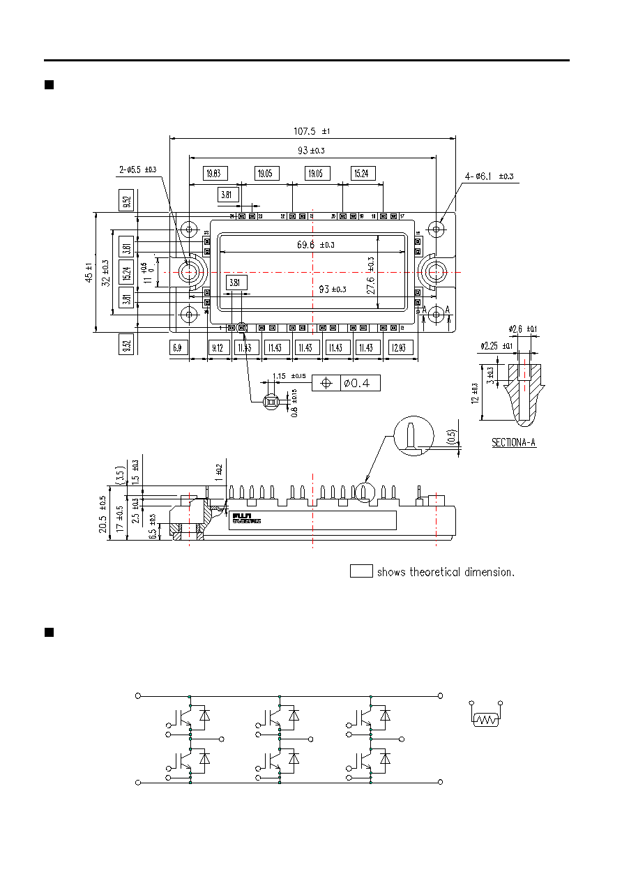
Outline Drawings, mm
M636
6MBI50UA-120
IGBT Module
Equivalent Circuit Schematic
( ) shows reference dimension.
U
V
W
1
2
3
4
5
6
7
8
9
10
11
12
13,14
15,16
19,20
21,22
17
18
23,24
25,26
27,28
U
V
W
1
2
3
4
5
6
7
8
9
10
11
12
13,14
15,16
19,20
21,22
17
18
23,24
25,26
27,28