 | –≠–ª–µ–∫—Ç—Ä–æ–Ω–Ω—ã–π –∫–æ–º–ø–æ–Ω–µ–Ω—Ç: E712545 | –°–∫–∞—á–∞—Ç—å:  PDF PDF  ZIP ZIP |

DS07-12545-1E
FUJITSU SEMICONDUCTOR
DATA SHEET
8-bit Proprietary Microcontroller
CMOS
F
2
MC-8L MB89960 Series
MB89965/P965A/F969A/
MB89PV960
s
s
s
s
DESCRIPTION
The MB89960 series is a single-chip microcontroller that utilizes the F
2
MC-8L core for low voltage and high speed
performance. The microcontroller contains a range of peripheral functions including timers, a serial interface, I
2
C
interface, A/D converter, and external interrupts. The internal I
2
C interface complies with the SM bus standard
and supports an SM bus battery controller.
s
s
s
s
FEATURES
∑ Range of package options
∑ QFP and MQFP packages (0.8 mm pitch)
∑ LQFP package (0.5 mm and 0.65 mm pitch)
∑ High speed operation at low voltage
Minimum instruction execution time
=
=
=
=
0.4
µ
s (for a 10 MHz oscillation)
∑ F
2
MC-8L CPU core
Instruction set optimized for controller applications
∑ Multiplication and division instructions
∑ 16-bit arithmetic operations
∑ Bit test branch instructions
∑ Bit manipulation instructions, etc.
∑ Dual-clock control system
∑ Main clock : 10 MHz max.
(Four speed settings available, oscillation halts in sub-clock mode)
∑ Sub-clock : 32.768 kHz (Operation clock for sub-clock mode)
∑ Four channels
∑ 8/16-bit timer/counter (8-bit
◊
2 channels or 16-bit
◊
1 channel)
∑ 21-bit timebase timer
∑ Clock prescaler (15-bit)
∑ Serial I/O
Selectable transfer format (MSB-first or LSB-first) supports communications with a wide range of devices.
∑ A/D converter
10-bit
◊
4 channels
MB89960 Series
2
∑ External interrupts
∑ External interrupt 1 (3 channels)
Three independent interrupt inputs can be used to recover from low-power consumption modes (with edge-
detection function)
∑ External interrupt 2 (1 channel with 8 inputs)
Eight inputs can be used to recover from low-power consumption modes (with "L" level detection function)
∑ Low-power consumption modes (standby modes)
∑ Stop mode (As all oscillations halt in sub-clock mode, current consumption falls to almost zero.)
∑ Sleep mode (The CPU stops to reduce the current consumption to approximately 1/3 of normal.)
∑ Clock mode (All operation halts other than the clock prescaler resulting in very low power consumption.)
∑ I
2
C interface*
∑ Supports Intel SM bus and Philips I
2
C bus standards.
∑ Uses a two-wire data transfer protocol.
∑ Max. 35 I/O ports
∑ Output-only ports (N-ch open drain)
: 6
∑ General-purpose I/O ports (CMOS) : 21
∑ Output-only ports (CMOS)
: 8
* : I
2
C license
The customer is licensed to use the Philips I
2
C patent when using this product in an I
2
C system that complies
with the Philips I
2
C standard specifications.
s
s
s
s
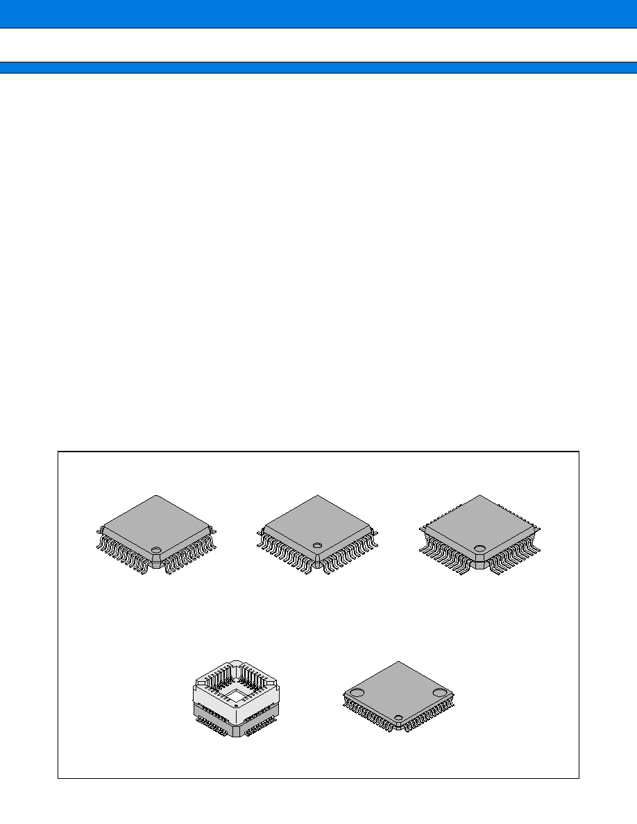
PACKAGE
Plastic LQFP, 48-pin
Plastic QFP, 48-pin
Plastic QFP, 48-pin
(FPT-48P-M05)
(FPT-48P-M13)
(FPT-48P-M16)
Ceramic MQFP, 48-pin
Plastic LQFP, 64-pin
(MQP-48C-P01)
(FPT-64P-M09)

MB89960 Series
3
s
s
s
s
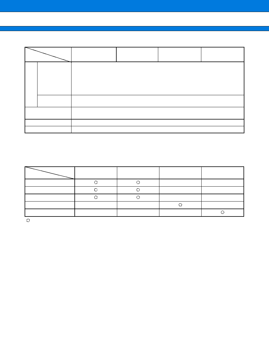
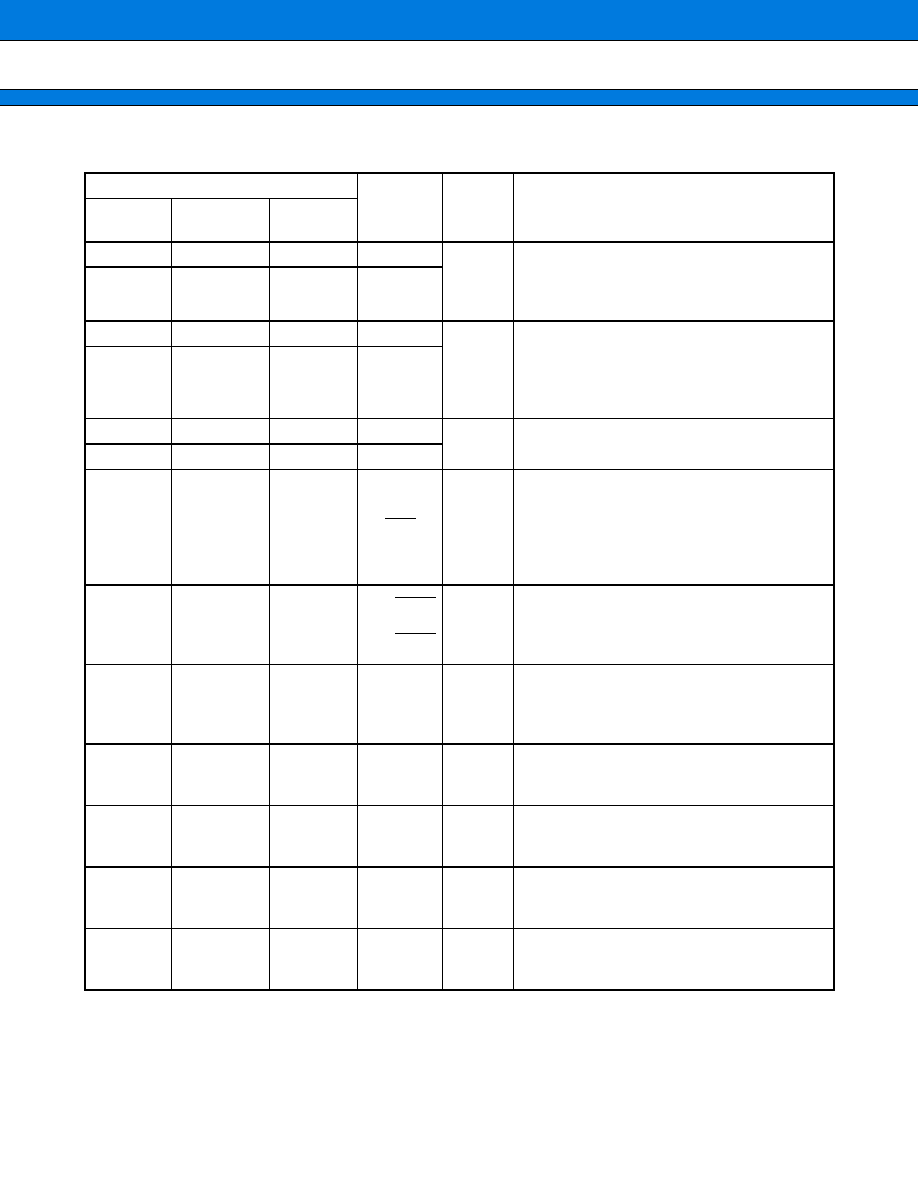
PRODUCT LINEUP
(Continued)
Part No.
Prameter
MB89965
MB89P965A
MB89F969A
MB89PV960
Classification
Mass-produced
products
(mask ROM products)
One-time product
Flash product
Piggyback/
evaluation product
for testing and
development
ROM size
16 K
◊
8-bit (Internal mask ROM)
60 K
◊
8-bit
32 K
◊
8-bit
(External ROM) *
RAM size
512
◊
8-bit
1024
◊
8-bit
CPU functions
Number of instructions
Instruction bit length
Instruction length
Data bit length
Minimum execution time
Interrupt processing time
: 136
: 8-bit
: 1 to 3 bytes
: 1-, 8-, 16bits
: 0.4
µ
s (at 10 MHz)
: 3.6
µ
s (at 10 MHz)
Pe-
riph-
eral
func-
tions
Ports
Output-only ports (N-ch open drain)
Output-only ports (CMOS)
General-purpose I/O ports (CMOS)
Total
: 6 (4 pins are shared with analog inputs)
(2 pins are shared with resource I/O)
: 8
: 21 (shared with resource I/O)
35 (max.)
Timebase timer
21-bit
Four interrupt intervals selectable 0.82 ms, 3.3 ms, 26.2 ms, or 419.4 ms (approx.) (for
main clock)
Watchdog timer
Reset trigger period : 419.4 ms (10 MHz main clock)
500 ms (32.768 MHz sub-clock)
I
2
C interface
One channel. Supports Intel SM bus (version 1.0) and Philips I
2
C bus standards.
Uses a 2-wire protocol for communications with other devices.
Included/Not included
(Specified when order-
ing. See "Ordering In-
formation" for details.)
Included
8/16-bit timer/
counter Timer
2 channel 8-bit timer/counter operation (independent operation clocks for timer 1 and
timer 2) or 16-bit timer/counter operation (operation clock period : 0.8
µ
s to 204.8
µ
s)
can execute an event counter operation and output a square wave using an external
Clock.
1 or 16-bit timer/counter operation mode
Serial I/O
8 bits
LSB-first or MSB-first selectable
Transfer clocks : External or three internal clocks (0.8
µ
s, 3.2
µ
s, 12.8
µ
s)
External
interrupt 1
(edge)
Selectable edge detection (rising, falling, or either edge)
3 independent channels
These can also be used to recover from standby modes (edge detection is still available
in stop mode) .
External
interrupt 2
(level)
1 channel with 8 inputs ("L" level interrupts, independent input enable)
This can also be used to recover from standby modes (level detection is still available in
stop mode) .
MB89960 Series
4
(Continued)
* : Use the MBM27C256A-20TVM as the external ROM (Operating voltage : 4.5 V to 5.5 V)
Note : Unless otherwise stated, clock periods and conversion times are for 10 MHz operation with the main clock
operating at maximum speed.
s
s
s
s
PACKAGES AND CORRESPONDING PRODUCTS
: Available
: Not available
Part No.
Prameter
MB89965
MB89P965A
MB89F969A
MB89PV960
Pe-
riph-
eral
func-
tions
A/D converter
4 channel
◊
10-bit resolution
A/D conversion time : 15.2
µ
s (MB89965, MB89P965A, MB89F969A)
13.2
µ
s (MB89PV960)
Continuous activation is available using the output from the 8/16-bit timer/counter or
timebase timer.
Reference voltage input (AVR)
Clock prescaler
15-bit
Interrupt interval : 31.25 ms, 0.25 s, 0.50 s, 1.00 s (for a 32.768 kHz sub-clock)
Low power consump-
tion (standby modes)
Sleep mode, stop mode, and clock mode
Process
CMOS
Operating voltage
3.5 V to 5.5 V
Package
Part No.
MB89965
MB89P965A
MB89F969A
MB89PV960
FPT-48P-M05
FPT-48P-M13
FPT-48P-M16
FPT-64P-M09
MQP-48C-P01
◊
◊
◊
◊
◊
◊
◊
◊
◊
◊
◊
◊
◊
MB89960 Series
5
s
s
s
s
DIFFERENCES AMONG PRODUCTS
1.
Memory Space
Please take note of the differences among products before testing and developing software for the MB89960
series.
∑ The RAM and ROM configurations differ among products.
∑ If the bottom stack address is set at the top RAM address, this will need to be relocated if changing to a different
product.
2.
Current Consumption
∑ In the case of the MB89PV960, add the current consumed by the EPROM which is connected to the top socket.
∑ When operated at low speed, one-time PROM and EPROM products will consume more current than mask
ROM products. However, the current consumption in sleep/stop modes is the same.
3.
Functional Differences Between MB89960 Series
4.
Mask Options
Functions that can be selected as options and the methods used to specify these options vary by the product.
Before using mask options, check section "
Mask Options".
MB89965/P965A/F969A
MB89PV960
Power-on reset delay time
Regulator stabilization delay time,
regulator recovery time,
oscillation stabilization delay time
Oscillation stabilization delay time
External reset delay time in stop/
sub-clock mode or external
interrupt delay time in main stop
mode
Regulator recovery time,
oscillation stabilization delay time
Oscillation stabilization delay time
Port pin pull-up resistors
Software-selectable
Not available
A/D conversion time
38 instruction cycles
33 instruction cycles
I
2
C noise elimination circuit
Always present regardless of ICCR :
DMPB bit setting
Disabled if ICCR : DMPB bit
=
"1"
MB89960 Series
6
s
s
s
s
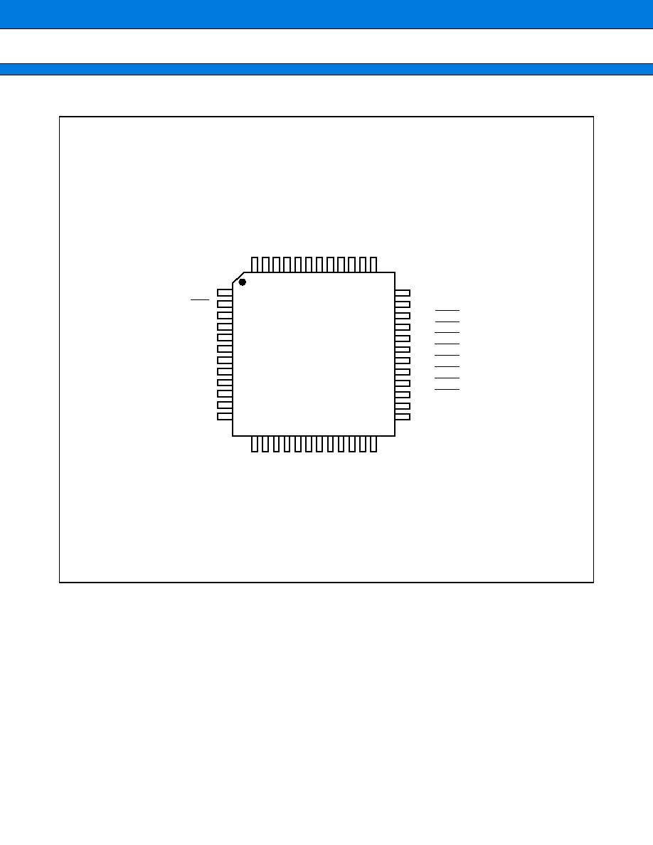
PIN ASSIGNMENT
(Continued)
(TOP VIEW)
(FPT-48P-M05)
(FPT-48P-M13)
(FPT-48P-M16)
1
2
3
4
5
6
7
8
9
10
11
12
AV
CC
RST
MOD0
MOD1
X0
X1
V
CC
X0A
X1A
P27
P26
P25
36
35
34
33
32
31
30
29
28
27
26
25
P34/TO/CLK
C
P00/INT20
P01/INT21
P02/INT22
P03/INT23
P04/INT24
P05/INT25
P06/INT26
P07/INT27
P10/INT10
P11/INT11
48
47
46
45
44
43
42
41
40
39
38
37
P40/AN0
P41/AN1
P42/AN2
P43/AN3
AVR
AV
SS
P44/SDA
P45/SCL
P30/SCK
P31/SO
P32/SI
P33/EC
13
14
15
16
17
18
19
20
21
22
23
24
P24
P23
P22
P21
P20
P17
V
SS
P16
P15
P14
P13
P12/INT12

MB89960 Series
7
(Continued)
(Continued)
(TOP VIEW)
(MQP-48C-P01)
1
2
3
4
5
6
7
8
9
10
11
12
AV
CC
RST
MOD0
MOD1
X0
X1
V
CC
X0A
X1A
P27
P26
P25
36
35
34
33
32
31
30
29
28
27
26
25
P34/TO/CLK
N.C.
P00/INT20
P01/INT21
P02/INT22
P03/INT23
P04/INT24
P05/INT25
P06/INT26
P07/INT27
P10/INT10
P11/INT11
48
47
46
45
44
43
42
41
40
39
38
37
P40/AN0
P41/AN1
P42/AN2
P43/AN3
AVR
AV
SS
P44/SDA
P45/SCL
P30/SCK
P31/SO
P32/SI
P33/EC
13
14
15
16
17
18
19
20
21
22
23
24
P24
P23
P22
P21
P20
P17
V
SS
P16
P15
P14
P13
P12/INT12
69
70
71
72
73
74
75
76
60
59
58
57
56
55
54
53
68
67
66
65
64
63
62
61
77
78
79
80
49
50
51
52
* : Pin assignment on package top (MB89PV960)
N.C. : Internally connected. Do not use.
Pin No.
Pin
Name
Pin No.
Pin
Name
Pin No.
Pin
Name
Pin No.
Pin
Name
49
V
PP
57
N.C.
65
O4
73
OE
50
A12
58
A2
66
O5
74
N.C.
51
A7
59
A1
67
O6
75
A11
52
A6
60
A0
68
O7
76
A9
53
A5
61
O1
69
O8
77
A8
54
A4
62
O2
70
CE
78
A13
55
A3
63
O3
71
A10
79
A14
56
N.C.
64
V
SS
72
N.C. 80
V
CC

MB89960 Series
8
(Continued)
(TOP VIEW)
(FPT-64P-M09)
N.C.
N.C.
P40/AN0
P41/AN1
P42/AN2
P43/AN3
AVR
AV
SS
P44/SDA
P45/SCL
P30/SCK
P31/SO
P32/SI
P33/EC
N.C.
N.C.
17
18
19
20
21
22
23
24
25
26
27
28
29
30
31
32
1
48
N.C.
2
47
N.C.
3
46
P34/TO/CLK
4
45
C
5
44
P00/INT20
6
43
P01/INT21
7
42
P02/INT22
8
41
P03/INT23
9
40
P04/INT24
10
39
P05/INT25
11
38
P06/INT26
12
37
P07/INT27
13
36
P10/INT10
14
35
P11/INT11
15
34
N.C.
16
33
N.C.
N.C.
N.C.
P24
P23
P22
P21
P20
P17
V
SS
P16
P15
P14
P13
P12/INT12
N.C.
N.C.
64
63
62
61
60
59
58
57
56
55
54
53
52
51
50
49
TEST
MOD2
AV
CC
RST
MOD0
MOD1
X0
X1
V
CC
X0A
X1A
P27
P26
P25
N.C.
N.C.
MB89960 Series
9
s
s
s
s
PIN DESCRIPTIONS
*1 : FPT-48P-M05
*2 : FPT-48P-M16, FPT-48P-M13
*3 : MQP-48C-P01
*4 : FPT-64P-M09
Pin No.
Pin Name
Circuit
Type
Function
MQFP-48*
3
LQFP-48*
1
QFP-48*
2
LQFP-64*
4
5
5
7
X0
A
Oscillator connection pins for the main clock os-
cillator (crystal oscillator or similar) .
When using an external clock, input the clock
signal to X0 and leave X1 open.
6
6
8
X1
8
8
10
X0A
B
Oscillator connection pins for the sub-clock os-
cillator (crystal oscillator or similar) .
When using an external clock (low speed :
32.768 kHz) , input the clock signal to X0A and
leave X1A open.
9
9
11
X1A
3
3
5
MOD0
C
Input pins for setting the memory access mode.
Connect directly to V
SS
.
4
4
6
MOD1
2
2
4
RST
D
Reset I/O pin
This is an N-ch open-drain output type with pull-
up resistor and a hysteresis input type. The pin
outputs "L" when an internal reset is present.
Similarly, inputting "L" initializes the internal cir-
cuits.
27 to 34
27 to 34
37 to 44
P00/INT20
to
P07/INT27
E
General-purpose I/O ports
Also serves as the external interrupt 2 inputs
(wakeup inputs) . The external interrupt 2 inputs
are hysteresis inputs.
24 to 26
24 to 26
30,
35,
36
P10/INT10
to
P12/INT12
E
General-purpose I/O ports
Also serves as the external interrupt 1 inputs
(wakeup inputs) . The external interrupt 1 inputs
are hysteresis inputs.
18,
20 to 23
18,
20 to 23
24,
26 to 29
P13
to
P17
E
General-purpose I/O ports
10 to 17
10 to 17
12 to 14
19 to 23
P20
to
P27
G
General-purpose outoput-only ports
40
40
54
P30/SCK
F
General-purpose I/O port
Also serves as the serial clock I/O.
A hysteresis input.
39
39
53
P31/SO
F
General-purpose I/O port
Also serves as the serial I/O data output.
A hysteresis input.
(Continued)

MB89960 Series
10
(Continued)
*1 : FPT-48P-M05
*2 : FPT-48P-M16, FPT-48P-M13
*3 : MQP-48C-P01
*4 : FPT-64P-M09
Pin No.
Pin Name
Circuit
Type
Function
MQFP-48*
3
LQFP-48*
1
QFP-48*
2
LQFP-64*
4
38
38
52
P32/SI
F
General-purpose I/O port
Also serves as the serial I/O data input.
A hysteresis input.
37
37
51
P33/EC
F
General-purpose I/O port
Also serves as the external clock input for the 8/
16-bit timer/counter. A hysteresis input.
36
36
46
P34/TO/
CLK
F
General-purpose I/O port
Also serves as the overflow output for the 8/16-
bit timer/counter and the CLK clock
output. A hysteresis input.
35
45
C
Connect a 0.1
µ
F capacitor on the MB89965,
MB89P965A, and MB89F969A.
45 to 48
45 to 48
59 to 62
P40/AN0
to
P43/AN3
H
General-purpose Nch open-drain outputs.
Also serves as the A/D converter analog inputs.
42
42
56
P44/SDA
I
General-purpose Nch open-drain output.
Also serves as the I
2
C interface data output.
41
41
55
P45/SCL
I
General-purpose Nch open-drain output.
Also serves as the I
2
C interface clock I/O.
7
7
9
V
CC
Power supply pin
19
19
25
V
SS
Power supply (GND) pin
1
1
3
AV
CC
A/D converter power supply pin
Use this pin at the same voltage as V
CC
.
44
44
58
AVR
A/D converter reference voltage input pin
43
43
57
AV
SS
A/D converter power supply pin
Use this pin at the same voltage as V
SS
.
35
15 to 18
31 to 34
47 to 50
63, 64
N.C.
These pins are not connected.
Do not connect these on the MB89PV960.
1
TEST
C
TEST pin. Connect directly to V
SS
.
Only used on the MB89F969A.
Treat as an N.C. pin on the MB89965.
2
MOD2
C
Memory access mode setting pin. Connect di-
rectly to V
SS
.
Only used on the MB89F969A.
Treat as an N.C. pin on the MB89965.

MB89960 Series
11
∑ Pin Descriptions for External EPROM (MB89PV960 only)
Pin No.
Pin Name
I/O
Function
49
Vpp
O
"H" level output pin
50
51
52
53
54
55
A12
A7
A6
A5
A4
A3
O
Address output pins
58
59
60
A2
A1
A0
O
Address output pins
61
62
63
O1
O2
O3
I
Data input pins
64
V
SS
Power supply (GND) pin
65
66
67
68
69
O4
O5
O6
O7
O8
I
Data input pins
70
CE
O
ROM chip enable pin
Outputs "H" during standby mode.
71
A10
O
Address output pin
73
OE
O
ROM output enable pin
Always outputs "L".
75
76
77
78
79
A11
A9
A8
A13
A14
O
Address output pins
80
V
CC
EPROM power supply pin
56
57
72
74
N.C.
Internally connected pins
Always leave open circuit.
MB89960 Series
12
s
s
s
s
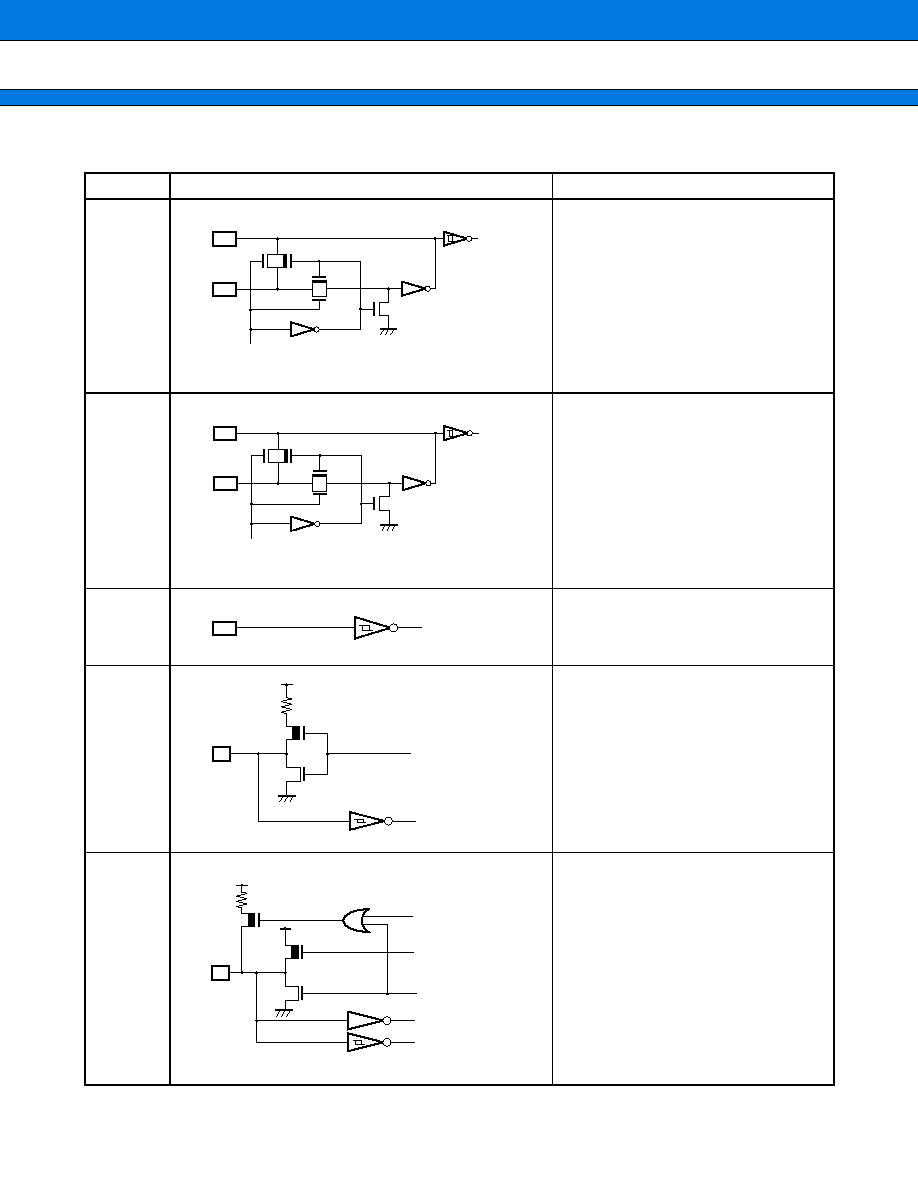
I/O CIRCUIT TYPE
(Continued)
Type
Circuit
Remarks
A
High speed clock (main clock oscillation)
∑ Oscillation feedback resistor
B
Low speed clock (sub-clock oscillation)
∑ Oscillation feedback resistor
C
∑ CMOS input
D
∑ Output pull-up resistor (Pch)
approx. 50 k
(at 5 V)
∑ Hysteresis input
E
∑ CMOS output
∑ CMOS input
∑ Selectable pull-up resistor
approx. 50 k
(at 5 V)
Nch
Nch
X1
X0
Pch
Pch
Main clock control signal
Nch
Nch
Nch
X1A
X0A
Pch
Pch
Sub-clock control signal
R
Pch
Nch
Pch
Pch
Pull-up
Port
Resource
Nch
R

MB89960 Series
13
(Continued)
Type
Circuit
Remarks
F
∑ CMOS output
∑ Hysteresis input
∑ Selectable pull-up resistor
approx. 50 k
(at 5 V)
G
∑ CMOS output
H
∑ Nch-open drain output
∑ Analog input (A/D converter)
∑ Selectable pull-up resistor
∑ (The pull-up resistor cannot be used
when used as an analog input.)
approx. 50 k
(at 5 V)
I
∑ Nch open drain output
∑ Selectable SMB or I
2
C
input buffer
Pch
Pull-up
Resource
Pch
Nch
R
Pch
Nch
Pch
Pull-up
Analog input
Nch
R
Nch
SMB buffer
I
2
C buffer
SMB input
I
2
C input

MB89960 Series
14
s
s
s
s
HANDLING DEVICES
1.
Do not exceed maximum rated voltage (to prevent latch-up)
Latch-up may occur on CMOS ICs if voltage higher than V
CC
or lower than V
SS
is applied to input or output pins
other than medium- and high voltage pins or if the voltage applied between V
CC
and V
SS
higher the rating.
If latch-up occurs, the power supply current increases rapidly resulting in thermal damage to circuit elements.
Therefore, ensure that maximum ratings are not exceeded in circuit operation.
Similarly, when turning the analog power supply on or off, ensure the analog power supply voltages (AV
CC
and
AVR) and analog input voltages do not exceed the digital power supply (V
CC
) .
2.
Power supply voltage fluctuations
Rapid fluctuation of the voltage may cause the device to misoperate, even if the voltage remains within the
allowed operating range.
The standard for power supply voltage stability is a peak-to-peak V
CC
ripple voltage at the mains supply frequency
(50 to 60 Hz) of 10
%
or less of V
CC
and a transient voltage change rate of 0.1 V/ms or less such as when turning
the power supply on or off.
3.
Treatment of unused input pins
Leaving unused input pins unconnected can cause misoperation or permanent damage to the device due to
latchup. Always pull-up or pull-down unused input pins using a 2 k
or larger resistor.
If some I/O pins are unused, either set as outputs and leave open circuit or set as inputs and treat in the same
way as input pins.
4.
Treatment of N.C. pins
Always leave N.C. (internally connected) pins open.
5.
Treatment of power supply pins on microcontrollers with an A/D converter
Even if not using the A/D converter, connect to be AV
CC
=
V
CC
and AV
SS
=
AVR
=
V
SS
.
6.
Precautions on using an external clock
An oscillation stabilization delay occurs after a power-on reset or when recovering from sub-clock or stop mode,
even if an external clock is used.
MB89960 Series
15
s
s
s
s
PROGRAMMING SPECIFICATIONS FOR ONE-TIME PROM PRODUCTS
The MB89P965A has a "PROM mode" that enables the microcontroller to be programmed using a general-
purpose ROM programmer via a special adaptor. Note, however, that electronic signature mode is not available.
1.
ROM Programmer Adaptor and Recommended ROM Writers
∑ Enquiries
Sun Hayato Co. Ltd. : TEL
03-3986-0403
Ando Denki Co. Ltd. : TEL
044-549-7300
2.
PROM Mode Memory Map
3.
PROM Programming Procedure (When using an Ando EPROM programmer)
1) Set the EPROM programmer type code to 17209.
2) Load the program data into addresses 0000
H
to 3FFF
H
in the EPROM programmer.
3) Use the EPROM programmer to program to addresses C000
H
to FFFF
H
.
4.
Programming Yield
Due to the nature of OTPROM memory, a program test to all bits on a blank OTPROM microcontroller cannot
be performed at Fujitsu. For this reason, a programming yield of 100
%
cannot be assured at all times.
Package Name
Adaptor Part No.
Recommended Programmer Manufacturer and Model
Sun Hayato Co. Ltd.
Ando Denki Co. Ltd.
FPT-48P-M05
ROM2-48LQF-32DP-8LA
AF9708 (ver 1.44 or later)
AF9709 (ver 1.44 or later)
FPT-48P-M13
ROM2-48QF2-32DP-8LA
FPT-48P-M16
ROM2-48QF-32DP-8LA
0000
H
3FFF
H
0000
H
FFFF
H
RAM
PROM mode
(addresses on ROM programmer)
Not available
Program
area
(PROM)
Program
area
(PROM)
General-
purpose
registers
I/O
Normal operating mode
0080
H
0280
H
C000
H
0200
H
0100
H

MB89960 Series
16
s
s
s
s
PROGRAMMING AND ERASING FLASH MEMORY ON THE MB89F969A
1.
Flash Memory
The flash memory is located between 1000
H
and FFFF
H
in the CPU memory map and incorporates a flash
memory interface circuit that allows read access and program access from the CPU to be performed in the same
way as mask ROM. Programming and erasing flash memory is also performed via the flash memory interface
circuit by executing instructions in the CPU. This enables the flash memory to be updated in place under the
control of the CPU, providing an efficient method of updating program and data.
2.
Flash Memory Features
∑ 60 K byte
◊
8-bit configuration (16 K
+
8 K
+
8 K
+
28 K sectors)
∑ Automatic programming algorithm (Embedded algorithm* : Equivalent to MBM29LV200)
∑ Includes an erase pause and restart function
∑ Data polling and toggle bit for detection of program/erase completion
∑ Detection of program/erase completion via CPU interrupt
∑ Compatible with JEDEC-standard commands
∑ Sector Protection (sectors can be combined in any combination)
∑ No. of program/erase cycles : 10,000 (min.)
Embedded Algorithm is a trademark of Advanced Micro Devices.
3.
Procedure for Programming and Erasing Flash Memory
Programming and reading flash memory cannot be performed at the same time. Accordingly, to program or
erase flash memory, the program must first be copied from flash memory to RAM so that programming can be
performed without program access from flash memory.
4.
Flash Memory Register
∑ Control status register (FMCS)
5.
Sector Configuration
The table below shows the sector configuration of flash memory and lists the addresses of each sector for both
during CPU access a flash memory programming.
∑ Sector configuration of flash memory
* : Programmer address
The programmer address is the address to be used instead of the CPU address when programming data from
a parallel flash memory programmer. Use the programmer address on programming or erasing using a general-
purpose parallel programmer.
Flash Memory
CPU Address
Programmer Address
16 K bytes
FFFF
H
to C000
H
1FFFF
H
to 1C000
H
8 K bytes
BFFF
H
to A000
H
1BFFF
H
to 1A000
H
8 K bytes
9FFF
H
to 8000
H
19FFF
H
to 18000
H
28 K bytes
7FFF
H
to 1000
H
17FFF
H
to 11000
H
R
R/W
R/W
RDY
bit7
bit6
bit5
bit4
bit3
bit2
bit1
bit0
002E
H
Address
000X00-0
B
Initial value
Reserved Reserved
Reserved
R/W
R/W
R/W
R/W
INTE
RDYINT
WE

MB89960 Series
17
6.
ROM Programmer Adaptor and Recommended ROM Programmers
∑ Enquiries
Sun Hayato Co. Ltd. : TEL
03-3986-0403
Ando Denki Co. Ltd. : TEL
044-549-7300
Package Name
Adaptor Part No.
Recommended Programmer Manufacturer and Model
Sun Hayato Co. Ltd.
Ando Denki Co. Ltd.
FPT-64P-M09
FLASH-64QF2-32DP-8LF
AF9708 (ver 1.60 or later)
AF9709 (ver 1.60 or later)

MB89960 Series
18
s
s
s
s
PROGRAMMING A PIGGYBACK/EVALUATION EPROM
1.
EPROM Type
MBM27C256A-20TVM
2.
Programming Adaptor
Use the following programming adaptor (made by Sun Hayato Co. Ltd.) to program the EPROM using a ROM
programmer.
∑ Programming adaptor
Enquiries
Sun Hayato Co. Ltd. : TEL03-3986-0403
3.
Memory Space
4.
EPROM Programming Procedure
(1) Setup the EPROM programmer to the MBM27C256A.
(2) Load the program data into addresses 0000
H
to 7FFF
H
in the EPROM programmer.
(3) Use the ROM programmer to program to addresses 0000
H
to 7FFF
H
.
Package
Adaptor Socket Part No.
LCC-32 (Square)
ROM-32LC-28DP-S
0000
H
7FFF
H
0000
H
FFFF
H
RAM
I/O
Not available
Program
area
(PROM)
EPROM mode
(addresses on ROM programmer)
Program
area
(PROM)
Normal operating mode
0080
H
8000
H
0280
H
MB89960 Series
19
s
s
s
s
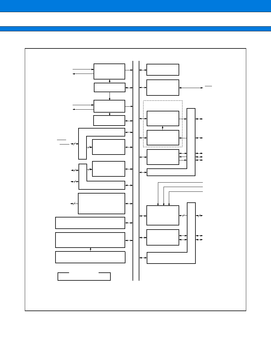
BLOCK DIAGRAM
F
2
MC-8L
R A M
MOD0, MOD1, Vcc, Vss, C
Other pins
RST
P00/INT20
to P07/INT27
R O M
P32/SI
P34/TO/CLK
C P U
P33/EC
P31/SO
P30/SCK
P44/SDA
P45/SCL
X0
Main clock
Sub-clock
Clock control
Timebase timer
Reset circuit
(watchdog timer)
16-bit
timer/counter
8-bit
timer/counter 2
8-bit
timer/counter 1
8-bit
serial I/O
10-bit
A/D converter
I
2
C interface
Nch open drain
output port
CMOS I/O port
Clock prescaler
External interrupt 2
(Level)
External interrupt 1
(edge)
CMOS I/O port
CMOS I/O port
CMOS output port
Port 0
Port 3
Port 4
Internal data bus
Port 1
Port 2
Low speed
oscillator circuit
(32.768 kHz)
High speed
oscillator circuit
(Max. 10 MHz)
X1
8
P13 to P17
3
X0A
X1A
P20 to P27
8
3
8
4
4
AVR
AV
CC
AV
SS
5
P10/INT10
to P12/INT12
P40/AN0
P43/AN3
MB89960 Series
20
s
s
s
s
CPU CORE
1.
Memory Space
(1) Structure of memory space
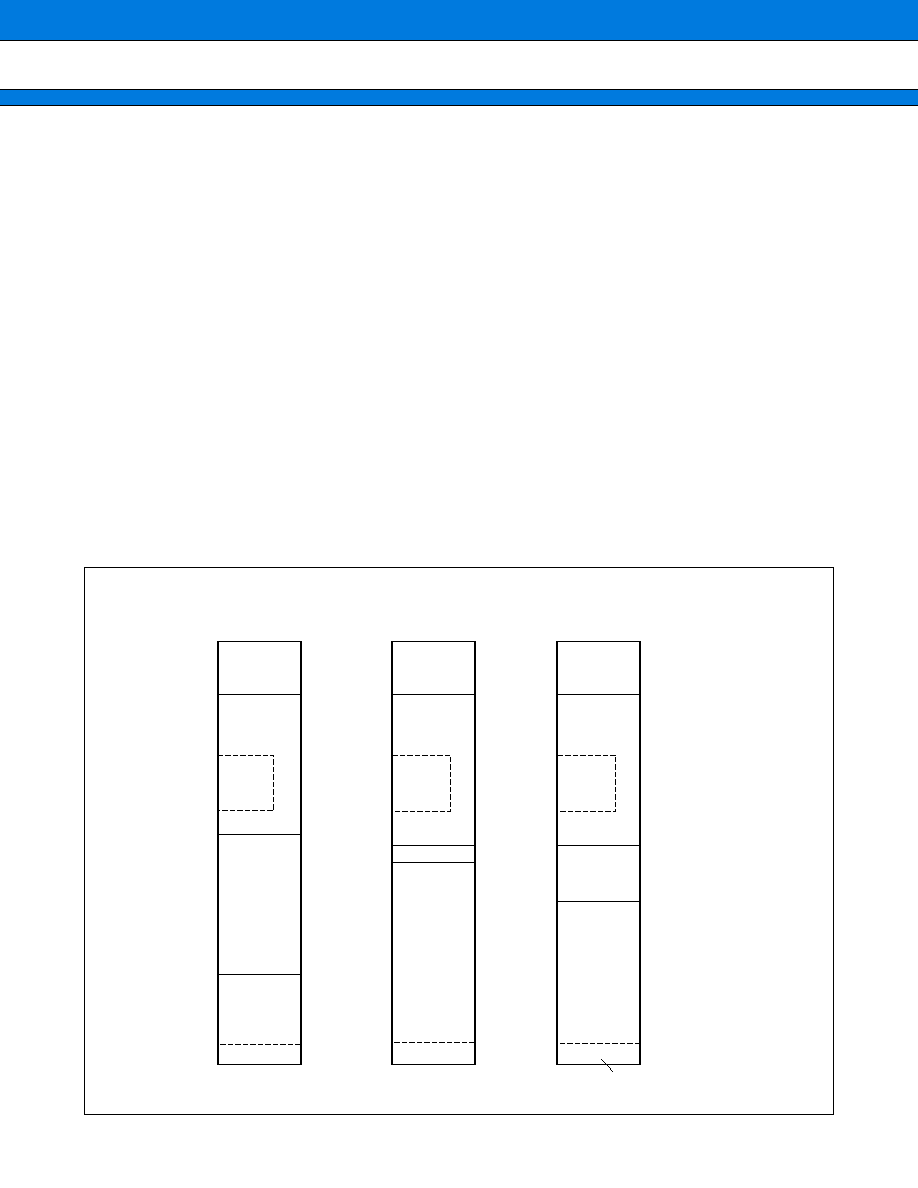
∑ I/O area (address : 0000
H
to 007F
H
)
∑ Assign the control registers, data registers, and similar of the internal peripheral functions.
∑ As the I/O area is allocated as part of the memory space, it can be accessed in the same way as memory.
Direct addressing also provides high speed access.
∑ RAM area
∑ Static RAM is provided as an internal data area.
∑ The size of internal RAM differs between products.
∑ Addresses 80
H
to FF
H
provide high speed access using direct addressing.
∑ Addresses 100
H
to 1FF
H
are used as the general-purpose register area.
∑ The initial value of RAM after a reset is undefined.
∑ ROM area
∑ ROM memory is provided as the internal program area.
∑ The size of internal ROM differs between products.
∑ Addresses FFC0
H
to FFFF
H
are used for the vector table and similar.
(2) Memory map
0000
H
0080
H
0100
H
8000
H
MB89PV960
I/O
RAM
ROM
Vector table
(Reset, interrupt, vector call instruction)
0000
H
0080
H
0100
H
0200
H
C000
H
FFFF
H
MB89965
MB89P965A
I/O
RAM
ROM
FFFF
H
0280
H
0200
H
0480
H
FFC0
H
FFC0
H
0000
H
0080
H
0100
H
1000
H
MB89F969A
I/O
RAM
Not available
Not available
Not available
Registers
Registers
Registers
ROM
FFFF
H
0200
H
0480
H
FFC0
H
MB89960 Series
21
2.
Registers
The MB89960 series provides two types of registers: dedicated registers in the CPU and general-purpose
registers. The dedicated registers are as follows.
The upper 8 bits of the PS contain the register bank pointer (RP) and the lower 8 bits contain the condition code
register (CCR) . (See the diagram below.)
Program counter (PC)
: A 16-bit register for indicating the instruction storage positions.
Accumulator (A)
: A 16-bit register that provides temporary storage for arithmetic operations and
similar. Instructions that operate on 8-bit data use the lower byte.
Temporary accumulator (T) : A 16-bit register used for arithmetic operations with the accumulator. Instructions
that operate on 8-bit data use the lower byte.
Index register (IX)
: A 16-bit register used for index modification.
Extra pointer (EP)
: A 16-bit pointer used for indicating a memory address .
Stack pointer (SP)
: A 16-bit register used for indicating a stack area.
Program status (PS)
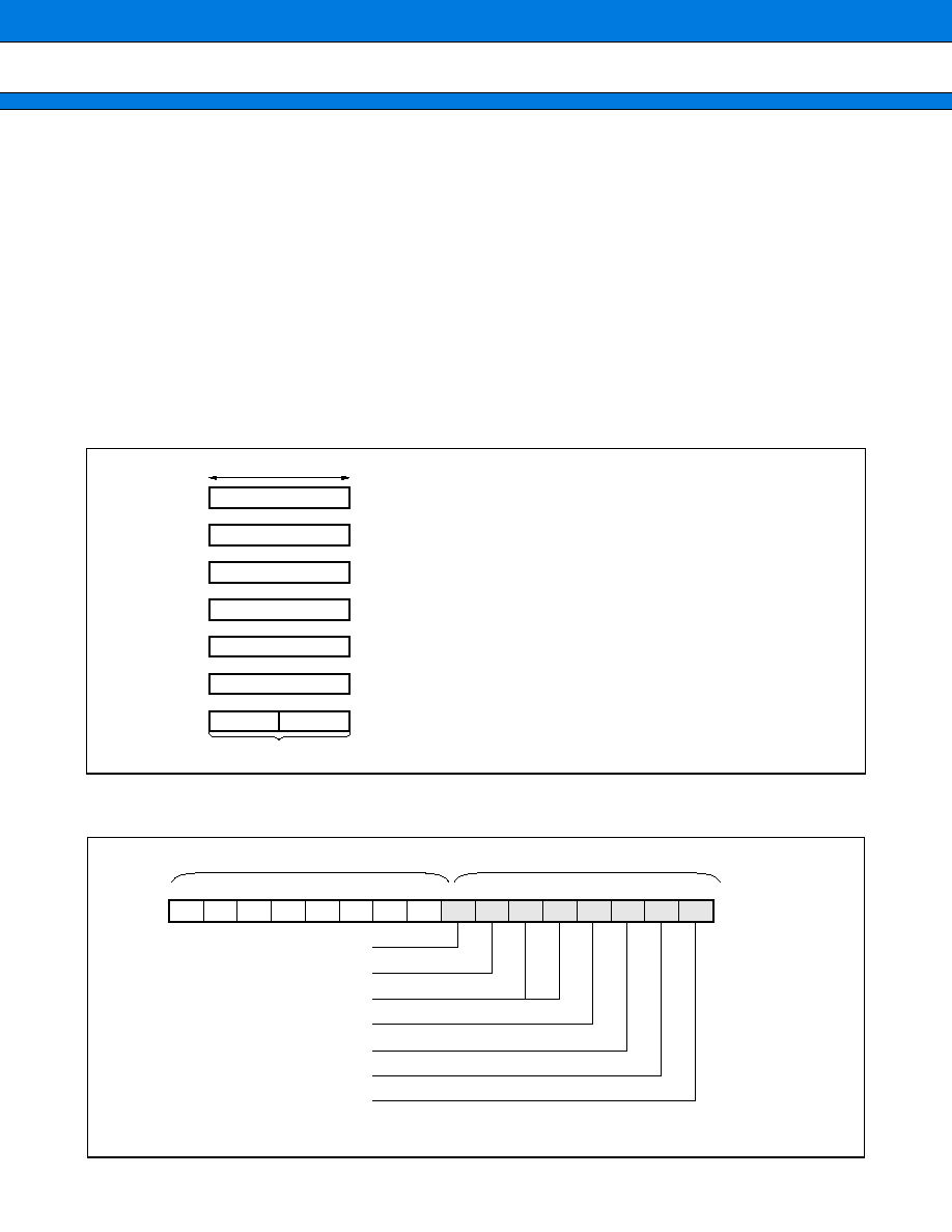
: A 16-bit register used to store a register pointer and condition code.
PS
16 bits
Initial value
PC
A
T
IX
EP
SP
: Program counter
: Accumulator
: Temporary accumulator
: Index register
: Extra pointer
: Stack pointer
RP
CCR
: Program status
FFFD
H
Undefined
Undefined
Undefined
Undefined
Undefined
I flag = 0, IL1, IL0 = 11
Other bits are undefined
PS
X : Undefined
Half carry flag
Interrupt enable flag
Interrupt level bits
Negative flag
Zero flag
Overflow flag
Carry flag
RP
CCR
X011XXXX
B
CCR Initial value
bit15 bit14 bit13 bit12 bit11 bit10
bit9
bit8
bit7
bit6
bit5
bit4
bit3
bit2
bit1
bit0
R4
R3
R2
R1
R0
-
-
-
H
I
IL1
IL0
N
Z
V
C

MB89960 Series
22
The RP contains the address of the currently used register bank. The conversion diagram below shows the
relationship between the RP value and actual address.
CCR contains bits that indicate the result of an arithmetic operation or information about transfer data and bits
used to control CPU operation when an interrupt occurs.
H-flag
: Set to "1" when a carry from bit 3 to bit 4 or a borrow from bit 4 to bit 3 occurs as a result of an
arithmetic operation. Cleared to "0" otherwise. This flag is for decimal adjustment instructions and
should be ignored for operations other than addition and subtraction.
I-flag
: Interrupts are enabled when this flag is set to "1" and disabled when the flag is set to "0". Cleared
to "0" by a reset.
IL1, 0
: Indicates the level of interrupts currently allowed. The CPU only processes interrupts with a re-
quest level higher than the value indicated by these bits.
IL1
IL0
Interrupt Level
Priority
0
0
1
High
Low
=
No interrupt
0
1
1
0
2
1
1
3
N-flag
: Set to "1" when the MSB of the result of an arithmetic operation is "1" and cleared to "0" when the
MSB is "0".
Z-flag
: Set to "1" when the result of an arithmetic operation is zero. Cleared to "0" otherwise
V-flag
: Set to "1" when a 2's complement overflow occurs as the result of an arithmetic operation. Cleared
to "0" if no 2's complement overflow occurs.
C-flag
: Set to "1" when a carry from bit 7 or a borrow to bit 7 occurs as the result of an arithmetic opera-
tion. Cleared to "0" otherwise. Set to the shift-out value in the case of a shift instruction.
"0"
"0"
"0"
"0"
"0"
"0"
"0"
"1"
R4
R3
R2
R1
R0
b2
b1
b0
A7
A6
A5
A4
A3
A2
A1
Upper (RP)
Lower (op code)
A0
A15
Actual address
A14 A13 A12 A11 A10
A9
A8
Rules for converting of actual addresses of the general-purpose register area

MB89960 Series
23
The following general-purpose registers are provided :
General-purpose registers : 8-bit resisters for storing data
The general-purpose registers are 8-bit registers and are allocated in the register banks of the memory. Each
bank contains 8 registers and all 32 banks can be used on MB89960 series microcontrollers.
The register bank pointer (RP) specifies the bank that is currently in use.
R0
Address
=
0100
H
+
8
◊
(RP)
R1
R2
R3
R4
R5
R6
R7
Memory area
32 banks
Register bank structure

MB89960 Series
24
s
s
s
s
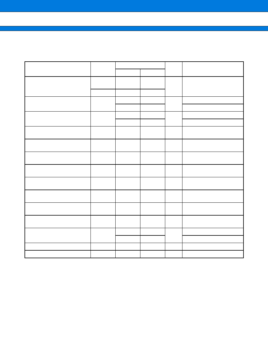
I/O MAP
(Continued)
Address
Abbreviation
Register Name
Read/Write
Initial Value
00
H
PDR0
Port 0 data register
R/W
XXXXXXXX
B
01
H
DDR0
Port 0 direction register
W
0
0
0
0
0
0
0
0
B
02
H
PDR1
Port 1 data register
R/W
XXXXXXXX
B
03
H
DDR1
Port 1 direction register
W
0
0
0
0
0
0
0
0
B
04
H
PDR2
Port 2 data register
R/W
0
0
0
0
0
0
0
0
B
05
H
(Unused area)
06
H
07
H
SYCC
System clock control register
R/W
X
-
-
MM1
0
0
B
08
H
STBC
Standby control register
R/W
0
0
0
1
0
-
-
-
B
09
H
WDTC
Watchdog control register
R/W
0
-
-
-
XXXX
B
0A
H
TBTC
Timebase timer control register
R/W
0
0
-
-
-
0
0
0
B
0B
H
WPCR
Clock prescaler control register
R/W
0
0
-
-
-
0
0
0
B
0C
H
PDR3
Port 3 data register
R/W
-
-
-XXXXX
B
0D
H
DDR3
Port 3 direction register
R/W
-
-
0
0
0
0
0
0
B
0E
H
PDR4
Port 4 data register
R/W
-
-
1
1
1
1
1
1
B
0F
H
(Unused area)
10
H
IBSR
I
2
C bus status register
R
0
0
0
0
0
0
0
0
B
11
H
IBCR
I
2
C bus control register
R/W
0
0
0
1
1
0
0
0
B
12
H
ICCR
I
2
C clock control register
R/W
0
0
0XXXXX
B
13
H
IADR
I
2
C address register
R/W
-
XXXXXXX
B
14
H
IDAR
I
2
C data register
R/W
XXXXXXXX
B
15
H
(Unused area)
16
H
17
H
18
H
T2CR
Timer 2 control register
R/W
X0
-
-
XXX0
B
19
H
T1CR
Timer 1 control register
R/W
X0
0
0XXX0
B
1A
H
T2DR
Timer 2 data register
R/W
XXXXXXXX
B
1B
H
T1DR
Timer 1 data register
R/W
XXXXXXXX
B
1C
H
SMR
Serial mode register
R/W
0
0
0
0
0
0
0
0
B
1D
H
SDR
Serial data register
R/W
XXXXXXXX
B
1E
H
(Unused area)
1F
H
20
H
ADC1
A/D control register 1
R/W
0
0
0
0
0
0
-
0
B
21
H
ADC2
A/D control register 2
R/W
-
0
0
0
0
0
0
1
B
22
H
ADDH
A/D data register H
R/W
- - - - - - XX
B

MB89960 Series
25
(Continued)
∑ Read/write notation
∑ Initial value notation
Note : Do not use the "unused areas".
Address
Abbreviation
Register Name
Read/Write
Initial Value
23
H
ADDL
A/D data register L
R/W
XXXXXXXX
B
24
H
EIC1
External interrupt 1 control register 1
R/W
0
0
0
0
0
0
0
0
B
25
H
EIC2
External interrupt 1 control register 2
R/W
-
-
-
-
0
0
0
0
B
26
H
to 27
H
(Unused area)
28
H
PURR1
Pull-up resistor register 1
(MB89965, P965A, and F969A only)
R/W
1
1
1
1
1
1
1
1
B
29
H
PURR2
Pull-up resistor register 2
(MB89965, P965A, and F969A only)
R/W
1
1
1
1
1
1
1
1
B
2A
H
PURR3
Pull-up resistor register 3
(MB89965, P965A, nd F969A only)
R/W
XXX1
1
1
1
1
B
2B
H
PURR4
Pull-up resistor register 4
(MB89965, P965A, and F969A only)
R/W
XXXX1
1
1
1
B
2C
H
to 31
H
(Unused area)
32
H
EIE2
External interrupt 2 control register
R/W
0
0
0
0
0
0
0
0
B
33
H
EIF2
External interrupt 2 flag register
R/W
- - - - - - - 0
B
34
H
to 7B
H
(Unused area)
7C
H
ILR1
Interrupt level setting register 1
W
1
1
1
1
1
1
1
1
B
7D
H
ILR2
Interrupt level setting register 2
W
1
1
1
1
1
1
1
1
B
7E
H
ILR3
Interrupt level setting register 3
W
1
1
1
1
1
1
1
1
B
7F
H
ITR
Interrupt test register
Not available
XXXXXX0
0
B
R/W : Reading and writing available
R
: Read-only
W
: Write-only
0
: Initial value of bit is "0".
1
: Initial value of bit is "1".
X
: Initial value of bit is undefined.
M
: Initial value of bit is specified by mask option.
-
: Bit is not used.
MB89960 Series
26
s
s
s
s
ELECTRICAL CHARACTERISTICS
1.
Absolute Maximum Ratings
(AV
SS
=
V
SS
=
0.0 V)
* : Set AV
CC
to the same potential as V
CC
.
Also ensure that AV
CC
does not exceed V
CC
at power on.
WARNING: Semiconductor devices can be permanently damaged by application of stress (voltage, current,
temperature, etc.) in excess of absolute maximum ratings. Do not exceed these ratings.
Parameter
Symbol
Rating
Unit
Remarks
Min.
Max.
Power supply voltage
V
CC
AV
CC
V
SS
-
0.3
V
SS
+
6.0
V
*
AVR
V
SS
-
0.3
V
SS
+
6.0
Input voltage
V
I
V
SS
-
0.3
V
CC
+
0.3
V
Pins other than P44 and P55
V
SS
-
0.3
V
SS
+
6.0
Pins P44 and P45
Output voltage
V
O
V
SS
-
0.3
V
CC
+
0.3
V
Pins other than P44 and P55
V
SS
-
0.3
V
SS
+
6.0
Pins P44 and P45
"L" level maximum
output current
I
OL
15
mA
"L" level average
output current
I
OLAV
4
mA
Average value (operating cur-
rent
◊
operating ratio)
"L" level total maximum
output current
I
OL
100
mA
"L" level total average
output current
I
OLAV
40
mA
Average value (operating cur-
rent
◊
operating ratio)
"H" level maximum
output current
I
OH
-
15
mA
"H" level average
output current
I
OHAV
-
4
mA
Average value (operating cur-
rent
◊
operating ratio)
"H" level total maximum
output current
I
OH
-
50
mA
"H" level total average
output current
I
OHAV
-
20
mA
Average value (operating cur-
rent
◊
operating ratio)
Power consumption
P
D
300
mW
450
MB89F969A only
Operating temperature
T
A
-
40
+
85
∞
C
Storage temperature
Tstg
-
55
+
150
∞
C

MB89960 Series
27
2.
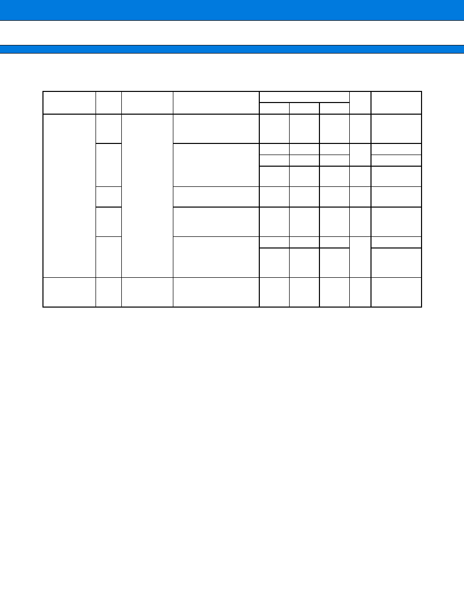
Recommended Operating Conditions
(AV
SS
=
V
SS
=
0.0 V)
* : Differs depending on the operating frequency and analog guaranteed range. See the figure below and
"5. Electrical Characteristics for the A/D Converter".
The figure above shows the frequency of the external oscillator when the instruction cycle setting is 4/F
C
. As the
operating voltage depends on the instruction cycle, change to the new instruction cycle value if using the gear
function to change the operating speed.
WARNING: The recommended operating conditions are required in order to ensure the normal operation of the
semiconductor device. All of the device's electrical characteristics are warranted when the device is
operated within these ranges.
Always use semiconductor devices within their recommended operating condition ranges. Operation
outside these ranges may adversely affect reliability and could result in device failure.
No warranty is made with respect to uses, operating conditions, or combinations not represented on
the data sheet. Users considering application outside the listed conditions are advised to contact their
FUJITSU representatives beforehand.
Parameter
Symbol
Value
Unit
Remarks
Min.
Max.
Power supply voltage
V
CC
AV
CC
3.5*
5.5*
V
Normal operation guaranteed range
(MB89965/P965A/F969A)
3.0
5.5
V
To maintain RAM state in stop mode
(MB89965/P965A/F969A)
2.7*
5.5*
V
Normal operation guaranteed range
(MB89PV960)
1.5
5.5
V
To maintain RAM state in stop mode
(MB89PV960)
AVR
3.5
AV
CC
V
Operating temperature
T
A
-
40
+
85
∞
C
6
5
4
3
2
3.5
2.7
1
2
3
4
5
Operating Frequency (MHz)
Operation guaranteed range
Analog accuracy guaranteed range : V
CC
=
AV
CC
=
3.5 V to 5.5 V
: MB89PV960
Operating Voltage (V)
6
7
8
9
10
: MB89965, MB89P965A, and MB89F969A
Operating Voltage
-
Operating frequency
MB89960 Series
28
3.
DC Characteristics
(AV
CC
=
V
CC
=
5.0 V, AV
SS
=
V
SS
=
0.0 V, T
A
=
-
40
∞
C to
+
85
∞
C)
(Continued)
Parameter
Sym-
bol
Pin Name
Condition
Value
Unit
Remarks
Min.
Typ.
Max.
"H" level input
voltage
V
IH
P00 to P07,
P10 to P17,
P30 to P34
0.7 V
CC
V
CC
+
0.3
V
V
IHS
RST, INT20 to
INT27, INT10 to
INT12, SI, SCK,
EC, TEST
0.8 V
CC
V
CC
+
0.3
V
V
IHM
MOD0/1/2
V
CC
-
0.3
V
CC
+
0.3
V
MOD pin
input
V
IHSMB
SCL, SDA
V
SS
+
1.4
V
SS
+
5.5
V
When SMB
selected
V
IHI2C
0.7 V
CC
V
SS
+
5.5
V
When I
2
C
selected
"L" level input
voltage
V
IL
P00 to P07,
P10 to P17,
P30 to P34
V
SS
-
0.3
0.3 V
CC
V
V
ILS
RST, INT20 to
INT27, INT10 to
INT12, SI, SCK,
EC, TEST
V
SS
-
0.3
0.2 V
CC
V
V
ILM
MOD0/1/2
V
SS
-
0.3
V
SS
+
0.3
V
MOD pin
input
V
ILSMB
SCL, SDA
V
SS
-
0.3
V
SS
+
0.6
V
When SMB
selected
V
ILI2C
V
SS
-
0.3
0.3 V
CC
V
When I
2
C
selected
Voltage applied to
open drain output
pins
V
D
P40 to P45
V
SS
-
0.3
V
CC
+
0.3
V
"H" level output
voltage
V
OH
P00 to P07,
P10 to P17,
P20 to P27,
P30 to P34
I
OH
=
-
2.0 mA
4.0
V
"L" level output
voltage
V
OL
P00 to P07,
P10 to P17,
P20 to P27,
P30 to P34,
P40 to P45, RST
I
OL
=
4.0 mA
0.4
V

MB89960 Series
29
(AV
CC
=
V
CC
=
5.0 V, AV
SS
=
V
SS
=
0.0 V, T
A
=
-
40
∞
C to
+
85
∞
C)
(Continued)
Parameter
Sym-
bol
Pin Name
Condition
Value
Unit
Remarks
Min.
Typ.
Max.
Input leak
current
I
LI
P00 to P07,
P10 to P17,
P20 to P27,
P30 to P34,
P40 to P45
0 V < V
I
< V
CC
-
5
+
5
µ
A
Without pull-
up resistor
option
MOD0/1/2,
TEST
-
10
+
10
Open-drain
output leak
current
I
LIOD
P40 to P45
0 V < V
I
< V
SS
+
5.5 V
+
5
µ
A
Pull-up
resistance
R
PULL
P00 to P07,
P10 to P17,
P20 to P27,
P30 to P34,
P40 to P45,
RST
V
I
=
0.0 V
25
50
100
With pull-up
resistor
option
Power supply
current*
1
I
CC1
V
CC
(when using
an external
clock)
F
CH
=
10.0 MHz
t
INST
*
2
=
0.4
µ
s
main run mode
10
20
mA
MB89PV960
4
7
MB89965
MB89P965A
5
8
MB89F969A
I
CC2
F
CH
=
10.0 MHz
t
INST
*
2
=
6.4
µ
s
main run mode
3
8
mA
MB89PV960
1
3
MB89965
MB89P965A
MB89F969A
I
CCS1
F
CH
=
10.0 MHz
t
INST
*
2
=
0.4
µ
s
main sleep mode
3
8
mA
MB89PV960
2
4
MB89965
MB89P965A
MB89F969A
MB89960 Series
30
(Continued)
(AV
CC
=
V
CC
=
5.0 V, AV
SS
=
V
SS
=
0.0 V, T
A
=
-
40
∞
C to
+
85
∞
C)
*1 : The power supply current values are for an external clock.
*2 : See " (4) Instruction Cycle" in "4. AC Characteristics".
Parameter
Sym-
bol
Pin Name
Condition
Value
Unit
Remarks
Min.
Typ.
Max.
Power supply
current*
1
I
CCS2
V
CC
(when using
an external
clock)
F
CH
=
10.0 MHz
t
INST
*
2
=
6.4
µ
s
main sleep mode
1
3
mA
I
CCL
F
CH
=
32.768 kHz
sub run mode
70
150
µ
A
MB89PV960
20
100
MB89965
0.3
1
mA
MB89P965A
MB89F969A
I
CCLS
F
CH
=
32.768 kHz
sub sleep mode
10
50
µ
A
I
CCT
F
CH
=
32.768 kHz
∑
clock mode, main stop
mode
5
15
µ
A
I
CCH
T
A
=
+
25
∞
C
∑
sub stop mode
1
10
µ
A
MB89PV960
5
10
MB89965
MB89P965A
MB89F969A
Input
capacitance
C
IN
Except AV
CC
,
AV
SS
, V
CC
,
and AV
SS
f
=
1 MHz
10
pF
MB89960 Series
31
4.
AC Characteristics
(1) Reset Timing
(V
CC
=
5.0 V, AV
SS
=
V
SS
=
0.0 V, T
A
=
-
40
∞
C to
+
85
∞
C)
* : t
HCYL
is the period (1/F
C
) of the oscillation input to X0.
(2) Power-On Reset
(AV
SS
=
V
SS
=
0.0 V, T
A
=
-
40
∞
C to
+
85
∞
C)
Note : Ensure that the power supply rising time is less than the selected oscillation stabilization delay time.
For example, if the main clock frequency F
C
=
10 MHz and 2
14
/F
C
is selected as the oscillation stabilization
delay time, the resulting oscillation stabilization delay time is 1.6 ms. As rapid changes in the power supply
voltage may cause a power-on reset, if you need to change the power supply voltage while the device is
operating, ensure that the power supply voltage changes smoothly.
Parameter
Symbol
Condition
Value
Unit
Remarks
Min.
Max.
RST "L" pulse width
t
ZLZH
48 t
HCYL
*
ns
Parameter
Symbol
Condition
Value
Unit
Remarks
Min.
Max.
Power supply rising time
t
R
0.5
50
ms
Power supply cutoff time
t
OFF
1
ns
For repeated operation
0.2 V
CC
0.2 V
CC
t
ZLZH
RST
0.2 V
2.0 V
0.2 V
0.2 V
t
OFF
V
CC
t
R
MB89960 Series
32
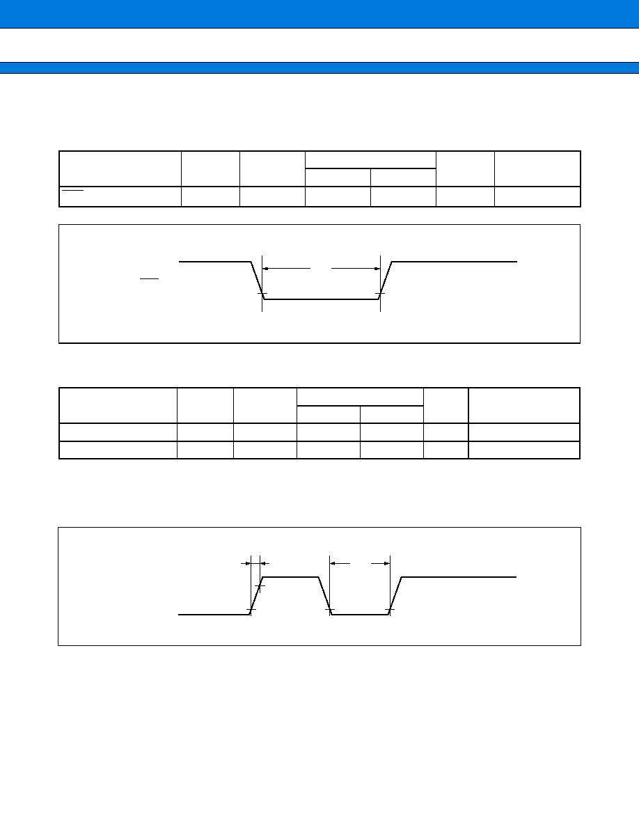
(3) Clock Timings
(AV
SS
=
V
SS
=
0.0 V, T
A
=
-
40
∞
C to
+
85
∞
C)
Parameter
Symbol
Pin Name
Value
Unit
Remarks
Min.
Typ.
Max.
Clock frequency
F
CH
X0, X1
1
10
MHz
Main clock
F
CL
X0A, X1A
32.768
kHz
Sub clock
Clock cycle time
t
HCYL
X0, X1
100
1000
ns
Main clock
t
LCYL
X0A, X1A
30.5
µ
s
Sub clock
Input clock pulse width
P
WH
P
WL
X0
20
ns
External clock
P
WHL
P
WLL
X0A
15.2
µ
s
External clock
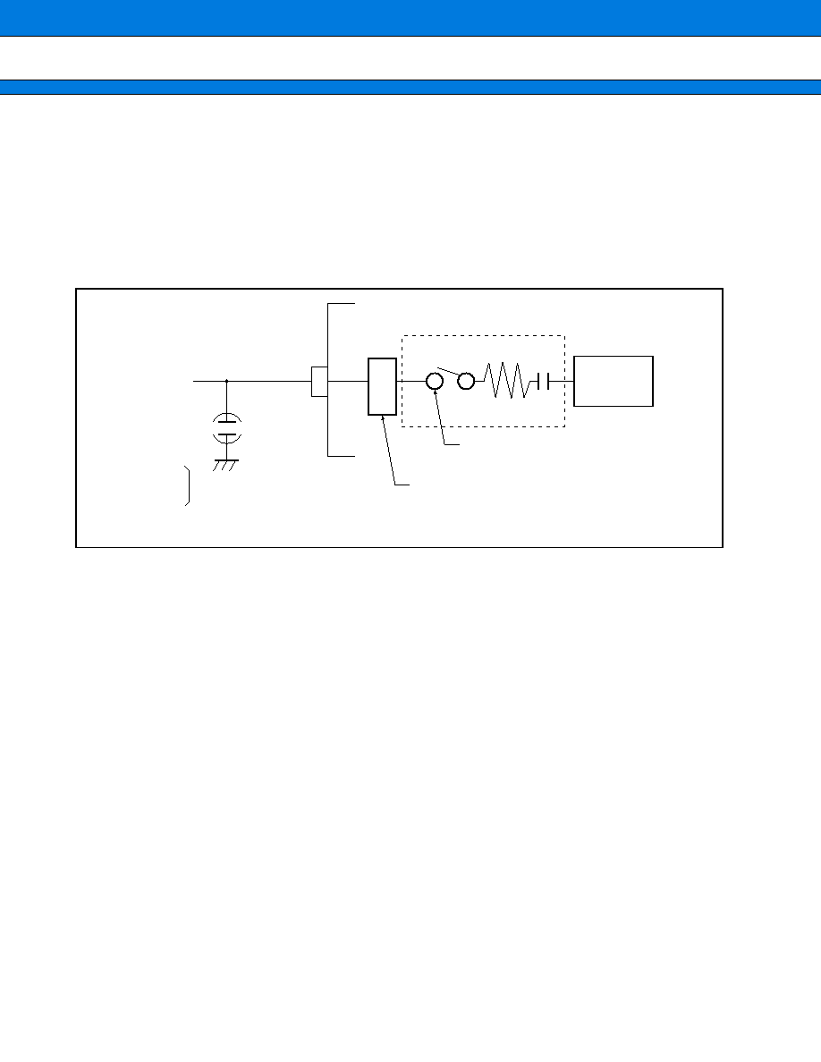
Input clock rising/falling time
t
CR
t
CF
X0
10
ns
External clock
0.2 V
CC
0.2 V
CC
0.8 V
CC
0.8 V
CC
0.2 V
CC
P
WH
t
HCYL
t
CR
t
CF
P
WL
X0
X0
X1
When using
a crystal oscillator
or ceramic oscillator
When using
an external clock
X0
X1
Open circuit
F
CH
C
1
C
2
F
CH
∑
X0 and X1 clock timing and input conditions
∑
Clock configurations

MB89960 Series
33
(4) Instruction Cycle
(AV
SS
=
V
SS
=
0.0 V, T
A
=
-
40
∞
C to
+
85
∞
C)
Parameter
Symbol
Value
Unit
Remarks
Instruction cycle
(Minimum instruction
execution time)
t
INST
4/F
CH
, 8/F
CH
, 16/F
CH
, 64/F
CH
µ
s
F
CH
=
10 MHz (4/F
CH
) operation
time
t
INST
=
0.4
µ
s
2/F
CL
F
CL
=
32.768 kHz operation
time
t
INST
=
61.036
µ
s
0.2 V
CC
0.2 V
CC
0.8 V
CC
0.8 V
CC
0.2 V
CC
P
WHL
t
LCYL
t
CR
t
CF
P
WLL
X0A
X0A
X1A
X0A
X1A
F
CL
C
1
C
2
F
CL
When using
a crystal oscillator
or ceramic oscillator
When using
an external clock
Open circuit
∑
X0A and X1A clock timing conditions
∑
Sub clock configuration
MB89960 Series
34
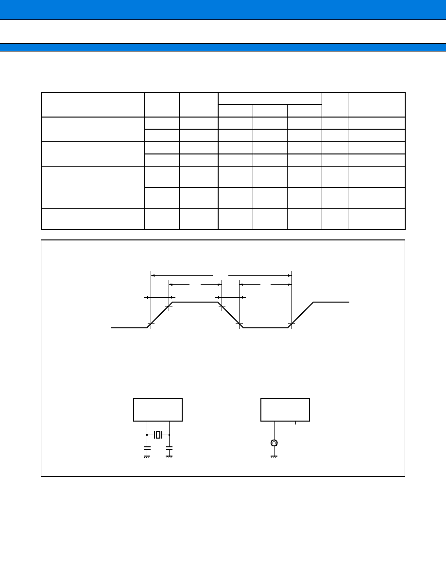
(5) Serial I/O Timings
(V
CC
=
5.0 V, AV
SS
=
V
SS
=
0.0 V, T
A
=
-
40
∞
C to
+
85
∞
C)
* : See " (4) Instruction cycle" for a definition of t
INST
.
Parameter
Sym-
bol
Pin Name
Condition
Value
Unit
Remarks
Min.
Max.
Serial clock cycle time
t
SCYC
SCK
Internal
clock
operation
2 t
INST
*
µ
s
SCK
SO delay time
t
SLOV
SCK, SO
-
200
200
ns
Valid SI
SCK
t
IVSH
SCK, SI
200
ns
SCK
valid SI hold time
t
SHIX
SCK, SI
200
ns
Serial clock "H" pulse width
t
SHSL
SCK
External
clock
operation
t
INST
*
µ
s
Serial clock "L" pulse width
t
SLSH
SCK
t
INST
*
µ
s
SCK
SO delay time
t
SLOV
SCK, SO
0
200
ns
Valid SI
SCK
t
IVSH
SCK, SI
200
µ
s
SCK
valid SI hold time
t
SHIX
SCK, SI
200
µ
s
0.2 V
CC
0.8 V
CC
0.8 V
CC
0.8 V
CC
0.2 V
CC
0.2 V
CC
t
SCYC
t
SLOV
t
IVSH
t
SHIX
SCK
SO
SI
0.2 V
CC
0.8 V
CC
0.2 V
CC
0.2 V
CC
0.2 V
CC
0.8 V
CC
0.8 V
CC
0.8 V
CC
0.8 V
CC
0.2 V
CC
t
SLSH
t
SHSL
t
SLOV
t
IVSH
t
SHIX
SCK
SO
SI
0.2 V
CC
0.8 V
CC
0.2 V
CC
∑
External shift clock mode
∑
Internal shift clock mode

MB89960 Series
35
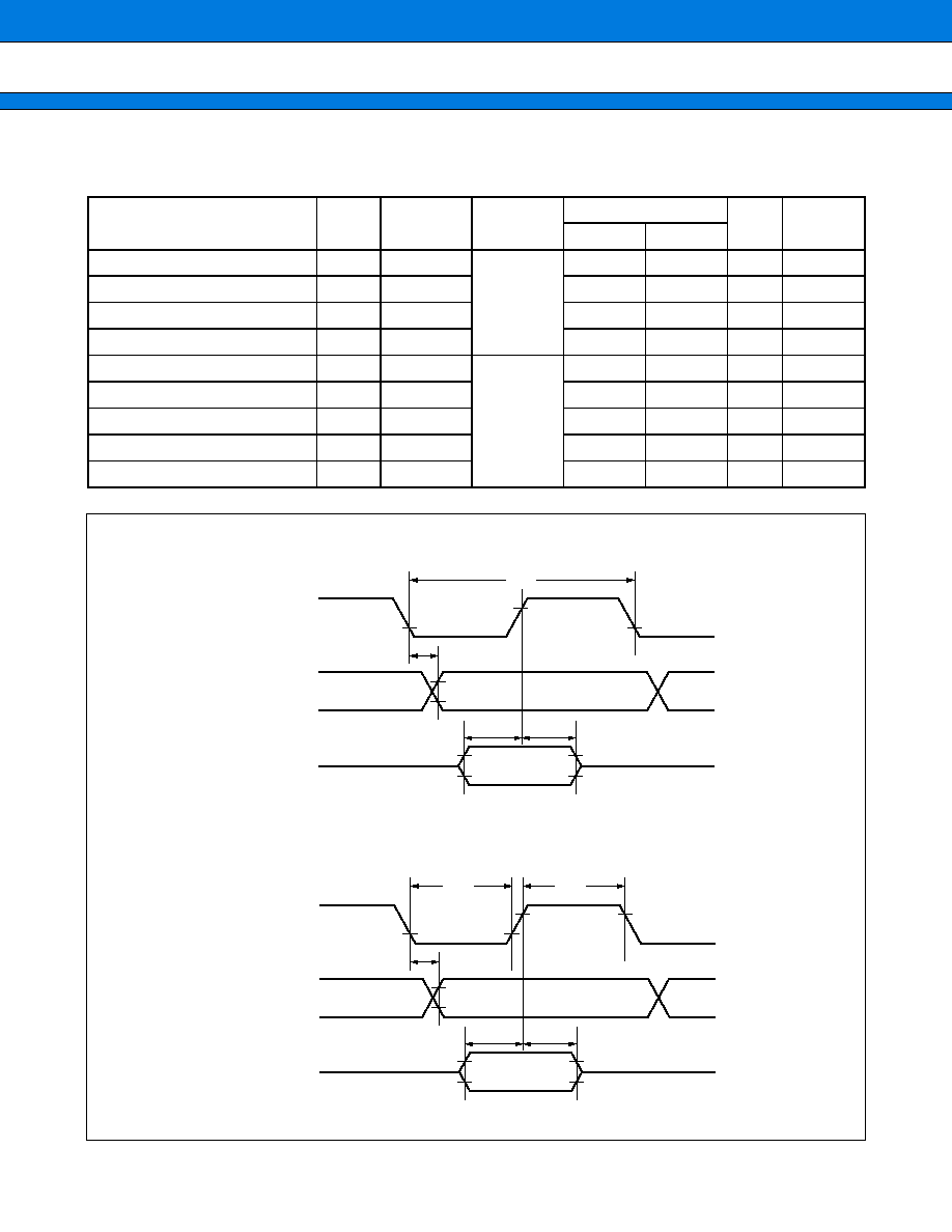
(6) Peripheral Input Timings
(V
CC
=
5.0 V, AV
SS
=
V
SS
=
0.0 V, T
A
=
-
40
∞
C to
+
85
∞
C)
* : See " (4) Instruction cycle" for a definition of t
INST
.
Parameter
Symbol
Pin Name
Value
Unit
Remarks
Min.
Max.
Peripheral input "H" pulse width
t
ILIH
INT10 to INT12,
INT20 to INT27, EC
2 t
INST
*
µ
s
Peripheral input "L" pulse width
t
IHIL
2 t
INST
*
µ
s
0.2 V
CC
0.8 V
CC
0.8 V
CC
0.2 V
CC
t
ILIH
t
IHIL
INT10
INT12,
INT20
INT27, EC

MB89960 Series
36
j
(7) I
2
C Timings
(V
CC
=
5.0 V, AV
SS
=
V
SS
=
0.0 V, T
A
=
-
40
∞
C to
+
85
∞
C)
*1: See " (4) Instruction cycle" for a definition of t
INST
.
*2: m is the value set in the ICCR : CS4 and CS3 bits (bits 4 to 3) .
*3: n is the value set in the ICCR : CS2 to CS0 bits (bits 2 to 0) .
Parameter
Sym
bol
Pin
Value
Unit
Remarks
Min.
Max.
Start condition
output
t
STA
SCL
SDA
1/4t
INST
*
1
◊
m*
◊
n*
3
-
20
1/4t
INST
*
1
◊
m*
2
◊
n*
3
+
20
ns
Master mode
Stop condition
output
t
STO
SCL
SDA
1/4t
INST
*
1
◊
(m*
2
◊
n*
3
+
8)
-
20
1/4t
INST
*
1
◊
(m*
2
◊
n*
3
+
8)
+
20
ns
Master mode
Start condition
detect
t
STA
SCL
SDA
1/4t
INST
*
1
◊
6
+
40
ns
Stop condition
detect
t
STO
SCL
SDA
1/4t
INST
*
1
◊
6
+
40
ns
Restart condition out-
put
t
STASU
SCL
SDA
1/4t
INST
*
1
◊
(m*
2
◊
n*
3
+
8)
-
20
1/4t
INST
*
1
◊
(m*
2
◊
n*
3
+
8)
+
20
ns
Master mode
Restart condition de-
tect
t
STASU
SCL
SDA
1/4t
INST
*
1
◊
4+40
ns
SCL output "L" width
t
LOW
SCL
1/4t
INST
*
1
◊
m*
2
◊
n*
3
-
20
1/4t
INST
*
1
◊
m*
2
◊
n*
3
+
20
ns
Master mode
SCL output "H" width
t
HIGH
SCL
1/4t
INST
*
1
◊
(m*
2
◊
n*
3
+
8)
-
20
1/4t
INST
*
1
◊
(m*
2
◊
n*
3
+
8)
+
20
ns
Master mode
SDA output delay
t
DO
SDA
1/4t
INST
*
1
◊
4
-
20
1/4t
INST
*
1
◊
4
+
20
ns
SDA output setup
time after interrupt
t
DOSU
SDA
1/4t
INST
*
1
◊
4
-
20
ns
SCL input "L" pulse
width
t
LOW
SCL
1/4t
INST
*
1
◊
6
+
40
ns
SCL input "H" pulse
width
t
HIGH
SCL
1/4t
INST
*
1
◊
2
+
40
ns
SDA input setup time
t
SU
SDA
40
ns
SDA hold time
t
HO
SDA
0
ns
SDA
SCL
SDA
SCL
1
6
7
8
9
9
t
DO
t
DO
t
SU
t
SU
t
HIGH
t
LOW
t
HO
t
DO
t
DO
t
DOSU
t
STO
t
HO
t
DOSU
t
STASU
t
STA
t
LOW
t
HO
ACK
ACK
∑ Data transmit (master/slave)
∑ Data receive (master/slave)

MB89960 Series
37
5.
Electrical Characteristics for the A/D Converter
(AVcc
=
3.5 V to 5.5 V, AV
SS
=
V
SS
=
0.0 V, T
A
=
-
40
∞
C to
+
85
∞
C)
*1 : See " (4) Instruction cycle" for a definition of t
INST
.
*2 : Includes sampling time.
Parameter
Sym
bol
Pin
Condition
Value
Unit
Remarks
Min.
Typ.
Max.
Resolution
10
bit
Total error
AVR
=
A
VCC
-
5.0
+
5.0
LSB
Non-linearity error
-
2.5
+
2.5
LSB
Differential
linearity error
-
1.9
+
1.9
LSB
Zero transition voltage
V
OT
AVR
-
3.5
LSB
AVR
+
0.5
LSB
AVR
+
4.5
LSB
mV
Full-scale transition
voltage
V
FST
V
CC
-
6.5
LSB
V
CC
-
1.5
LSB
V
CC
+
1.5
LSB
mV
Variation between
channels
4
LSB
A/D mode conversion
time*
2
60 t
INST
*
1
µ
s
MB89965
MB89P965A
MB89F969A
38 t
INST
*
1
µ
s
MB89PV960
A/D sampling time
16 t
INST
*
1
µ
s
Analog input current
I
AIN
AN0
to
AN3
10
µ
A
Analog input voltage
range
V
AIN
AV
SS
AVR
V
Power supply current
I
A
A
VCC
A/D operation
1.5
3
mA
I
AH
T
A
=
+
25
∞
C
A/D stop
1
5
µ
A
Reference voltage
AVR
AV
SS
+
3.5
AV
CC
V
Reference voltage
supply current
I
R
A/D operation
400
µ
A
I
RH
A/D stop
5
µ
A

MB89960 Series
38
6.
A/D Converter Glossary
∑ Resolution
The change in analog voltage that can be recognized by the A/D converter.
∑ Linearity error (unit : LSB)
The deviation between the actual conversion characteristics and the line linking the zero transition point ("00
0000 0000
B
"
"00 0000 0001
B
") and the full scale transition point ("11 1111 1110
B
"
"11 1111 1111
B
") .
∑ Differential linearity error (unit : LSB)
The variation from the ideal input voltage required to change the output code by 1 LSB.
∑ Total error (unit : LSB)
The total error is the difference between the actual value and the theoretical value.
3FF
H
3FE
H
3FD
H
004
H
003
H
002
H
001
H
AV
SS
AVR
V
OT
0.5 LSB
1 LSB
Theoretical I/O Characteristics
Analog Input
Digital Output
1.5 LSB
V
FST
1 LSB
=
(V)
V
FST
-
V
OT
1022
3FF
H
3FE
H
3FD
H
004
H
003
H
002
H
001
H
AV
SS
AVR
V
NT
{1 LSB
◊
N
+
0.5 LSB}
Actual conversion
characteristic
Actual conversion
characteristic
Theoretical characteristic
Total Error
Analog input
Digital output
V
NT
-
{1 LSB
◊
N
+
0.5 LSB}
1 LSB
Total error for digital output N
=

MB89960 Series
39
004
H
003
H
002
H
001
H
AV
SS
Actual conversion
characteristic
Actual conversion
characteristic
V
OT
(Actual measured value)
Zero Transition Error
Analog Input
Digital Output
3FF
H
3FE
H
3FD
H
3FC
H
AVR
Theoretical characteristic
Actual conversion
characteristic
(Actual
measured value)
Actual conversion
characteristic
Full Scale Transition Error
Analog Input
Digital Output
V
FST
3FF
H
3FE
H
3FD
H
004
H
003
H
002
H
001
H
AV
SS
V
NT
AVR
{1 LSB
◊
N
+
V
OT
}
Actual conversion
characteristic
V
FST
(Actual
measured
value)
Actual conversion
characteristic
Theoretical characteristic
V
OT
(Actual measured value)
Linearity Error
Analog input
Digital output
V
NT
-
{1 LSB
◊
N
+
V
OT
}
1 LSB
Linearity error of digital output N
=
N
+
1
N
N
-
1
N
-
2
AV
SS
AVR
V
NT
Theoretical characteristic
Actual conversion
characteristic
Actual conversion
characteristic
V
(N
+
1) T
Differential Linearity Error
Analog Input
Digital output
Differential linearity error of digital output N
=
-
1
V
(N
+
1) T
-
V
NT
1 LSB
MB89960 Series
40
7.
Notes for A/D Conversion
∑ Analog input pins and input impedance
The A/D converter incorporates a sample & hold circuit as shown below. When an A/D conversion starts, the
voltage at the analog input pin is captured by the sample & hold capacitor for a period of 16 instruction cycles.
Accordingly, if the output impedance of the external circuit connected to the analog input is high, the analog
input voltage may not stabilize within the period of the analog input sampling time. Therefore, ensure that the
output impedance of the external circuit is sufficiently low (10 k
or less) . If it is not possible to reduce the output
impedance of the external circuit, connecting an external capacitor of approximately 0.1
µ
F is recommended.
∑ Error
The relative error increases as |AVR
-
AV
SS
| becomes smaller.
AN0 to AN3
Sample & hold circuit
Comparator
controller
R
Analog channel selector
Closed for approximately 16 instruction cycles
after initiating A/D conversion.
MB89965
MB89P965A
MB89F969A
R
=
3.2 k
, C
=
30 pF approx
R
=
1.4 k
, C
=
64 pF approx.
MB89960 series
MB89PV960
C
Equivalent circuit of analog input

MB89960 Series
41
8.
Electrical Characteristics of Flash Memory
∑ Programming and erasing characteristics
*1 : Automatic algorithm executing
*2 : If a fault occurs during sector erasing, detection via DQ
5
may not be available (DQ
5
=
1 may not occur) .
Accordingly, a fault must be assumed after 15 s, even if DQ
5
does not go to "1".
Parameter
Sym
bol
Pin
Name
Condition
Value
Unit Remarks
Min. Typ. Max.
Power supply current*
1
I
FWE
V
CC
V
CC
=
5.0 V
40
mA
Sector erasing
time
Fixed time
per sector
regardless of
size
Successful
completion
time
1
15
s
Unsuccess-
ful comple-
tion time
*2
Programming
time
per byte
Successful
completion
time
8
3600
µ
s
Unsuccess-
ful comple-
tion time
650 3600
µ
s

MB89960 Series
42
s
s
s
s
MASK OPTIONS
F
CH
: Frequency of main clock oscillation
* : This specifies the initial value after a reset of the oscillation stabilization delay time setting bits in the system
clock control register (SYCC : WT1, WT0)
s
s
s
s
ORDERING INFOMATION
NO
Part No.
MB89965
MB89P965A/
MB89F969A
MB89PV960
Specifying procedure
Specify when
ordering mask
Not available
Not available
1
Initial value* selection for main
clock oscillation stabilization
delay time (F
CH
=
10 MHz)
∑
01 : 2
12
/F
CH
(0.4 ms approx.)
∑
10 : 2
16
/F
CH
(6.6 ms approx.)
∑
11 : 2
18
/F
CH
(26.2 ms approx.)
Selectable
2
18
/F
CH
(26.2 ms approx.)
2
18
/F
CH
(26.2 ms approx.)
Part Number
Package
Remarks
MB89965PFV1
MB89P965APFV1
MB89965CPFV1
Plastic LQFP, 48-pin
(FPT-48P-M05)
The MB89965PFV1 does not have an I
2
C
function.
MB89965PFM
MB89P965APFM
MB89965CPFM
Plastic QFP, 48-pin
(FPT-48P-M13)
The MB89965PFM does not have an I
2
C
function.
MB89965PF
MB89P965APF
MB89965CPF
Plastic QFP, 48-pin
(FPT-48P-M16)
The MB89965PF does not have an I
2
C
function.
MB89F969APFM
Plastic LQFP, 64-pin
(FPT-64P-M09)
MB89PV960CF
Ceramic MQFP, 48-pin
(MQP-48C-P01)

MB89960 Series
43
s
s
s
s
PACKAGE DIMENSIONS
(These package dimensions are provisional. Please obtain the actual dimensions of the final product separately.)
Plastic LQFP, 48-pin
(FPT-48P-M05)
Note : The pin width and thickness includes plating.
Dimensions in mm (inches).
C
2000 FUJITSU LIMITED F48013S-c-4-8
24
13
36
25
48
37
INDEX
7.00±0.10(.276±.004)SQ
9.00±0.20(.354±.008)SQ
0.145±0.055
(.006±.002)
0.08(.003)
"A"
0∞~8∞
.059
≠.004
+.008
≠0.10
+0.20
1.50
0.50±0.20
(.020±.008)
0.60±0.15
(.024±.006)
0.10±0.10
(.004±.004)
(Stand off)
0.25(.010)
Details of "A" part
1
12
0.08(.003)
M
(.008±.002)
0.20±0.05
0.50(.020)
LEAD No.
(Mounting height)

MB89960 Series
44
Plastic QFP, 48-pin
(FPT-48P-M13)
Dimensions in mm (inches).
C
2000 FUJITSU LIMITED F48023S-1C-2
Details of "A" part
13.10±0.40
0.30±0.10
(.012±.004)
0.16(.006)
M
11.50±0.30
8.80
(.453±.012)
(.346)
REF
INDEX
Details of "B" part
12
1
25
36
37
24
13
48
0.80(.0315)TYP
LEAD No.
(.516±.016)
SQ
(.394±.008)
10.00±0.20 SQ
"A"
0.15±0.05
(.006±.002)
0.15(.006)
0.20(.008)
0.53(.021)MAX
0.18(.007)MAX
0~10∞
0.80±0.30
(.031±.012)
"B"
(STAND OFF)
0(0)MIN
2.35(.093)MAX
(Mounting height)
0.10(.004)

MB89960 Series
45
Plastic QFP, 48-pin
(FPT-48P-M16)
Dimensions in mm (inches).
C
2000 FUJITSU LIMITED F48026S-1C-2
Details of "A" part
17.20±0.40
0.30±0.06
(.012±.002)
0.16(.006)
M
13.60±0.40
8.80
(.535±.016)
(.346)
REF
0.15(.006)
INDEX
Details of "B" part
12
1
25
36
37
24
13
48
0.80(.0315)TYP
LEAD No.
(.677±.016)
SQ
SQ
"A"
0.15(.006)
0.20(.008)
0.50(.020)MAX
0.15(.006)MAX
0~10∞
1.80±0.30
(.071±.012)
"B"
(STAND OFF)
0.05(.002)MIN
.472
≠.004
+.012
≠0.10
+0.30
12.00
.006
≠.0004
+.002
≠0.01
+0.05
0.15
2.70(.106)MAX
(Mounting height)
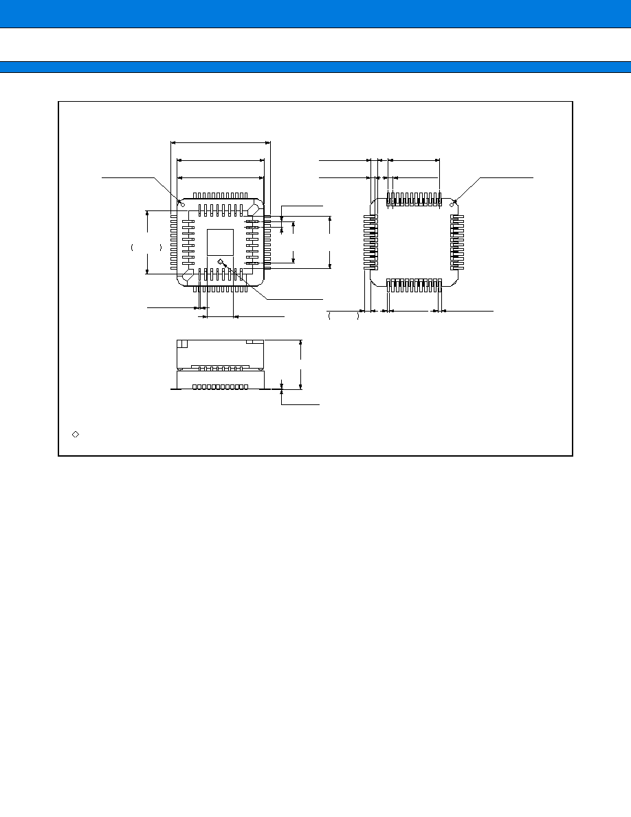
MB89960 Series
46
Ceramic MQFP, 48-pin
(MQP-48C-P01)
Dimensions in mm (inches).
≠.010
+.018
≠0.25
+0.45
+0.13
≠0.0
+.005
≠0
PIN No.1 INDEX
1.50(.059)TYP
1.00(.040)TYP
8.80(.346)REF
(.0315±.0087)
0.80±0.22
(.016±.003)
0.40±0.08
.043
1.10
0.60(.024)TYP
8.50(.335)MAX
(.006±.002)
0.15±0.05
PAD No.1 INDEX
4.50(.177)TYP
0.30(.012)TYP
TYP
TYP
8.71(.343)
7.14(.281)
(.040±.005)
1.02±0.13
10.92
.430
PIN No.1 INDEX
17.20(.677)TYP
(.591±.010)
15.00±0.25
(.583±.014)
14.82±0.35
1994 FUJITSU LIMITED M48001SC-4-2
C
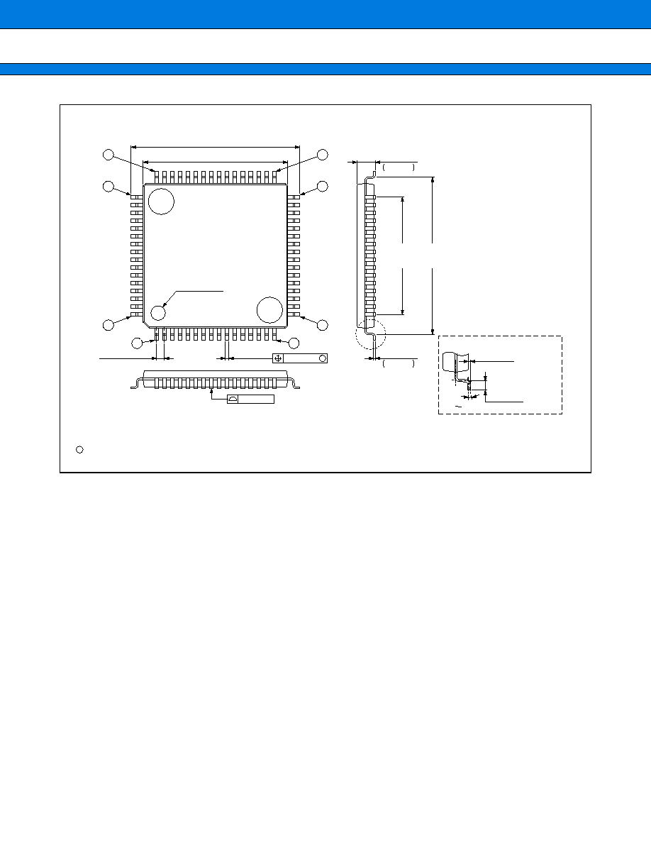
MB89960 Series
47
Plastic LQFP, 64-pin
(FPT-64P-M09)
Dimensions in mm (inches).
C
2000 FUJITSU LIMITED F64018S-1C-3
0.13(.005)
M
1 PIN INDEX
.005
≠.001
+.002
≠0.02
+0.05
0.127
.059
≠.004
+.008
≠0.10
+0.20
1.50
"A"
Details of "A" part
0 10∞
0.50±0.20
0.10±0.10
(.004±.004)
(.020±.008)
14.00±0.20(.551±.008)SQ
12.00±0.10(.472±.004)SQ
0.65(.0256)TYP
0.30±0.10
(.012±.004)
9.75
13.00
(.384)
REF
(.512)
NOM
1
16
17
32
33
48
49
64
(STAND OFF)
LEAD No.
(Mounting height)
0.10(.004)

MB89960 Series
FUJITSU LIMITED
All Rights Reserved.
The contents of this document are subject to change without notice.
Customers are advised to consult with FUJITSU sales
representatives before ordering.
The information and circuit diagrams in this document are
presented as examples of semiconductor device applications, and
are not intended to be incorporated in devices for actual use. Also,
FUJITSU is unable to assume responsibility for infringement of
any patent rights or other rights of third parties arising from the use
of this information or circuit diagrams.
The products described in this document are designed, developed
and manufactured as contemplated for general use, including
without limitation, ordinary industrial use, general office use,
personal use, and household use, but are not designed, developed
and manufactured as contemplated (1) for use accompanying fatal
risks or dangers that, unless extremely high safety is secured, could
have a serious effect to the public, and could lead directly to death,
personal injury, severe physical damage or other loss (i.e., nuclear
reaction control in nuclear facility, aircraft flight control, air traffic
control, mass transport control, medical life support system, missile
launch control in weapon system), or (2) for use requiring
extremely high reliability (i.e., submersible repeater and artificial
satellite).
Please note that Fujitsu will not be liable against you and/or any
third party for any claims or damages arising in connection with
above-mentioned uses of the products.
Any semiconductor devices have an inherent chance of failure. You
must protect against injury, damage or loss from such failures by
incorporating safety design measures into your facility and
equipment such as redundancy, fire protection, and prevention of
over-current levels and other abnormal operating conditions.
If any products described in this document represent goods or
technologies subject to certain restrictions on export under the
Foreign Exchange and Foreign Trade Law of Japan, the prior
authorization by Japanese government will be required for export
of those products from Japan.
F0104
©
FUJITSU LIMITED Printed in Japan