 | –≠–ª–µ–∫—Ç—Ä–æ–Ω–Ω—ã–π –∫–æ–º–ø–æ–Ω–µ–Ω—Ç: MB40C568H | –°–∫–∞—á–∞—Ç—å:  PDF PDF  ZIP ZIP |
DS04-28207-2E
FUJITSU SEMICONDUCTOR
DATA SHEET
ASSP for Image Processing
CMOS
A/D Converter
(1-channel, 8-bit, 20MHz)
MB40C568
s
DESCRIPTION
The MB40C568 is a high-speed A/D converter using high-speed CMOS process technology.
s
FEATURES
∑ Resolution: 8 bits
∑ Linearity error:
±
0.20% (Typ.)
∑ Maximum conversion rate: 20 MSPS (Min.)
∑ Power supply voltage: Analog section +5.0 V
Digital section +3.0 V or +5.0 V
∑ Digital input voltage range: TTL level
∑ Digital output voltage range: CMOS level compatible
∑ Analog input voltage range: 0.5 to 4 V (with 2 Vp-p)
∑ Analog input capacity: 15 pF (Typ.)
∑ Power consumption: 50 mW (Typical:@f
CLK
= 20 MHz, AV
DD
= 5 V, DV
DD
= 3 V)
60 mW (Typical:@f
CLK
= 20 MHz, AV
DD
= DV
DD
= 5 V)
∑ Additional function: Reference voltage generator circuit: V
REFT
= 3 V, V
REFB
= 1 V
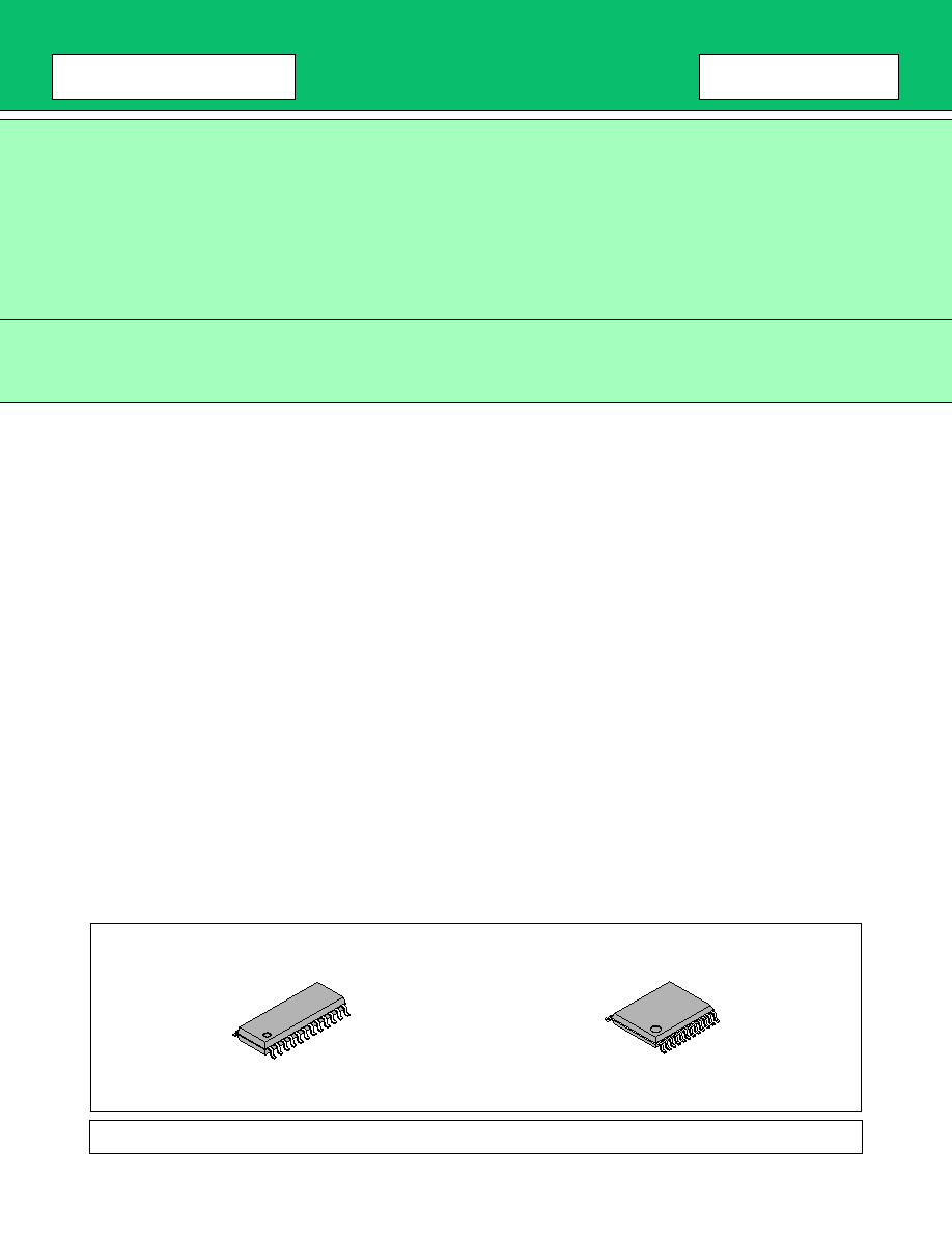
∑ Package options: SOP24, SSOP24
s
PACKAGES
This device contains circuitry to protect the inputs against damage due to high static voltages or electric fields. However, it is advised that normal precautions
be taken to avoid application of any voltage higher than maximum rated voltages to this high impedance circuit.
(FPT-24P-M03)
(FPT-24P-M01)
24-pin, Plastic SOP
24-pin, Plastic SSOP
2
MB40C568
s
PIN ASSIGNMENT
s
PIN DESCRIPTION
Values within ( ) are typical values.
s
NOTES ON USE
∑ Be sure to bypass the AV
DD
, DV
DD
, V
RT
and V
RB
pins to the ground using a high-frequency capacitor.
The high-frequency capacitor should be connected as near the pin as possible.
∑ Provide four clocks or more immediately after the power up to prevent current dissipation due to the
indeterminate internal logic.
Pin No.
Pin name
Functions
1, 18
AV
DD
Analog power supply pins (+5 V)
2, 13, 16
DV
DD
Digital power supply pins (+3 or +5 V)
3, 15, 17, 24
AV
SS
Analog power ground pins (0 V)
12
DV
SS
Digital power ground pin (0 V)
4 to 11
D
1
to D
8
Digital output pins. D
1
: MSB, D
8
: LSB
14
CLK
Clock input pin
21
V
INA
Analog input pin. Input range: V
RB
to V
RT
(2 Vp-p between 0.5 to 4 V)
19
V
RT
Reference voltage input pin (3 V)
20
V
REFT
Reference voltage output pin. When connected to V
RT
, the pin generates
0.6
◊
AV
DD
(3 V).
23
V
RB
Reference voltage input pin (1 V)
22
V
REFB
Reference voltage output pin. When connected to V
RB
, the pin generates
0.2
◊
AV
DD
(1 V).
(FPT-24P-M01)
1
2
3
4
5
6
22
21
20
19
18
17
7
8
9
10
16
15
14
13
(TOP VIEW
)
11
12
24
23
AV
DD
DV
DD
AV
SS
(LSB) D
8
D
7
D
6
D
5
D
4
D
3
D
2
(MSB) D
1
DV
SS
AV
SS
V
RB
V
REFB
V
INA
V
REFT
V
RT
AV
DD
AV
SS
DV
DD
AV
SS
CLK
DV
DD
(FPT-24P-M03)
3
MB40C568
s
ABSOLUTE MAXIMUM RATINGS (See WARNING)
WARNING: Semiconductor devices can be permanently damaged by application of stress (voltage, current,
temperature, etc.) in excess of absolute maximum ratings. Do not exceed these ratings.
s
RECOMMENDED OPERATING CONDITIONS
WARNING: Recommended operating conditions are normal operating ranges for the semiconductor device. All
the device's electrical characteristics are warranted when operated within these ranges.
Always use semiconductor devices within the recommended operating conditions. Operation outside
these ranges may adversely affect reliability and could result in device failure.
No warranty is made with respect to uses, operating conditions, or combinations not represented on
the data sheet. Users considering application outside the listed conditions are advised to contact their
FUJITSU representative beforehand.
(Continued)
Parameter
Symbol
Rating
Unit
Min.
Max.
Power supply voltage
AV
DD,
DV
DD
≠0.3
7.0
V
Input voltage
CLK, V
INA
V
RT,
V
RB
≠0.3
AV
DD
+0.3
V
Output voltage
D
1
to D
8
≠0.3
DV
DD
+0.3
V
Storage temperature
Tstg
≠55
+125
∞
C
Parameter
Symbol
Value
Unit
Min. Typ.
Max.
Analog input voltage
V
INA
V
RB
≠
V
RT
V
Analog reference voltage: T
V
RT
≠
≠
4.00
V
Analog reference voltage: B
V
RB
0.50
≠
≠
V
Analog reference voltage range
V
RT
≠V
RB
1.90
2.00
2.10
V
Digital "H" level input voltage
V
IHD
2.4
≠
≠
V
Digital "L" level input voltage
V
ILD
≠
≠
0.8
V
Digital input current
I
ID
≠
≠
5
µ
A
Clock frequency
f
CLK
0.1
≠
20
MHz
Minimum "H" level clock pulse width
tw
+
22.5
≠
≠
ns
Minimum "L" level clock pulse width
tw
≠
22.5
≠
≠
ns
Operating temperature range
Ta
≠20
≠
70
∞
C
4
MB40C568
(Continued)
∑ When using a single power supply
∑ When using dual power supplies
WARNING: Recommended operating conditions are normal operating ranges for the semiconductor device. All
the device's electrical characteristics are warranted when operated within these ranges.
Always use semiconductor devices within the recommended operating conditions. Operation outside
these ranges may adversely affect reliability and could result in device failure.
No warranty is made with respect to uses, operating conditions, or combinations not represented on
the data sheet. Users considering application outside the listed conditions are advised to contact their
FUJITSU representative beforehand.
Parameter
Symbol
Value
Unit
Min. Typ.
Max.
Power supply voltage
AV
DD,
DV
DD
4.75
5.00
5.25
V
Parameter
Symbol
Value
Unit
Min. Typ.
Max.
Power supply voltage
AV
DD
4.75
5.00
5.25
V
DV
DD
2.70
3.00
3.30
V
5
MB40C568
s
ELECTRICAL CHARACTERISTICS (Using a Single Power Supply)
DC Characteristics
(1) Analog section
(AV
DD
= DV
DD
= 4.75 V to +5.25 V, Ta = ≠20
∞
C to +70
∞
C)
(2) Digital section
(AV
DD
= DV
DD
= 4.75 V to +5.25 V, Ta = ≠20
∞
C to +70
∞
C)
(3) Switching section
(AV
DD
= DV
DD
= 4.75 V to +5.25 V, Ta = ≠20
∞
C to +70
∞
C)
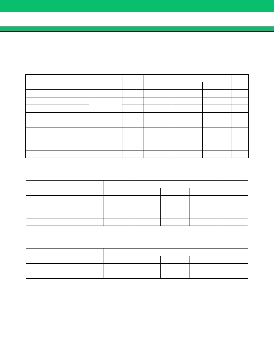
Parameter
Symbol
Value
Unit
Min.
Typ.
Max.
Resolution
≠
≠
8
≠
bit
Linearity error
DC precision
LE
≠
±
0.20
±
0.30
%
Differential linearity error
DLE
≠
±
0.12
±
0.20
%
Analog input capacity
C
INA
≠
15
≠
pF
Reference voltage: T
V
REFT
≠
0.6
◊
AV
DD
≠
V
Reference voltage: B
V
REFB
≠
0.2
◊
AV
DD
≠
V
Reference current
I
RB
≠16.0
≠8.0
≠2.0
mA
Analog power supply current
AI
DD
≠
8.0
14.0
mA
Digital power supply current
DI
DD
≠
4.0
7.0
mA
Parameter
Symbol
Value
Unit
Min. Typ.
Max.
Digital "H" level output voltage
V
OHD
4.2
≠
DV
DD
V
Digital "L" level output voltage
V
OLD
≠
≠
0.4
V
Digital "H" level output current
I
OH
≠400
≠
≠
µ
A
Digital "L" level output current
I
OL
≠
≠
1.6
mA
Parameter
Symbol
Value
Unit
Min. Typ.
Max.
Maximum conversion rate
fs
20
≠
≠
MSPS
Digital output delay time
tpd
0
5
20
ns