FIND Vol.17 No.3

FIND
,
Vol. 17, No. 3, August 1999
N E W
P R O D U C T S
·
M B 8 1 x x 6 4 3 2 4 2 B
·
·
·
·
·
·
·
·
·
·
·
·
·
·
·
·
·
·
·
·
·
·
·
·
·
·
·
·
·
·
·
·
·
·
·
·
·
·
·
·
·
·
·
·
·
·
·
·
·
·
·
·
·
·
·
·
·
·
·
·
·
·
·
·
·
·
·
·
·
·
·
·
·
·
·
·
·
·
·
·
·
·
·
·
·
·
·
·
·
·
·
·
·
·
·
·
·
·
·
·
·
·
·
·
·
·
·
·
·
·
·
·
·
·
·
·
·
·
·
·
·
·
·
·
·
·
·
·
·
·
·
·
·
·
·
·
·
·
·
·
·
·
·
·
·
·
·
·
·
·
·
·
·
·
·
·
·
·
·
·
·
·
·
·
·
·
·
·
·
·
·
·
·
·
·
·
·
·
·
·
·
·
·
·
·
·
·
·
·
·
·
·
·
·
·
·
·
·
·
·
·
·
·
·
·
·
·
·
·
·
·
·
·
·
·
·
·
·
·
·
·
·
·
·
·
·
·
·
·
·
·
·
·
·
·
·
·
·
·
·
·
·
·
2M x 32-Bit
Synchronous DRAM for
Multimedia
&
Graphics:
MB81F643242B
MB811L643242B
The SDRAMs in a 32-bit I/O configuration can provide the effective
solution for a wide range of applications, including multimedia and
graphics applications. Also, these SDRAMs employ the new SCITT
technology, thereby reducing the test time and cost.
Features
·
64 M-bit SDRAM with a 32-bit I/O
configuration
·
High performance series or low power
consumption series
·
Introduction of a new test technology,
SCITT
·
Reduced test time and cost using SCITT
·
Also available as extended operating-
temperature components
·
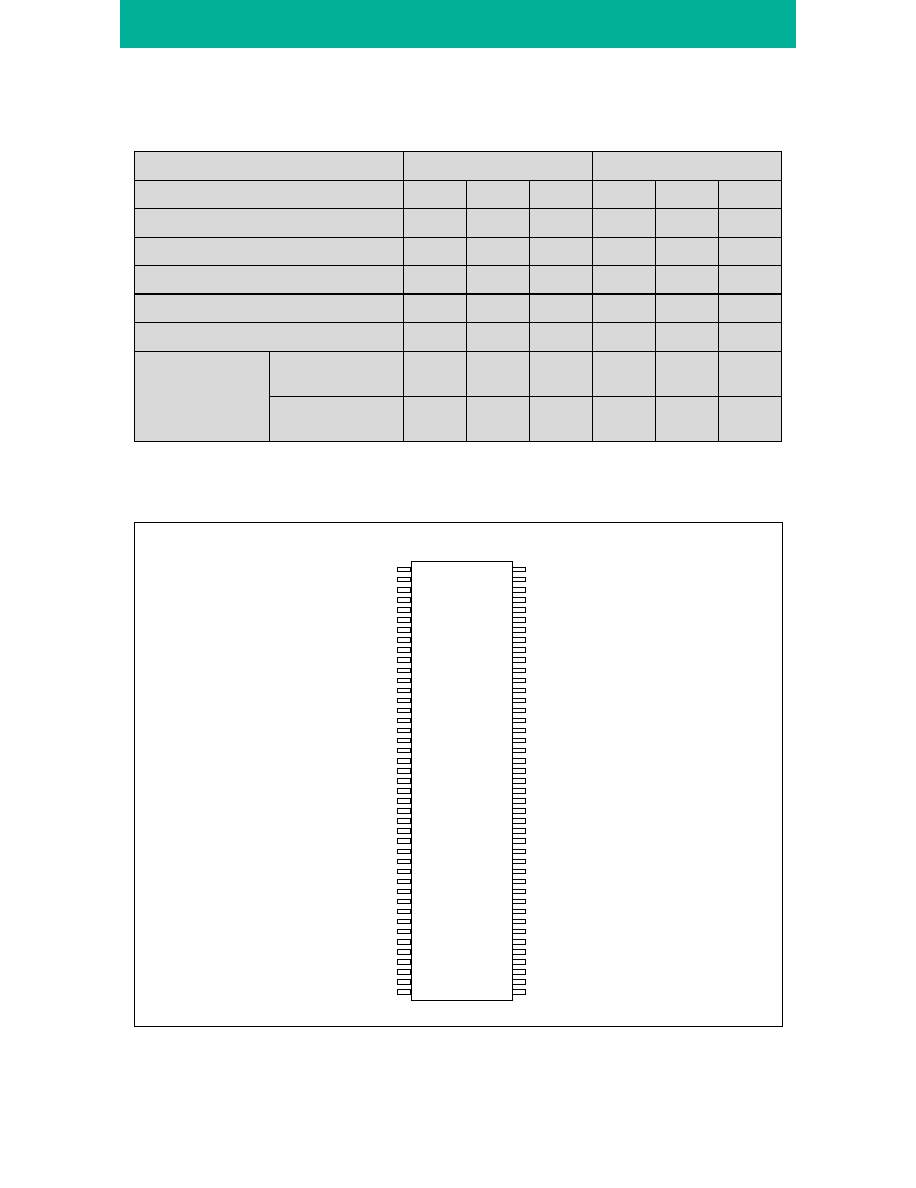
JEDEC Standard 86-pin TSOP package
Photo 1.
MB81xx643242B Appearance
17-3-b2.fm Page 31 Saturday, August 28, 1999 9:57 PM

FIND
,
Vol. 17, No. 3, August 1999
N E W
P R O D U C T S
·
M B 8 1 x x 6 4 3 2 4 2 B
·
·
·
·
·
·
·
·
·
·
·
·
·
·
·
·
·
·
·
·
·
·
·
·
·
·
·
·
·
·
·
·
·
·
·
·
·
·
·
·
·
·
·
·
·
·
·
·
·
·
·
·
·
·
·
·
·
·
·
·
·
·
·
·
·
·
·
·
·
·
·
·
·
·
·
·
·
·
·
·
·
·
·
·
·
·
·
·
·
·
·
·
·
·
·
·
·
·
·
·
·
·
·
·
·
·
·
·
·
·
·
·
·
·
·
·
·
·
·
·
·
·
·
·
·
·
·
·
·
·
·
·
·
·
·
·
·
·
·
·
·
·
·
·
·
·
·
·
·
·
·
·
·
·
·
·
·
·
·
·
·
·
·
·
·
·
·
·
·
·
·
·
·
·
·
·
·
·
·
·
·
·
·
·
·
·
·
·
·
·
·
·
·
·
·
·
·
·
·
·
·
·
·
·
·
·
·
·
·
·
·
·
·
·
·
·
·
·
·
·
·
·
·
·
·
·
·
·
·
·
·
·
·
·
·
·
·
·
·
·
·
·
·
Overview
Synchronous DRAMs (SDRAMs) have been rapidly
increasing in popularity since they were employed
as main memory for personal computers. They have
also been used not only for computer main memory,
but also for various other applications, including
communications equipment, consumer products,
multimedia, graphics, and mobile products. It is ex-
pected that the 64 M-bit SDRAM with a 32-bit I/O
configuration will be adopted as the preferred con-
figuration for many of these applications.
FUJITSU has now developed two series of SDRAM
with a 32-bit I/O configuration:
·
The MB81F643242B is a high-performance
version, operating at a maximum frequency of
143 MHz. This SDRAM is the second-
generation product, based on the current
mass-production 2M x 32-bit SDRAM.
·
The MB811L643242B is a low-voltage, low
power consumption version operating at 2.5V.
These products employ a new test technology, Stat-
ic Component Interconnection Test Technology
(SCITT), developed by a
FUJITSU/Philips (Nether-
lands) collaboration. SCITT
is a new XNOR circuit-
based technology that is
used for board-level inter-
connection testing. Using SCITT's simple method
reduces the test time and cost required for board-
level interconnection testing.
Product Features
The MB81F643242B and MB811L643242B are
SDRAMs in a "4 banks x 512K words x 32 bits" con-
figuration, operating at supply voltages of 3.3V and
2.5V, respectively. These SDRAMs support the fol-
lowing settings:
·
CAS latency: 2 or 3
·
Burst length: 1, 2, 4, 8, or full page
·
Burst type: Sequential or interleave
The package is an 86-pin TSOP with a pin pitch of
0.5 mm, fully conforming to JEDEC standards. The
MB81F643242B Series consists of three speed ver-
sions: 143-MHz, 125-MHz, and 100-MHz. The
MB811L643242B also consists of three speed ver-
sions: 100-MHz, 84-MHz, and 67-MHz. Also, a low
power version is available.
FUJITSU also provides support for the SCITT functions
and for optional, extended operating-temperature
products for use in special environments.
Examples of applications for these SDRAMs are:
·
High-speed model: Graphics card, digital TV,
game equipment, etc.
·
Low-voltage model: Portable video camera,
digital camera, PDA, mobile computer,
consumer product built-in device, etc.
·
Extended operating-temperature models:
Automotive equipment, such as a car
navigation system, application-specific
products, etc.
·
Other applications: Copier, communications
equipment, etc.
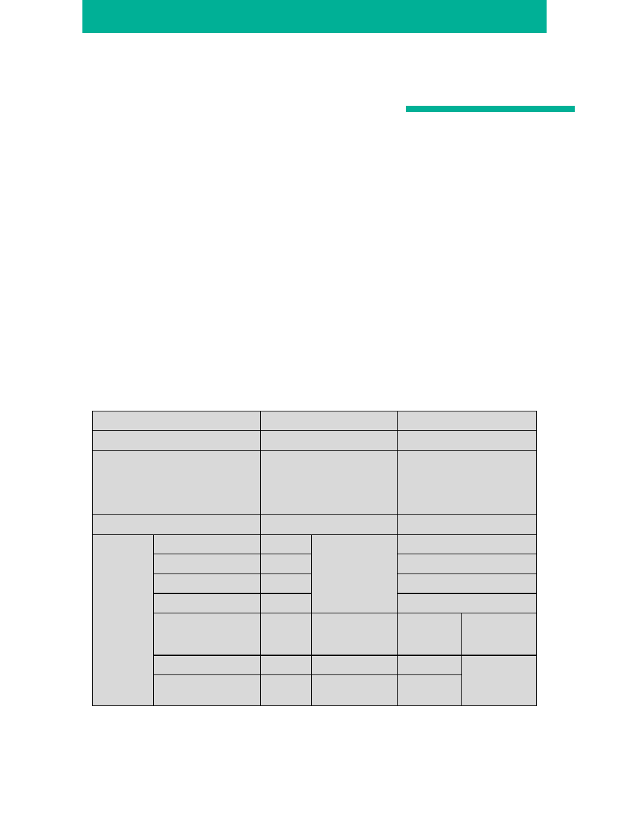
Table 1 lists the major characteristics of these
SDRAMs and Figure 1 shows their pin assignments.
". . . reduces the test time and
cost required for board-level
interconnection testing."
17-3-b2.fm Page 32 Saturday, August 28, 1999 9:57 PM
FIND
,
Vol. 17, No. 3, August 1999
N E W
P R O D U C T S
·
M B 8 1 x x 6 4 3 2 4 2 B
·
·
·
·
·
·
·
·
·
·
·
·
·
·
·
·
·
·
·
·
·
·
·
·
·
·
·
·
·
·
·
·
·
·
·
·
·
·
·
·
·
·
·
·
·
·
·
·
·
·
·
·
·
·
·
·
·
·
·
·
·
·
·
·
·
·
·
·
·
·
·
·
·
·
·
·
·
·
·
·
·
·
·
·
·
·
·
·
·
·
·
·
·
·
·
·
·
·
·
·
·
·
·
·
·
·
·
·
·
·
·
·
·
·
·
·
·
·
·
·
·
·
·
·
·
·
·
·
·
·
·
·
·
·
·
·
·
·
·
·
·
·
·
·
·
·
·
·
·
·
·
·
·
·
·
·
·
·
·
·
·
·
·
·
·
·
·
·
·
·
·
·
·
·
·
·
·
·
·
·
·
·
·
·
·
·
·
·
·
·
·
·
·
·
·
·
·
·
·
·
·
·
·
·
·
·
·
·
·
·
·
·
·
·
·
·
·
·
·
·
·
·
·
·
·
·
·
·
·
·
·
·
·
·
·
·
·
·
·
·
·
·
·
Figure 1.
MB81F643242B/MB811L643242B Pin Assignments
Table 1.
MB81F643242B/MB811L643242B Major Characteristics
Part Number
MB81F643232B
MB811L643242B
Speed Version
70/70L
80/80L
10/10L
10/10L
12/12L
15/15L
Clock Frequency
MHz
143
125
100
100
84
67
Clock Cycle Time
t
CK
(min.)
ns
7
8
10
10
12
15
RAS Cycle Time
t
RC
(min.)
ns
63
72
90
90
100
110
RAS-CAS Delay Time t
RCD
(min.)
ns
21
24
30
30
30
30
RAS Precharge Time
t
RP
(min.)
ns
17
20
30
30
35
40
Clock Access Time
tAC
(CL=2)
ns
6
6
7
8
8
8
tAC
(CL=3)
ns
6
6
7
8
8
8
1
2
3
4
5
6
7
8
9
10
11
12
13
14
15
16
17
18
19
20
21
22
23
24
25
26
27
28
29
30
31
32
33
34
35
36
37
38
39
40
41
42
43
V
CC
DQ
0
V
CCQ
DQ
1
DQ
2
V
SSQ
DQ
3
DQ
4
V
CCQ
DQ
5
DQ
6
V
SSQ
DQ
7
NC
V
CC
DQM
0
/WE
/CAS
/RAS
/CS
NC
A
12
A
11
A
10
/AP
A
0
A
1
A
2
DQM
2
V
CC
NC
DQ
16
V
SSQ
DQ
17
DQ
18
V
CCQ
DQ
19
DQ
20
V
SSQ
DQ
21
DQ
22
V
CCQ
DQ
23
V
CC
V
SS
DQ
15
V
SSQ
DQ
14
DQ
13
V
CCQ
DQ
12
DQ
11
V
SSQ
DQ
10
DQ
9
V
CCQ
DQ
8
NC
V
SS
DQM
1
NC
NC
CLK
CKE
A
9
A
8
A
7
A
6
A
5
A
4
A
3
DQM
3
V
SS
NC
DQ
31
V
CCQ
DQ
30
DQ
29
V
SSQ
DQ
28
DQ
27
V
CCQ
DQ
26
DQ
25
V
SSQ
DQ
24
V
SS
86
85
84
83
82
81
80
79
78
77
76
75
74
73
72
71
70
69
68
67
66
65
64
63
62
61
60
59
58
57
56
55
54
53
52
51
50
49
48
47
46
45
44
Pin No.
Pin No.
Pin Symbol
Pin Symbol
Top View
400 mil x 875 mil
86-Pin TSOP
Pin Pitch
= 0.5 mm
Low Addresses:
A
0
to A
10
Bank Addresses:
A
11
, A
12
Column Addresses:
A
0
to A
7
Auto-Precharge:
A
10
spacer
17-3-b2.fm Page 33 Saturday, August 28, 1999 9:57 PM
FIND
,
Vol. 17, No. 3, August 1999
N E W
P R O D U C T S
·
M B 8 1 x x 6 4 3 2 4 2 B
·
·
·
·
·
·
·
·
·
·
·
·
·
·
·
·
·
·
·
·
·
·
·
·
·
·
·
·
·
·
·
·
·
·
·
·
·
·
·
·
·
·
·
·
·
·
·
·
·
·
·
·
·
·
·
·
·
·
·
·
·
·
·
·
·
·
·
·
·
·
·
·
·
·
·
·
·
·
·
·
·
·
·
·
·
·
·
·
·
·
·
·
·
·
·
·
·
·
·
·
·
·
·
·
·
·
·
·
·
·
·
·
·
·
·
·
·
·
·
·
·
·
·
·
·
·
·
·
·
·
·
·
·
·
·
·
·
·
·
·
·
·
·
·
·
·
·
·
·
·
·
·
·
·
·
·
·
·
·
·
·
·
·
·
·
·
·
·
·
·
·
·
·
·
·
·
·
·
·
·
·
·
·
·
·
·
·
·
·
·
·
·
·
·
·
·
·
·
·
·
·
·
·
·
·
·
·
·
·
·
·
·
·
·
·
·
·
·
·
·
·
·
·
·
·
·
·
·
·
·
·
·
·
·
·
·
·
·
·
·
·
·
·
Photo 2.
MB81xx643242B Chip
SCITT Functions
Most of the failures occurring after mounting LSIs on
the board are attributable to open-circuit, mounting,
or short-circuit faults. In addition, new packaging
technologies make the post-mounting test more
complicated. Considering these factors, FUJITSU,
in collaboration with Philips, planned and developed
the method for simply testing the mutual connection
between LSIs mounted on the board.
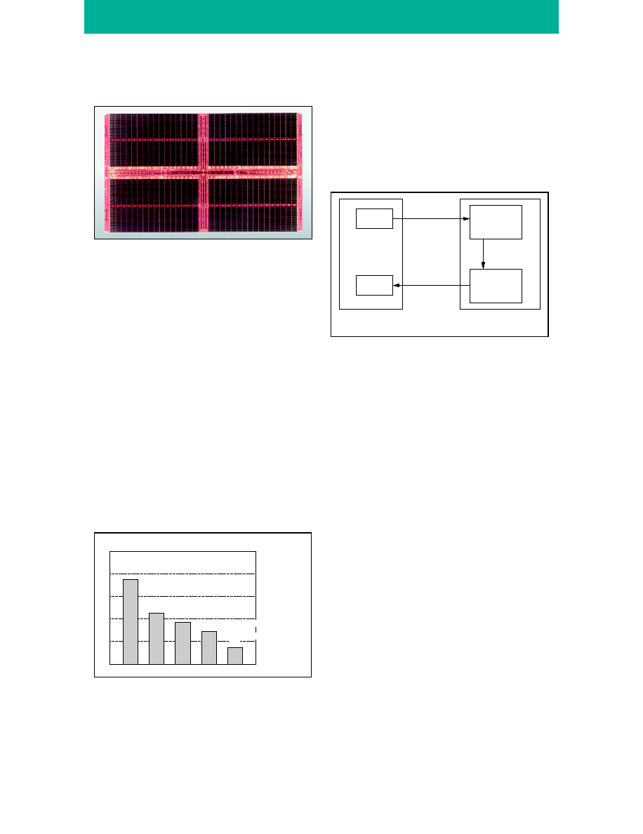
Figure 2 shows post-mounting fault ratios. Figure 3
illustrates the basic concept of SCITT technology,
developed for detecting connection faults.
Figure 2. Post-Mounting Fault Ratios
The host controller outputs a test pattern on the ad-
dress and control pins to memory. This test pattern
had been stored in ROM in the host controller during
controller design. The memory outputs a correspond-
ing test pattern to the host controller via the I/O pins.
The host side then checks the output pattern from the
memory and compares the expected value and actu-
al output value to detect open-circuit faults, short-
circuit faults, missing LSIs, and mounting errors.
Figure 3. SCITT Technology Basic Concept
SCITT Advantages
The following features of SCITT can be listed as its
advantages over the boundary scan method.
·
No need for dedicated pins
·
Short test time: 1/1,000 of the current test
time or less
·
Fault reject ratio: almost 100%
·
Insignificant increase in chip size
Table 2 compares the interconnection tests by the
SCITT and boundary scan methods.
SCITT Specifications for SDRAM
The SDRAM with SCITT functions has the following
SCITT specifications.
Figure 4 shows the state diagram of SCITT mode. As
shown in the figure, the SCITT functions are execut-
ed only before initialization after the supply voltage
is applied. The SCITT functions are optional; the ex-
ecution is not required.
50
40
30
20
10
0
37%
22%
19%
14%
Open-Circuit Failure
Mounting Failure
Analog Failure
7%
(%)
LSI Function Failure
Short-Circuit Failure
ROM
ROM &
Decoder
Output
Buffer
Evaluation
Memory
Controller
Memory
x Address
Data Bus
x Address: Address + Control Line
17-3-b2.fm Page 34 Saturday, August 28, 1999 9:57 PM
FIND
,
Vol. 17, No. 3, August 1999
N E W
P R O D U C T S
·
M B 8 1 x x 6 4 3 2 4 2 B
·
·
·
·
·
·
·
·
·
·
·
·
·
·
·
·
·
·
·
·
·
·
·
·
·
·
·
·
·
·
·
·
·
·
·
·
·
·
·
·
·
·
·
·
·
·
·
·
·
·
·
·
·
·
·
·
·
·
·
·
·
·
·
·
·
·
·
·
·
·
·
·
·
·
·
·
·
·
·
·
·
·
·
·
·
·
·
·
·
·
·
·
·
·
·
·
·
·
·
·
·
·
·
·
·
·
·
·
·
·
·
·
·
·
·
·
·
·
·
·
·
·
·
·
·
·
·
·
·
·
·
·
·
·
·
·
·
·
·
·
·
·
·
·
·
·
·
·
·
·
·
·
·
·
·
·
·
·
·
·
·
·
·
·
·
·
·
·
·
·
·
·
·
·
·
·
·
·
·
·
·
·
·
·
·
·
·
·
·
·
·
·
·
·
·
·
·
·
·
·
·
·
·
·
·
·
·
·
·
·
·
·
·
·
·
·
·
·
·
·
·
·
·
·
·
·
·
·
·
·
·
·
·
·
·
·
·
·
·
·
·
·
·
The SCITT mode is controlled by the inputs from
three pins: /CAS, /CS, and CKE. Each pin has the
following functions:
·
/CAS: For test mode entry/exit control
·
/CS: For chip select control
·
CKE: For test mode select control
Table 3 is the SCITT function table. Figure 5 shows
the timings for entry to and exit from the SCITT
mode. Figures 6 and 7 show test timings. Table 4
lists AC timing values.
Figures 8 and 9 show test patterns to be applied to
2M x 32-bit SDRAM. The applied test patterns con-
sist of "walking-0," "walking-1," "all-0," and "all-1."
Using these simple test patterns contributes to the
significant reduction in test time.
Details on SCITT technology will be presented in
collaboration with
Philips in the Inter-
national Test Con-
ference to be held
in October 1999.
The SCITT functions have been tested on actual ap-
plications and have verified the proof of concept
and effectiveness. These functions are applicable
not only to SDRAMs but also other devices. Follow-
ing the accelerated trend of implementing equip-
ment in digital form, multimedia products and
consumer products will increasingly incorporate a
mixture of Digital Signal Processors (DSPs), high-
speed DRAMs, and flash memory. If the host pro-
cessor can perform the SCITT type of interconnec-
tion test for each memory device, the efficiency of
the test will be dramatically improved.
<
Table 2.
SCITT and Boundary Scan Method Comparison
Item
Boundary Scan
SCITT Technology
Dedicated Pins Required
5 Pins
None
Components
Shift Register/Pin
TAP Controller
Instruction Register
Bypass Register
IDCODE Register
ROM (or decoder)
Comparator Circuit (controller
side)
Die Size Penalty
Yes
Negligible
Test Items
Open-Circuit Fault
Yes
EX Test Feature
Sample/Preload
Feature
Bypass Feature
Yes
Short-Circuit Fault
Yes
Yes
Missing IC
Yes
Yes
Mounting Error
Yes
Yes
Internal Logic
Inspection
Yes
Run Test Feature
IN Test Feature
No
Covered by
Component
Shipping Test
ID Code Check
Yes
ID Code Feature
No
Covered by
DIMM/SPD
Function
User Code Check
Yes
User Code
Feature
No
"Using these simple test patterns
contributes to the significant
reduction in test time."
17-3-b2.fm Page 35 Saturday, August 28, 1999 9:57 PM