DS04-29116-2E
FUJITSU SEMICONDUCTOR
DATA SHEET
Spread Spectrum Clock Generator
MB88151
DESCRIPTION
MB88151 is a clock generator for EMI (Electro Magnetic Interference) reduction. The peak of unnecessary radi-
ation noise (EMI) can be attenuated by making the oscillation frequency slightly modulate periodically with the
internal modulator. It corresponds to both of the center spread which modulates frequency in modulation off as
Middle Centered and down spread which modulates so as not to exceed frequency in modulation off.
FEATURES
∑ Input frequency : 16.6 MHz to 33.4 MHz
∑ Multiplication rate : 1/2, 1, 2, 4
∑ Output frequency : 8.3 MHz to 16.7 MHz, 16.6 MHz to 33.4 MHz, 33.3 MHz to 66.7 MHz, 66.6 MHz to 133.4 MHz
∑ Modulation rate :
±
0.5
%
,
±
1.5
%
(Center spread),
-
1.0
%
,
-
3.0
%
(Down spread)
∑ Equipped with oscillation circuit : Range of oscillation 16.6 MHz to 33.4 MHz
∑ Modulation clock output Duty : 40
%
to 60
%
(Continued)
PACKAGE
8-pin plastic SOP
(FPT-8P-M02)
MB88151
2
(Continued)
∑ Modulation clock
Cycle-Cycle Jitter
MB88151-100, 200 : Less than 100 ps
MB88151-400
: Less than 150 ps
MB88151-500
: Less than 200 ps
∑ Low current consumption by CMOS process : 5 mA (24 MHz : Typ-sample, no load)
∑ Power supply voltage : 3.3 V
±
0.3 V
∑ Operating temperature :
-
40
∞
C to
+
85
∞
C
∑ Package : SOP 8-pin
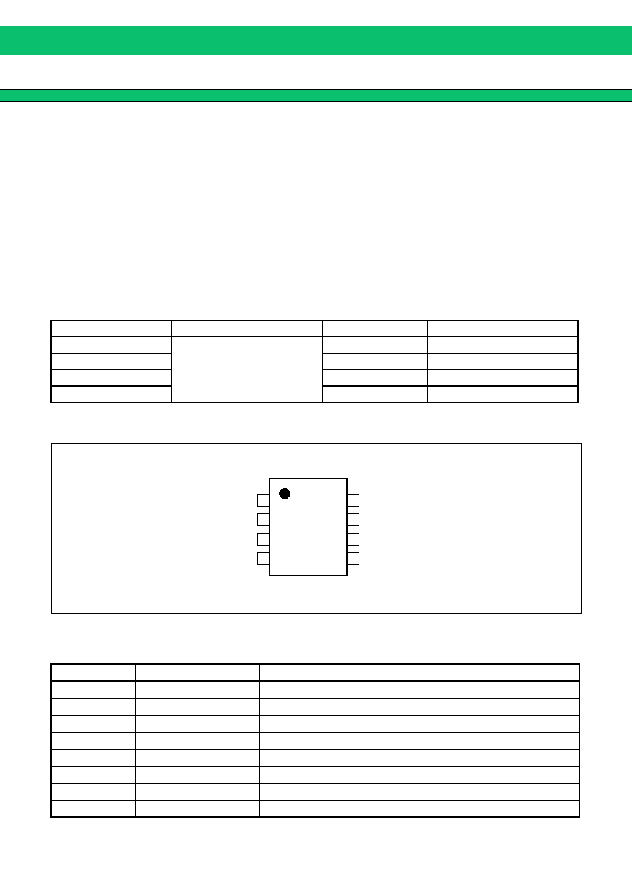
PRODUCT LINEUP
MB88151 has four kinds of multiplication type.
PIN ASSIGNMENT
PIN DESCRIPTION
Product
Input frequency range
Multiplier ratio
Output frequency range
MB88151-100
16.6 MHz to 33.4 MHz
Multiplied by 1
16.6 MHz to 33.4 MHz
MB88151-200
Multiplied by 2
33.3 MHz to 66.7 MHz
MB88151-400
Multiplied by 4
66.6 MHz to 133.4 MHz
MB88151-500
Multiplied by 1/2
8.3 MHz to 16.7 MHz
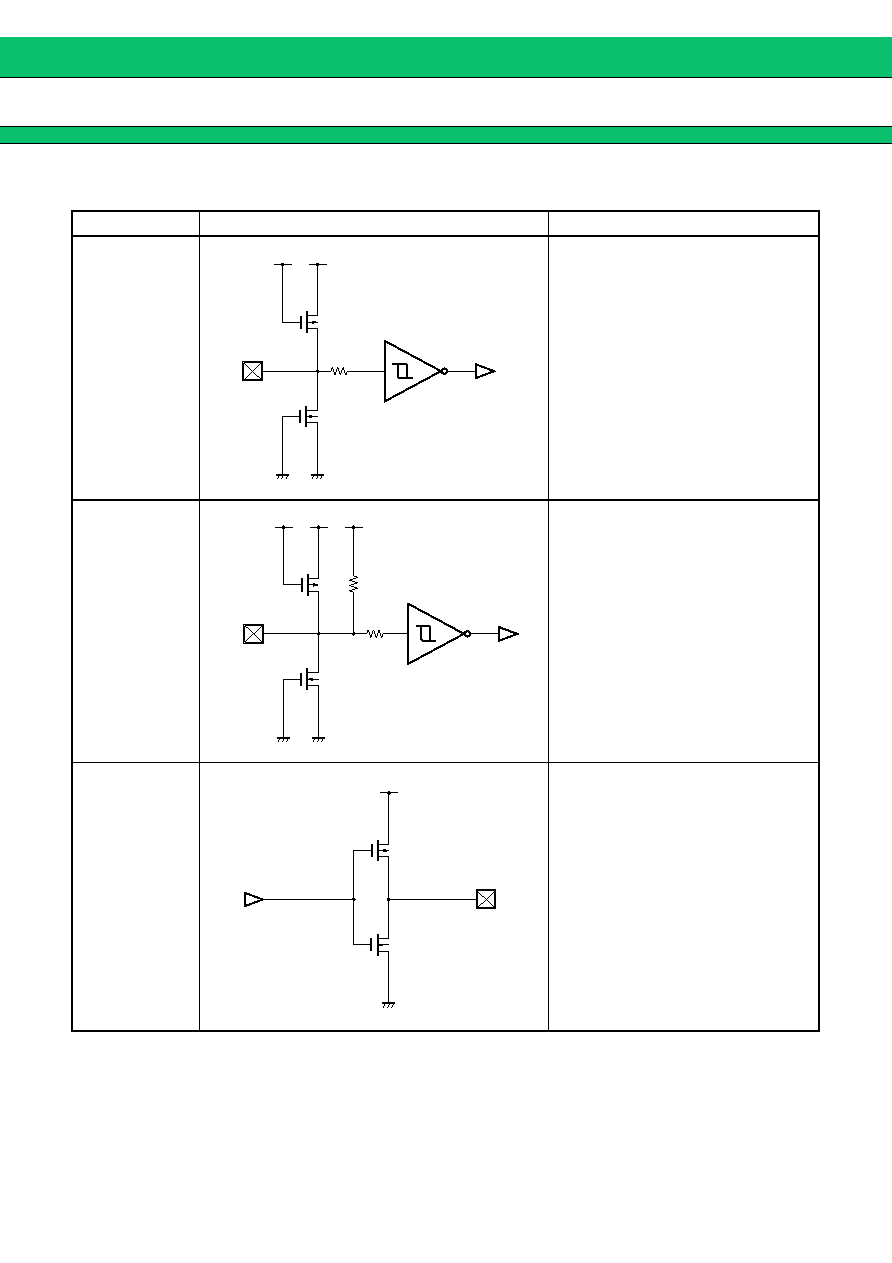
Pin name
I/O
Pin no.
Description
XIN
I
1
Resonator connection pin/clock input pin
V
SS
2
GND pin
SEL0
I
3
Modulation rate setting pin
SEL1
I
4
Modulation rate setting pin
CKOUT
O
5
Modulated clock output pin
ENS
I
6
Modulation enable setting pin (with pull-up resistance)
V
DD
7
Power supply voltage pin
XOUT
O
8
Resonator connection pin
1
2
3
4
8
7
6
5
XIN
V
SS
SEL0
SEL1
XOUT
V
DD
ENS
CKOUT
MB88151
TOP VIEW
FPT-8P-M02

MB88151
4
HANDLING DEVICES
Preventing Latchup
A latchup can occur if, on this device, (a) a voltage higher than V
DD
or a voltage lower than V
SS
is applied to an
input or output pin or (b) a voltage higher than the rating is applied between V
DD
and V
SS
. The latchup, if it occurs,
significantly increases the power supply current and may cause thermal destruction of an element. When you
use this device, be very careful not to exceed the maximum rating.
Handling unused pins
Do not leave an unused input pin open, since it may cause a malfunction. Handle by, using a pull-up or
pull-down resistor.
Unused output pin should be opened.
The attention when the external clock is used
Input the clock to XIN pin, and XOUT pin should be opened when you use the external clock.
Please pay attention so that an overshoot and an undershoot do not occur to an input clock of XIN pin.
Power supply pins
Please design connecting the power supply pin of this device by as low impedance as possible from the current
supply source.
We recommend connecting electrolytic capacitor (about 10
µ
F) and the ceramic capacitor (about 0.01
µ
F) in
parallel between V
SS
and V
DD
near the device, as a bypass capacitor.
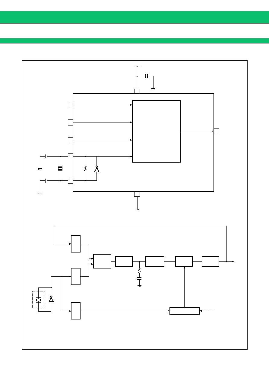
Oscillation circuit
Noise near the XIN and XOUT pins may cause the device to malfunction. Design printed circuit boards so that
electric wiring of XIN or XOUT pin and the resonator do not intersect other wiring.
Design the printed circuit board that surrounds the XIN and XOUT pins with ground.