 | –≠–ª–µ–∫—Ç—Ä–æ–Ω–Ω—ã–π –∫–æ–º–ø–æ–Ω–µ–Ω—Ç: NB90234 | –°–∫–∞—á–∞—Ç—å:  PDF PDF  ZIP ZIP |

DS07-13504-2E
FUJITSU SEMICONDUCTOR
DATA SHEET
16-bit Proprietary Microcontroller
CMOS
F
2
MC-16F MB90230 Series
MB90233/234/P234/W234
s
DESCRIPTION
The MB90230 series is a member of general-purpose, 16-bit microcontrollers designed for those applications which
require high-speed realtimeprocessing, proving to be suitable for various industrial machines, camera and video
devices, OA equipment, and for process control. The CPU used in this series is the F
2
MC*-16F. The instruction
set for the F
2
MC-16F CPU core is designed to be optimized for controller applications while inheriting the AT
architecture of the F
2
MC-16/16H series, allowing a wide range of control tasks to be processed efficiently at high
speed.
The peripheral resources integrated in the MB90230 series include: the UART (clock asynchronous/synchronous
transfer)
◊
1 channel, the extended serial I/O interface
◊
1 channel, the A/D converter (8/10-bit precision)
◊
8
channels, the D/A converter (8-bit precision)
◊
2 channels, the level comparator
◊
1 channel, the external interrupt
input
◊
4 lines, the 8-bit PPG timer (PWM/single-shot function)
◊
1 channel, the 8-bit PWM controller
◊
6 channels,
the 16-bit free run timer
◊
1 channel, the input capture unit
◊
4 channels, the output compare unit
◊
6 channels,
and the serial E
2
PROM interface.
*: F
2
MC stands for FUJITSU Flexible Microcontroller.
s
FEATURES
F
2
MC-16F CPU block
∑ Minimum execution time: 62.5 ns (at machine clock frequency of 16 MHz)
∑ Instruction set optimized for controllers
Various data types supported (bit, byte, word, and long-word)
Extended addressing modes: 23 types
High coding efficiency
Higher-precision operation enhanced by a 32-bit accumulator
Signed multiplication and division instructions
(Continued)
s
PACKAGE
100-pin Plastic LQFP
(FPT-100P-M05)
100-pin Ceramic LQFP
(FPT-100C-C01)

MB90230 Series
2
(Continued)
∑ Enhanced instructions applicable to high-level language (C) and multitasking
System stack pointer
Enhanced pointer-indirect instructions
Barrel shift instructions
∑ Increased execution speed: 8-byte instruction queue
∑ 8-level, 32-factor powerful interrupt service functions
∑ Automatic transfer function independent of the CPU (EI
2
OS)
∑ General-purpose ports: Up to 84 lines
Ports with input pull-up resistor available: 24 lines
Ports with output open-drain available: 9 lines
Peripheral blocks
∑ ROM:48 Kbytes (MB90233)
96 Kbytes (MB90234)
EPROM: 96 Kbytes (MB90W234)
One-time PROM: 96 Kbytes (MB90P234)
∑ RAM: 2 Kbytes (MB90233)
3 Kbytes (MB90234/W234/P234)
∑ PWM control circuit: (simple 8 bits): 6 channels
∑ Serial interface
UART: 1 channel
Extended serial I/O interface
Switchable I/O port: 1 channel
Communication prescaler (Source clock generator for the UART, serial I/O interface, CKOT, and level
comparator): 1 channel
∑ Serial E
2
PROM interface: 1 channel
∑ A/D converter with 8/10-bit resolution: input 8 channels
∑ Level comparator: 1 channel
4-bit D/A converter integrated
∑ D/A converter with 8-bit resolution: 2 channels
8-bit PPG timer: 1 channel
∑ Input/output timer
16-bit free run timer: 1 channel
16-bit output compare unit: 6 channels
16-bit input capture unit: 4 channels
∑ 18-bit timebase timer
∑ Watchdog timer function
∑ Standby modes
Sleep mode
Stop mode
3
MB90230 Series
s
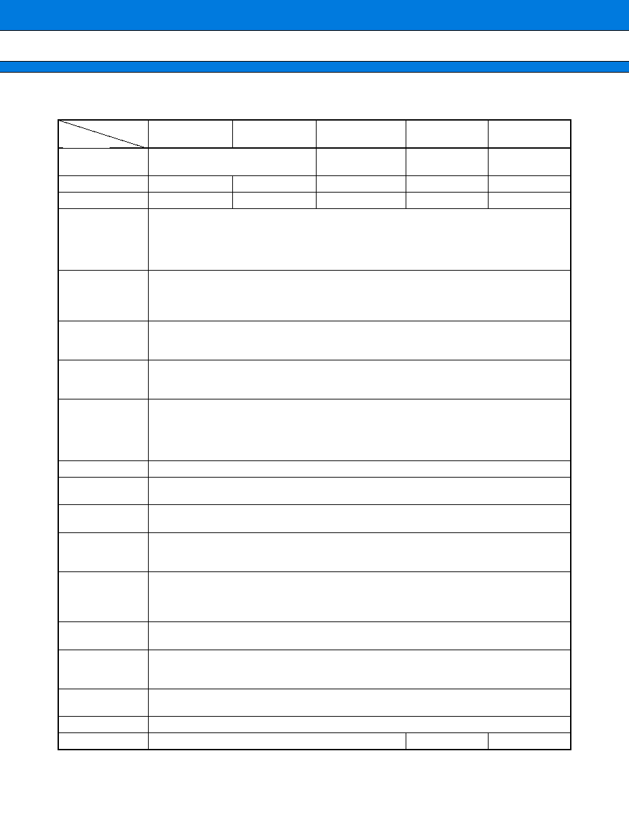
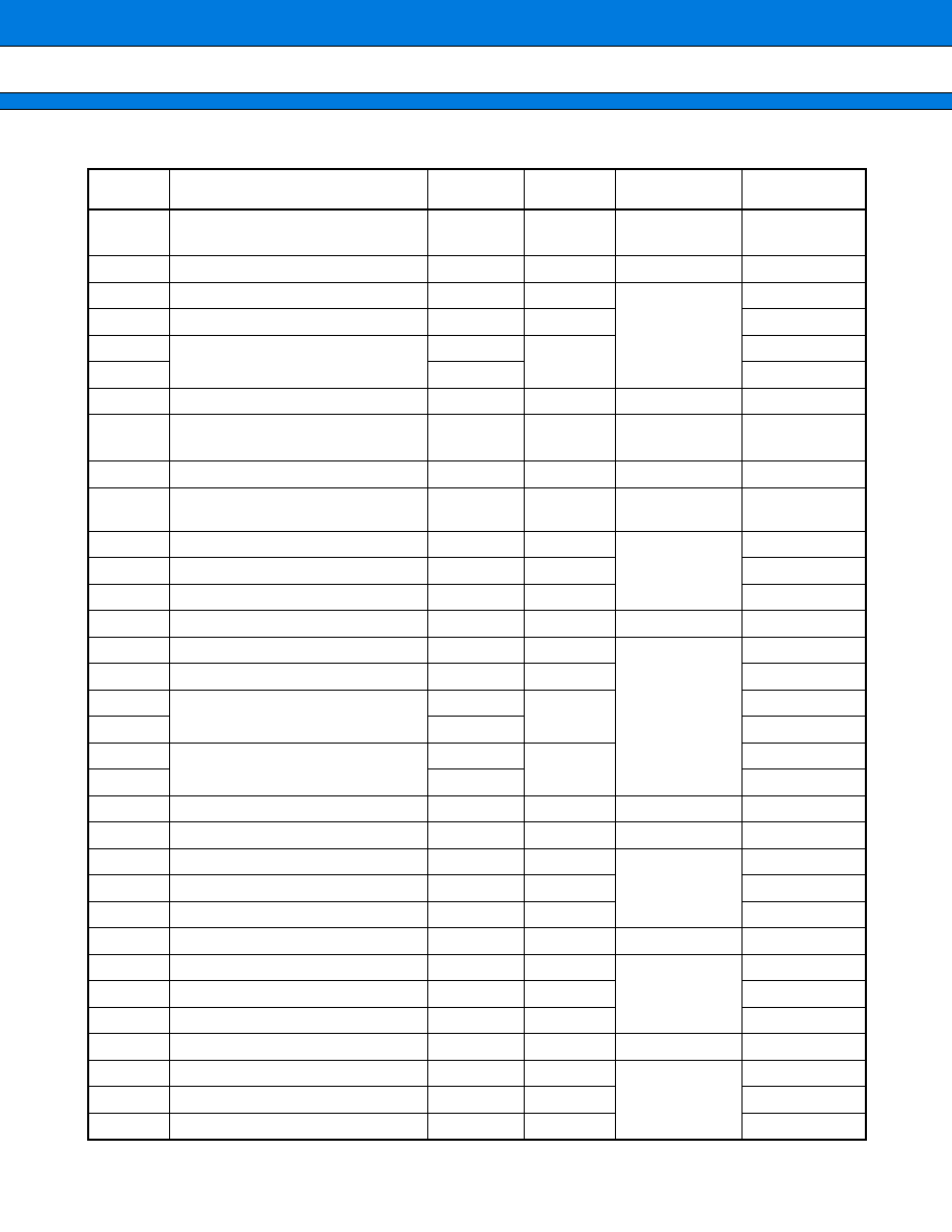
PRODUCT LINEUP
NB90234
MB90P234
MB90W234
MB90V230
Classification
Mask ROM products
One-time PROM
model
EPROM model
Evaluation
model
ROM size
48 Kbytes
96 Kbytes
96 Kbytes
96 Kbytes
--
RAM size
2 Kbytes
3 Kbytes
3 Kbytes
3 Kbytes
4 Kbytes
CPU functions
Number of instructions: 420
Instruction bit length: 8 or 16 bits
Instruction length: 1 to 7 bytes
Data bit length: 1, 4, 8, 16, or 32 bits
Minimum execution time: 62.5 ns at 16 MHz (internal)
Ports
Up to 84 lines
I/O ports (CMOS): 51
I/O ports (CMOS) with pull-up resistor available: 24
I/O ports (open-drain): 9
UART
Number of channels: 1 (switchable I/O)
Clock synchronous communication (2404 to 38460 bps, full-duplex double buffering)
Clock asynchronous communication (500K to 5M bps, full-duplex double buffering)
Serial interface
Number of channels: 1
Internal or external clock mode
Clock synchronous transfer (62.5 kHz to 1 MHz, "LSB first" or "MSB first" transfer)
A/D converter
Resolution: 10 or 8 bits, Number of input lines: 4
Single conversion mode (conversion for a specified input channel)
Scan conversion mode (continuous conversion for specified consecutive channels)
Continuous conversion mode (repeated conversion for a specified channel)
Stop conversion mode (periodical conversion)
D/A converter
Resolution: 8 bits, Number of output pins: 2
Level
comparator
Comparison to internal D/A converter (4-bit resolution)
PWM
Number of channels: 6
8-bit PWM control circuit (operation of 1
◊
, 2
◊
, 16
◊
, 32
◊
)
PPG timer
Number of channels: 1 channel with 8-bit resolution
PWM function: Continuous output of pulse synchronous to trigger
Single-shot function: Output of single pulse by trigger
Serial E
2
PROM
interface
Number of channels: 1
Instruction code (NS type)
Variable address length: 8 to 11 bits (with address increment function)
Variable data length: 8 or 16 bits
Timer
Number of channels: 6
16-bit reload timer operation (operation clock cycle of 0.25
µ
s to 1.05 s)
Free run timer
Number of channels: 1
16-bit input capture unit: 4 channels
16-bit output compare unit: 6 channels
External interrupt
input
Number of input pins: 4
Standby mode
Stop mode and sleep mode
Package
FPT-100P-M05
FPT-100C-C01
PGA256-A02
MB90233
Parameter
Part number

MB90230 Series
4
s
PIN ASSIGNMENT
75
74
73
72
71
70
69
68
67
66
65
64
63
62
61
60
59
58
57
56
55
54
53
52
51
RST
P54/WRH
P53/HRQ
P52/HAK
P51/RDY
P50/CLK
PA5/SCK2
PA4/SOT2
PA3/SIN2
PA2/SCK1
PA1/SOT1
PA0/SIN1
P96/SCK0
P95/SOT0
P94/SIN0
P93/IN3/CKOT
P92/IN2
P91/IN1
P90/IN0
P87/OUT5
P86/OUT4
P85/OUT3
P84/OUT2
P83/OUT1/INT3
P82/OUT0/INT2
1
2
3
4
5
6
7
8
9
10
11
12
13
14
15
16
17
18
19
20
21
22
23
24
25
P22/A02
P23/A03
P24/A04
P25/A05
P26/A06
P27/A07
P30/A08
P31/A09
V
SS
P32/A10
P33/A11
P34/A12
P35/A13
P36/A14
P37/A15
PWM0/P40/A16
PWM1/P41/A17
PWM2/P42/A18
PWM3/P43/A19
PWM4/P44/A20
V
CC
PWM5/P45/A21
TRG/P46/A22
PPG/P47/A23
ATG/P70
P71/EDI
P72/EDO
P73/ESK
P74/ECS
P75/DA0
P76/DA1
AV
CC
AVRH
AVRL
AV
SS
P60/AN0
P61/AN1
P62/AN2
P63/AN3
V
SS
P64/AN4
P65/AN5
P66/AN6
P67/AN7/CMP
P80/INT0
P81/INT1
MD0
MD1
MD2
HST
P21/A01
P20/A00
P17/D15
P16/D14
P15/D13
P14/D12
P13/D11
P12/D10
P11/D09
P10/D08
P07/D07
P06/D06
P05/D05
P04/D04
P03/D03
P02/D02
P01/D01
P00/D00
V
CC
X1
X0
V
SS
P57
P56/RD
P55/WRL
(TOP VIEW)
26
27
28
29
30
31
32
33
34
35
36
37
38
39
40
41
42
43
44
45
46
47
48
49
50
100
99
98
97
96
95
94
93
92
91
90
89
88
87
86
85
84
83
82
81
80
79
78
77
76
(FPT-100P-M05)
(FPT-100C-C01)
5
MB90230 Series
s
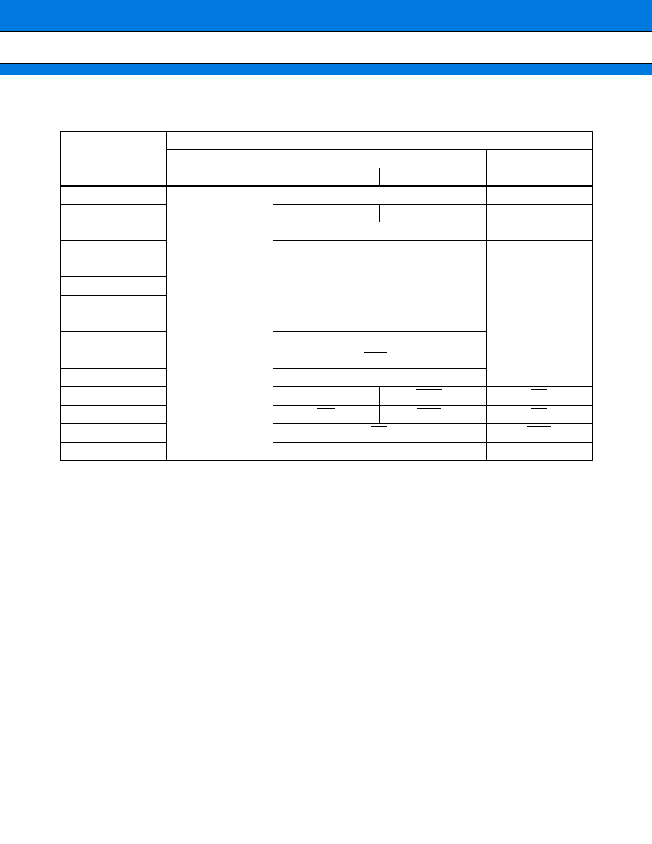
PIN DESCRIPTION
(Continued)
Pin no.
Pin name
Circuit
type
Function
80
X0
A
Oscillator pins
81
X1
82
V
CC
--
Power supply pin
83 to 90
P00 to P07
G
General-purpose I/O port
An input pull-up resistor can be added to the port by setting the
pull-up resistor setting register.
These pins serve as D00 to D07 pins in bus modes other than the
single-chip mode.
D00 to D07
I/O pins for the lower eight bits of the external data bus.
These pins are enabled in an external-bus enabled mode.
91 to 98
P10 to P17
G
General-purpose I/O port
An input pull-up resistor can be added to the port by setting the pull-up
resistor setting register.
These pins are enabled in the single-chip mode with the external-bus
enabled and the 8-bit data bus specified.
D08 to D15
I/O pins for the upper eight bits of the external data bus
These pins are enabled in an external-bus enabled mode with the 16-
bit data bus specified.
99, 100
1 to 6
P20 to P27
G
General-purpose I/O port
An input pull-up resistor can be added to the port by setting the
pull-up resistor setting register.
These pins are enabled in the single-chip mode.
A00 to A07
I/O pins for the lower eight bits of the external data bus
These pins are enabled in an external-bus enabled mode.
7, 8
P30, P31
E
General-purpose I/O port
This port is enabled in the single-chip mode or when the middle
address control register setting is "port."
A08, A09
I/O pins for the middle eight bits of the external data bus
These pins are enabled in an external-bus enabled mode when the
middle address control register setting is "address."
9
V
SS
--
Power supply pin
10 to 15
P32 to P37
E
General-purpose I/O port
This port is enabled in the single-chip mode or when the middle
address control register setting is "port."
A10 to A15
I/O pins for the middle eight bits of the external data bus
These pins are enabled in an external-bus enabled mode when the
middle address control register setting is "address."
MB90230 Series
6
(Continued)
Pin no.
Pin name
Circuit
type
Function
16
P40
E
General-purpose I/O port
This port is enabled in the single-chip mode or when the upper
address control register setting is "port."
A16
Output pin for external address A16
This pin is enabled in the external-bus enabled mode with the upper
address control register set to "address."
PWM0
This pin serves as the output pin for 8-bit PWM0
The pin is enabled for output by the control status register.
17
P41
E
General-purpose I/O port
This port is enabled in the single-chip mode or when the upper
address control register setting is "port."
A17
Output pin for external address A17
This pin is enabled in the external-bus enabled mode with the upper
address control register set to "address."
PWM1
This pin serves as the output pin for 8-bit PWM1.
The pin is enabled for output by the control status register.
18
P42
E
General-purpose I/O port
This port is enabled in the single-chip mode or when the upper
address control register setting is "port."
A18
Output pin for external address A18
This pin is enabled in the external-bus enabled mode with the upper
address control register set to "address."
PWM2
This pin serves as the output pin for 8-bit PWM2.
This pin is enabled for output by the control status register.
19
P43
E
General-purpose I/O port
This port is enabled in the single-chip mode or when the upper
address control register setting is "port."
A19
Output pin for external address A19
This pin is enabled in the external-bus enabled mode with the upper
address control register set to "address."
PWM3
This pin serves as the output pin for 8-bit PWM3.
This pin is enabled for output by the control status register.
20
P44
E
General-purpose I/O port
This port is enabled in the single-chip mode or when the upper
address control register setting is "port."
A20
Output pin for external address A20
This pin is enabled in the external-bus enabled mode with the upper
address control register set to "address."
PWM4
This pin serves as the output pin for 8-bit PWM4.
The pin is enabled for output by the control status register.
21
V
CC
--
Power supply pin
7
MB90230 Series
(Continued)
Pin no.
Pin name
Circuit
type
Function
22
P45
E
General-purpose I/O port
This port is enabled in the single-chip mode or when the upper
address control register setting is "port."
A21
Output pin for external address A21
This pin is enabled in the external-bus enabled mode with the upper
address control register set to "address."
PWM5
This pin serves as the output pin for 8-bit PWM5.
The pin is enabled for output by the control status register.
23
P46
L*
1
General-purpose I/O port
This port is enabled in the single-chip mode or when the upper
address control register setting is "port."
A22
Output pin for external address A22
This pin is enabled in the external-bus enabled mode with the upper
address control register set to "address."
TRG
This pin serves as the external trigger pin for the 8-bit PPG timer
The pin is enabled for triggering by the control status register.
24
P47
E
General-purpose I/O port
This port is enabled in the single-chip mode or when the upper
address control register setting is "port."
A23
Output pin for external address A23
This pin is enabled in the external-bus enabled mode with the upper
address control register set to "address."
PPG
This pin serves as the output pin for the 8-bit PPG timer.
The pin is enabled for output by the control status register.
25
P70
L*
1
General-purpose I/O port
ATG
External trigger input pin for the A/D converter
This pin functions when enabled by the control status register.
26
P71
F
General-purpose I/O port
EDI
Data input pin for the serial EEPROM interface
This pin functions when enabled by the control status register.
27
P72
E
General-purpose I/O port
EDO
Data output pin for the serial EEPROM interface
This pin functions when enabled by the control status register.
28
P73
E
General-purpose I/O port
ESK
Clock output pin for the serial EEPROM interface
This pin functions when enabled by the control status register.
29
P74
E
General-purpose I/O port
ECS
Chip select signal output pin for the serial EEPROM interface
This pin functions when enabled by the control status register.
MB90230 Series
8
(Continued)
Pin no.
Pin name
Circuit
type
Function
30, 31
P75, P76
K
General-purpose I/O port
DA0
DA1
This pin serves as the D/A converter output pin.
The pin functions when enabled by the control status register.
32
AV
CC
--
A/D converter power supply pin
33
AV
RH
--
"H" reference power supply pin for the A/D converter
34
AV
RL
--
"L" reference power supply pin for the A/D converter
35
AV
SS
--
A/D converter power pin (GND)
36 to 39
P60 to P63
J
General-purpose I/O port
This port is enabled when the analog input enable register setting is
"port."
AN0 to AN3
A/D converter analog input pins
These pins are enabled when the analog input enable register setting
is "analog input."
40
V
SS
--
Power pin (GND)
41 to 43
P64 to P66
J
General-purpose I/O port
This port is enabled when the analog input enable register setting is
"port."
AN4 to AN6
A/D converter analog input pins
These pins are enabled when the analog input enable register setting
is "analog input."
44
P67
J
General-purpose I/O port
This port is enabled when the analog input enable register setting is
"port."
AN7
A/D converter analog input pin
This pin is enabled when the analog input enable register setting is
"analog input."
CMP
Comparator input pin
45
P80
L*
2
General-purpose I/O port
This port is always enabled.
INT0
External interrupt request input 0
Since this pin serves for interrupt request as required when external
interrupt is enabled, other outputs must be off unless used
intentionally.
46
P81
L*
2
General-purpose I/O port
This port is always enabled.
INT1
External interrupt request input 1
Since this pin serves for interrupt request as required when external
interrupt is enabled, other outputs must be off unless used
intentionally.
47
MD0
C
Mode pin
This pin must be fixed to V
CC
or V
SS
.
48
MD1
C
Mode pin
This pin must be fixed to V
CC
or V
SS
.
9
MB90230 Series
(Continued)
Pin no.
Pin name
Circuit
type
Function
49
MD2
C
Mode pin
This pin must be fixed to V
SS
.
50
HST
D
Hardware standby input pin
51, 52
P82, P83
L*
2
General-purpose I/O port
OUT0,
OUT1
Output compare output pins
These pins function when enabled by the control status register.
INT2,
INT3
External interrupt request inputs 2 and 3.
Since these pins serve for interrupt request as required when external
interrupt is enabled, other outputs must be off unless used
intentionally.
53 to 56
P84 to P87
E
General-purpose I/O port
This pin is always enabled.
OUT2 to OUT5
Output compare output pins
These pins function when enabled by the control status register.
57 to 59
P90 to P92
L*
1
General-purpose I/O port
This port is always enabled.
IN0 to IN2
Input capture edge input pins
These pins function when enabled by the control status register.
60
P93
L*
1
General-purpose I/O port
This port is always enabled.
IN3
Input capture edge input pin
This pin functions when enabled by the control status register.
CKOT
Prescaler output pin
This pin functions when enabled by the control status register.
61
P94
I
General-purpose I/O port
This port is always enabled.
The port serves as an open-drain output depending on the open-drain
setting register.
SIN0
Serial data input pin for the UART
This pin functions when enabled by the control status register.
62
P95
H
General-purpose I/O port
This port is always enabled.
The port serves as an open-drain output depending on the open-drain
setting register.
SOT0
Serial data output pin for the UART
This pin functions when enabled by the control status register.
63
P96
I
General-purpose I/O port
This port is always enabled.
The port serves as an open-drain output depending on the open-drain
setting register.
SCK0
UART clock output pin
This pin functions when enabled by the control status register.

MB90230 Series
10
(Continued)
Pin no.
Pin name
Circuit
type
Function
64
PA0
I
General-purpose I/O port
This port is always enabled.
The port serves as an open-drain output depending on the open-drain
setting register.
SIN1
Serial data input pin for the extended serial I/O interface
This pin functions when enabled by the control status register and by
the serial port switching register.
65
PA1
H
General-purpose I/O port
This port is always enabled.
The port serves as an open-drain output depending on the open-drain
setting register.
SOT1
Serial data output pin for the extended serial I/O interface
This pin functions when enabled by the control status register and by
the serial port switching register.
66
PA2
I
General-purpose I/O port
This port is always enabled.
The port serves as an open-drain output depending on the open-drain
setting register.
SCK1
Clock output pin for the extended serial I/O interface
This pin functions when enabled by the control status register and by
the serial port switching register.
67
PA3
I
General-purpose I/O port
This port is always enabled.
The port serves as an open-drain output depending on the open-drain
setting register.
SIN2
Serial data input pin for the extended serial I/O interface
This pin functions when enabled by the control status register and by
the serial port switching register.
68
PA4
H
General-purpose I/O port
This port is always enabled.
The port serves as an open-drain output depending on the open-drain
setting register.
SOT2
Serial data output pin for the extended serial I/O interface
This pin functions when enabled by the control status register and by
the serial port switching register.
69
PA5
I
General-purpose I/O port
This port is always enabled.
The port serves as an open-drain output depending on the open-drain
setting register.
SCK2
Clock output pin for the extended serial I/O interface
This pin functions when enabled by the control status register and by
the serial port switching register.
The pin is a general-purpose I/O port.

11
MB90230 Series
(Continued)
*1: Enabled in any standby mode
*2: Enabled only in the hardware standby mode
Pin no.
Pin name
Circuit
type
Function
70
P50
H
This pin is enabled in the single-chip mode and when the CLK output
is disabled.
CLK
CLK output pin
This pin is enabled in an external-bus enabled mode with the CLK
output enabled.
71
P51
F
General-purpose I/O port
This port is enabled in the single-chip mode.
RDY
Ready signal input pin
This pin is enabled in an external-bus enabled mode.
72
P52
E
General-purpose I/O port
This port is enabled in the single-chip mode or when the hold function
is disabled.
HAK
Hold acknowledge signal output pin
This pin is enabled in the single-chip mode or when the hold function
is enabled.
73
P53
E
General-purpose I/O port
This port is enabled in the single-chip mode or when the hold function
is disabled.
HRQ
Hold acknowledge signal output pin
This pin is enabled in the single-chip mode or when the hold function
is enabled.
74
P54
E
General-purpose I/O port
This port is enabled in the single-chip mode, in external-bus 8-bit
mode, or when the WR pin output is disabled.
WRH
Write strobe output pin for the upper eight bits of the data bus
This pin is enabled in an external-bus enabled mode and in external
bus 16-bit mode with the WR pin output enabled.
75
RST
B
Reset signal input pin
76
P55
E
This port is enabled in the single-chip mode, in external-bus 8-bit
mode, or when the WR pin output is disabled
WRL
Write strobe output pin for the lower eight bits of the data bus
This pin is enabled in an external-bus enabled mode and in external
bus 16-bit mode with the WR pin output enabled.
The pin is a general-purpose I/O port.
77
P56
E
This pin is enabled in the single-chip mode.
RD
Read strobe output pin for the data bus
This pin is enabled in an external-bus enabled mode.
78
P57
E
General-purpose I/O port
79
V
SS
--
Power pin (GND)

MB90230 Series
12
s
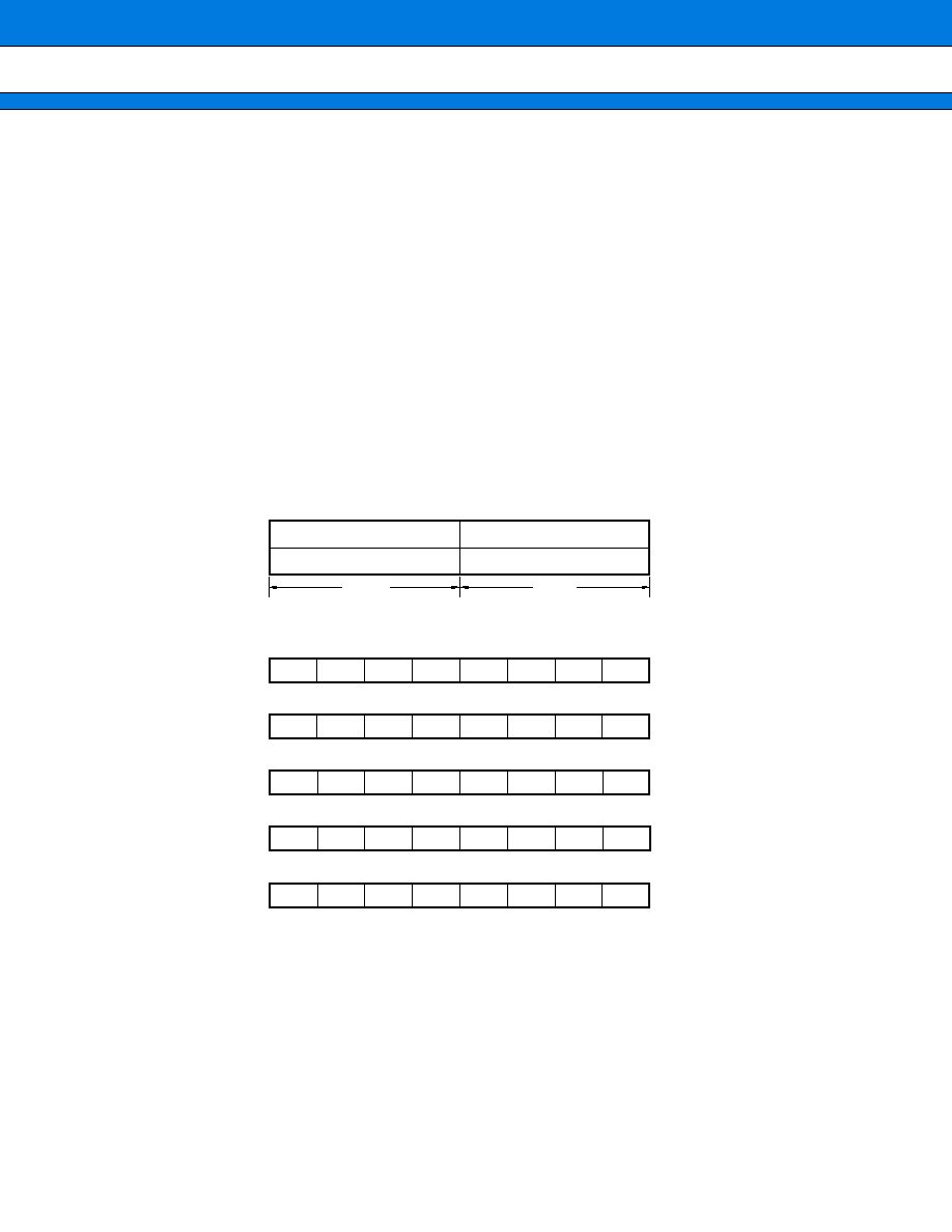
I/O CIRCUIT TYPE
(Continued)
Type
Circuit
Remarks
A
∑ Oscillation feedback resistor:
Approx. 1 M
B
∑ Hysteresis input with pull-up
resistor
C
∑ CMOS input port
D
∑ Hysteresis input port
E
∑ CMOS level output
X1
X0
Standby control
Standby control
CMOS

13
MB90230 Series
(Continued)
Type
Circuit
Remarks
F
∑ CMOS level output
∑ Hysteresis input
G
∑ Input pull-up resistor control
provided
∑ CMOS level input/output
H
∑ CMOS level input/output
∑ Open-drain control provided
Standby control
Standby control
CMOS
Pull-up control
CMOS
Open-drain control signal
Standby control

MB90230 Series
14
(Continued)
Type
Circuit
Remarks
I
∑ CMOS level output
∑ Hysteresis input
∑ Open-drain control provided
J
∑ CMOS level input/output
∑ Analog input
K
∑ CMOS level input/output
∑ Analog output
∑ Also serving for D/A output
L
∑ CMOS level output
∑ Hysteresis input
∑ Open-drain control provided
CMOS
Open-drain control signal
Standby control
CMOS
Analog input
Standby control
CMOS
DA output
Standby control
Standby control
Open-drain control signal
15
MB90230 Series
s
HANDLING DEVICES
1. Preventing Latchup
Latchup may occur on CMOS ICs if voltage higher than V
CC
or lower than V
SS
is applied to input and output pins
other than medium- to high-voltage pins or if higher than the voltage wihich shows on "1. Absolute Maximum
Ratings" in section "
s
Electrical Characteristics" is applied between V
CC
and V
SS
.
When latchup occurs, power supply current increases rapidly and might thermally damage elements. When
using, take great care not to exceed the absolute maximum ratings.
Also, take care to prevent the analog power supply (AV
CC
and AVR) and analog input from exceeding the digital
power supply (V
CC
) when the analog system power supply is turned on and off.
2. Treatment of Unused Pins
Leaving unused input pins open could cause malfunctions. They should be connected to a pull-up or pull-down
resistor.
3. External Reset Input
To reset the internal circuit by the Low-level input to the RST pin, the Low-level input to the RST pin must be
maintained for at least five machine cycles. Pay attention to it if the chip uses external clock input.
4. V
CC
and V
SS
Pins
Apply equal potential to the V
CC
and V
SS
pins.
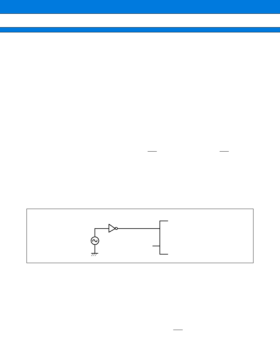
5. Notes on Using an External Clock
When using an external clock, drive the X0 pin as illustrated below:
6. Power-on Sequence for A/D Converter Power Supplies and Analog Inputs
Be sure to turn on the digital power supply (V
CC
) before applying voltage to the A/D converter power supplies
(AV
CC
, AVRH, and AVRL) and analog inputs (AN0 to AN15).
When turning power supplies off, turn off the A/D converter power supplies (AV
CC
, AVRH, and AVRL) and analog
inputs (AN0 to AN15) first, then the digital power supply (AV
CC
).
When turning AVRH on or off, be careful not to let it exceed AV
CC
.
7. Pin set when turning on power supplies
When turning on power supplies, set the hardware standby input pin (HST) to "H".
Use of External Clock
X0
X1
MB90234

MB90230 Series
16
8. Program Mode
When shipped from Fujitsu, and after each erasure, all bits (96K
◊
8 bits) in the MB90W234 and MB90P234 are
in the "1" state. Data is introduced by selectively programming "0's" into the desired bit locations. Bits cannot
be set to 1 electrically.
9. Erasure Procedure
Data written in the MB90W234 is erased (from 0 to 1) by exposing the chip to ultraviolet rays with a wavelength
of 2,537≈ through the translucent cover.
Recommended irradiation dosage for exposure is 10 Wsec/cm
2
. This amount is reached in 15 to 20 minutes
with a commercial ultraviolet lamp positioned 2 to 3 cm above the package (when the package surface
illuminance is 1200
µ
W/cm
2
).
If the ultraviolet lamp has a filter, remove the filter before exposure. Attaching a mirrored plate to the lamp
increases the illuminance by a factor of 1.4 to 1.8, thus shortening the required erasure time. If the translucent
part of the package is stained with oil or adhesive, transmission of ultraviolet rays is degraded, resulting in a
longer erasure time. In that case, clean the translucent part using alcohol (or other solvent not affecting the
package).
The above recommended dosage is a value which takes the guard band into consideration and is a multiple of
the time in which all bits can be evaluated to have been erased. Observe the recommended dosage for erasure;
the purpose of the guard band is to ensure erasure in all temperature and supply voltage ranges. In addition,
check the lifespan of the lamp and control the illuminance appropriately.
Data in the MB90W234 is erased by exposure to light with a wavelength of 4000≈ or less.
Data in the device is also erased even by exposure to fluorescent lamp light or sunlight although the exposure
results in a much lower erasure rate than exposure to 2537≈ ultraviolet rays. Note that exposure to such lights
for an extended period will therefore affect system reliability. If the chip is used where it is exposed to any light
with a wavelength of 4000≈ or less, cover the translucent part, for example, with a protective seal to prevent
the chip from being exposed to the light.
Exposure to light with a wavelength of 4,000 to 5,000≈ or more will not erase data in the device. If the light
applied to the chip has a very high illuminance, however, the device may cause malfunction in the circuit for
reasons of general semiconductor characteristics. Although the circuit will recover normal operation when
exposure is stopped, the device requires proper countermeasures for use in a place exposed continuously to
such light even though the wavelength is 4,000≈ or more.

17
MB90230 Series
10. Recommended Screening Conditions
High-temperature aging is recommended for screening before packaging.
11. Write Yield
OTPROM products cannot be write-tested for all bits due to their nature. Therefore the write yield cannot always
be guaranteed to be 100%.
Program, verify
Aging
+150∞C, 48 Hrs.
Data verification
Assembly

MB90230 Series
18
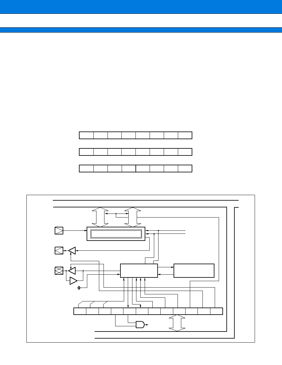
s
BLOCK DIAGRAM
RAM
Interrupt controller
F
2
MC-16 bus
8
8
8
8
8
8
8
7
8
P00
to
P07
P10
to
P17
P20
to
P27
P30
to
P37
P40
to
P47
P50
to
P57
P60
to
P67
P70
to
P76
P80
to
P87
I/O ports (84 lines)
CPU
F
2
MC-16F
ROM
8-bit PPG timer
I/O timer
IN0, 1
IN2, 3
Level comparator
7
P90
to
P96
CMP
6
PA0
to
PA5
4
X0, X1
RST
HST
TRG
PPG
External interrupt
UART
SIN0
SOT0
SCK0
CKOT
Extended serial
I/O interface
SIN1, 2
SOT1, 2
SCK1, 2
10-bit A/D converter
AVcc
AVRH, AVRL
AVss
ATG
AN0 to AN7
D/A converter
16-bit input capture
◊
4
16-bit output compare
◊
6
16-bit free run timer
DA0
DA1
P00 to P27 (24 lines): Provided with input pull-up resistor setting registers
P94 to P96, PA0 to PA5 (9 lines): Provided with open-drain setting registers
INT0
to
INT3
Communication prescaler
4
8-bit PWM
PWM0
to
PWM5
6 ch
OUT0, 1
OUT2, 3
OUT4, 5
Serial E
2
PROM interface
2
ECS, ESK
EDO
EDI
Clock controller
19
MB90230 Series
s
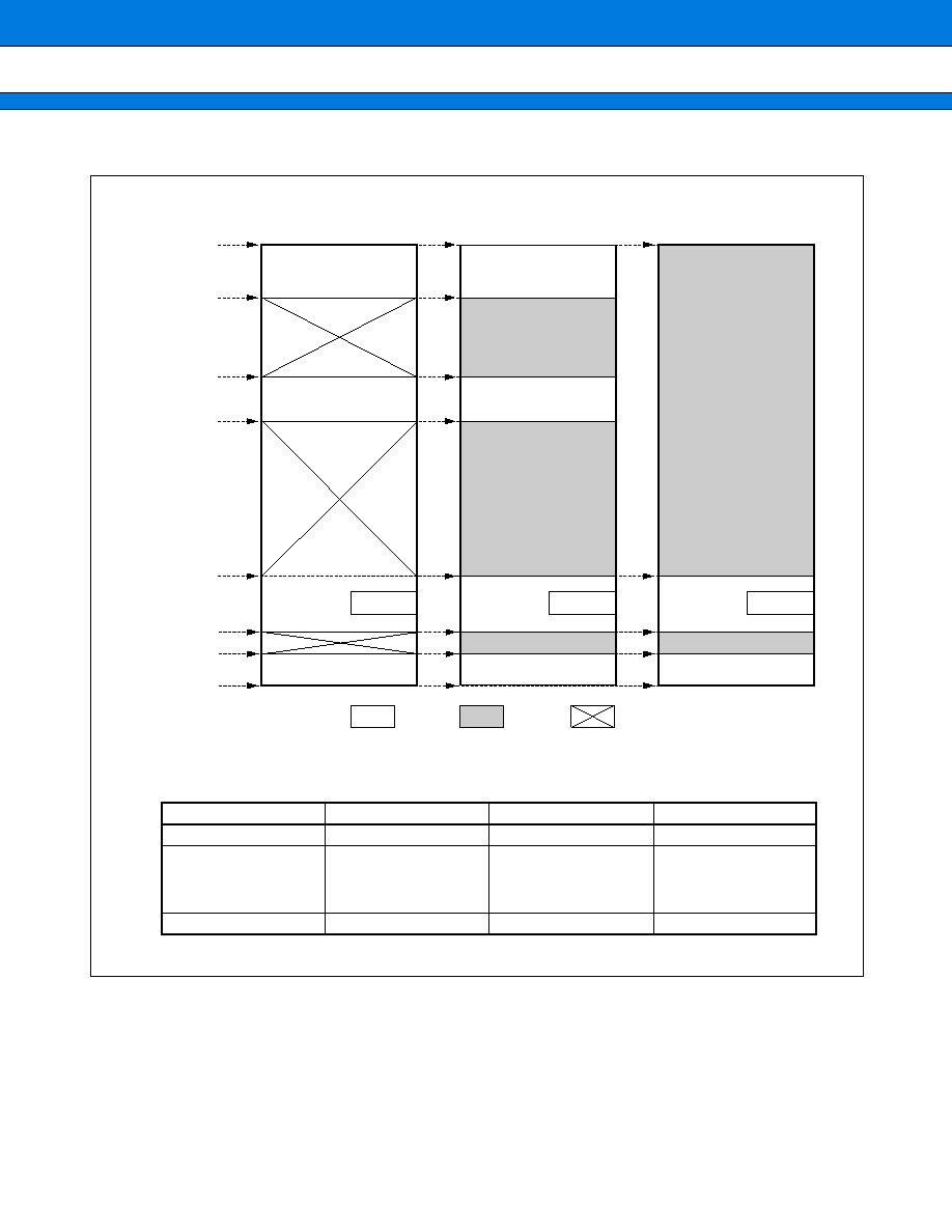
MEMORY MAP
The MB90230 series can access the 00 bank to read ROM data written to the upper 48-KB locations in the FF
bank. An advantage of reading written to data addresses FFFFFF
H
-FF4000
H
from addresses 00FFFF
H
-004000
H
is
that you can use the small model of a C compiler.
Note, however, that the products with more than 48KB ROM space (MB90V230, MB90P/W234, MB90234) cannot
read data in addresses other than FFFFFF
H
to FF4000
H
from the 00 bank.
FFFFFF
H
Address1#
00FFFF
H
Address#2
Address#3
000100
H
0000C0
H
000000
H
Single-chip mode
Internal ROM and
external bus
External ROM and
external bus
ROM area
ROM area
ROM area
(FF bank image)
ROM area
(FF bank image)
RAM
Registers
RAM
Registers
RAM
Registers
Peripherals
Peripherals
Peripherals
Internal
External
Inhibited area
000000
H
to 000005
H
and 000010
H
to 000015
H
are allocated for external use
when the external bus is enabled.
Note:
Address#3
Address#2
Address#1
Product type
MB90233
MB90V230
MB90234
MB90P234
MB90W234
FF4000
H
(FE0000
H
)
FE8000
H
FE8000
H
004000
H
(004000
H
)
004000
H
004000
H
000900
H
(001100
H
)
000D00
H
000D00
H

MB90230 Series
20
s
I/O MAP
(Continued)
Address
Register
Register
name
Access
Resouce
name
Initial value
00
H
Port 0 data register
PDR0
R/W
Port 0
X X X X X X X X
01
H
Port 1 data register
PDR1
R/W
Port 1
X X X X X X X X
02
H
Port 2 data register
PDR2
R/W
Port 2
X X X X X X X X
03
H
Port 3 data register
PDR3
R/W
Port 3
X X X X X X X X
04
H
Port 4 data register
PDR4
R/W
Port 4
X X X X X X X X
05
H
Port 5 data register
PDR5
R/W
Port 5
X X X X X X X X
06
H
Port 6 data register
PDR6
R/W
Port 6
X X X X X X X X
07
H
Port 7 data register
PDR7
R/W
Port 7
≠ X X X X X X X
08
H
Port 8 data register
PDR8
R/W
Port 8
X X X X X X X X
09
H
Port 9 data register
PDR9
R/W
Port 9
≠ X X X X X X X
0A
H
Port A data register
PDRA
R/W
Port A
≠ ≠ X X X X X X
10
H
Port 0 direction register
DDR0
R/W
Port 0
0 0 0 0 0 0 0 0
11
H
Port 1 direction register
DDR1
R/W
Port 1
0 0 0 0 0 0 0 0
12
H
Port 2 direction register
DDR2
R/W
Port 2
0 0 0 0 0 0 0 0
13
H
Port 3 direction register
DDR3
R/W
Port 3
0 0 0 0 0 0 0 0
14
H
Port 4 direction register
DDR4
R/W
Port 4
0 0 0 0 0 0 0 0
15
H
Port 5 direction register
DDR5
R/W
Port 5
0 0 0 0 0 0 0 0
16
H
Port 6 direction register
DDR6
R/W
Port 6
0 0 0 0 0 0 0 0
17
H
Port 7 direction register
DDR7
R/W
Port 7
≠ 0 0 0 0 0 0 0
18
H
Port 8 direction register
DDR8
R/W
Port 8
0 0 0 0 0 0 0 0
19
H
Port 9 direction register
DDR9
R/W
Port 9
≠ 0 0 0 0 0 0 0
1A
H
Port A direction register
DDRA
R/W
Port A
≠ ≠ 0 0 0 0 0 0
1B
H
Port 0 resistor register
RDR0
R/W
Port 0
0 0 0 0 0 0 0 0
1C
H
Port 1 resistor register
RDR1
R/W
Port 1
0 0 0 0 0 0 0 0
1D
H
Port 2 resistor register
RDR2
R/W
Port 2
0 0 0 0 0 0 0 0
1E
H
Port 9 pin register
ODR9
R/W
Port 9
≠ 0 0 0 ≠ ≠ ≠ ≠
1F
H
Port A pin register
ODRA
R/W
Port A
≠ ≠ 0 0 0 0 0 0
20
H
Mode control register
UMC
R/W
UART
0 0 0 0 0 1 0 0
21
H
Status register
USR
R/W
0 0 0 1 0 0 0 0
22
H
Serial input register
/Serial output register
UIDR
/UODR
R/W
X X X X X X X X
23
H
Rate and data register
URD
R/W
0 0 0 0 ≠ ≠ 0 0
24
H
Serial mode control status register
SMCS
R/W
Extended serial
I/O interface
≠ ≠ ≠ 0 0 0 0 0
25
H
0 0 0 0 0 0 1 0
21
MB90230 Series
(Continued)
Address
Register
Register
name
Access
Resouce
name
Initial value
26
H
Serial data register
SDR
R/W
Extended serial
I/O interface
X X X X X X X X
27
H
Reserved area
--
--
--
--
28
H
Cycle setting register
PCSR
W
8-bit
PPG timer
X X X X X X X X
29
H
Duty factor setting register
PDUT
W
X X X X X X X X
2A
H
Control status register
PCNTL
R/W
0 0 0 0 0 0 0 0
2B
H
PCNTH
0 0 0 0 0 0 0 ≠
2C
H
Reserved area
--
--
--
--
2D
H
Communication prescaler
CDCR
R/W
UART, CKOT,
I/O, serial IF
0 ≠ ≠ ≠ 1 1 1 1
2E
H
Clock control register
CLKR
R/W
CKOT output
≠ ≠ ≠ ≠ ≠ 0 0 0
2F
H
Level comparator
LVLC
R/W
Level
comparator
X X X X 0 0 0 0
30
H
Interrupt/DTP enable register
ENIR
R/W
DTP/external
interrupt
≠ ≠ ≠ ≠ 0 0 0 0
31
H
Interrupt/DTP factor register
EIRR
R/W
≠ ≠ ≠ ≠ 0 0 0 0
32
H
Request level setting register
ELVR
R/W
0 0 0 0 0 0 0 0
33
H
Reserved area
--
--
--
--
34
H
Analog input enable register
ADER
R/W
10-bit A/D
converter
1 1 1 1 1 1 1 1
35
H
Reserved area
--
--
--
36
H
Control status data register
ADCS0
R/W
0 0 0 0 0 0 0 0
37
H
ADCS1
0 0 0 0 0 0 0 0
38
H
Data register
ADCR0
R
X X X X X X X X
39
H
ADCR1
0 0 0 0 0 0 X X
3A
H
Reserved area
--
--
--
--
3B
H
Reserved area
--
--
--
--
3C
H
D/A converter data register 0
DAT0
R/W
8-bit D/A
converter
X X X X X X X X
3D
H
D/A converter data register 1
DAT1
R/W
0 0 0 0 0 0 0 0
3E
H
D/A control register
DACR
R/W
≠ ≠ ≠ ≠ ≠ ≠ 0 0
3F
H
Reserved area
--
--
--
--
40
H
PWM data register 0
PWD0
R/W
8-bit
PWM0, 1
0 0 0 0 0 0 0 0
41
H
PWM data register 1
PWD1
R/W
0 0 0 0 0 0 0 0
42
H
Control status data register 0, 1
PWC01
R/W
0 0 0 0 0 0 0 0
43
H
Reserved area
--
--
--
--
44
H
PWM data register 2
PWD2
R/W
8-bit
PWM2, 3
0 0 0 0 0 0 0 0
45
H
PWM data register 3
PWD3
R/W
0 0 0 0 0 0 0 0
46
H
Control status register 2, 3
PWC23
R/W
0 0 0 0 0 0 0 0

MB90230 Series
22
(Continued)
Address
Register
Register
name
Access
Resouce
name
Initial value
47
H
Reserved area
--
--
--
--
48
H
PWM data register 4
PWD4
R/W
8-bit
PWM4, 5
0 0 0 0 0 0 0 0
49
H
PWM data register 5
PWD5
R/W
0 0 0 0 0 0 0 0
4A
H
Control status register 4, 5
PWC45
R/W
0 0 0 0 0 0 0 0
4B
H
Reserved area
--
--
--
--
4C
H
Data register
TCDT
R
16-bit free
run timer
0 0 0 0 0 0 0 0
4D
H
0 0 0 0 0 0 0 0
4E
H
Control status register
TCCS
R/W
0 0 0 0 0 0 0 0
4F
H
Reserved area
--
--
--
--
50
H
Compare register 0
OCP0
R/W
Output
compare 0, 1
X X X X X X X X
51
H
X X X X X X X X
52
H
Compare register 1
OCP1
R/W
X X X X X X X X
53
H
X X X X X X X X
54
H
Control status register 0, 1
CS00
R/W
0 0 0 0 ≠ ≠ 0 0
55
H
CS01
≠ ≠ ≠ 0 0 0 0 0
56
H
Reserved area
--
--
--
--
57
H
Reserved area
--
--
--
--
58
H
Compare register 2
OCP2
R/W
Output
compare 2, 3
X X X X X X X X
59
H
X X X X X X X X
5A
H
Compare register 3
OCP3
R/W
X X X X X X X X
5B
H
X X X X X X X X
5C
H
Control status register 2, 3
CS10
R/W
0 0 0 0 ≠ ≠ 0 0
5D
H
CS11
≠ ≠ ≠ 0 0 0 0 0
5E
H
Reserved area
--
--
--
--
5F
H
Reserved area
--
--
--
--
60
H
Compare register 4
OCP4
R/W
Output
compare 4, 5
X X X X X X X X
61
H
X X X X X X X X
62
H
Compare register 5
OCP5
R/W
X X X X X X X X
63
H
X X X X X X X X
64
H
Control status register 4, 5
CS20
R/W
0 0 0 0 ≠ ≠ 0 0
65
H
CS21
≠ ≠ ≠ 0 0 0 0 0
66
H
Reserved area
--
--
--
--
67
H
to
6F
H
Reserved area
--
--
--
--

23
MB90230 Series
(Continued)
Address
Register
Register
name
Access
Resouce
name
Initial value
70
H
Capture register 0
ICP0
R/W
Input capture 0,
1
X X X X X X X X
71
H
X X X X X X X X
72
H
Capture register 1
ICP1
R/W
X X X X X X X X
73
H
X X X X X X X X
74
H
Control status register 0, 1
ICS0
R/W
0 0 0 0 0 0 0 0
75
H
to
77
H
Reserved area
--
--
--
--
78
H
Capture register 2
ICP2
R/W
Input capture 2,
3
X X X X X X X X
79
H
X X X X X X X X
7A
H
Capture register 3
ICP3
R/W
X X X X X X X X
7B
H
X X X X X X X X
7C
H
Control status register 2, 3
ICS1
R/W
0 0 0 0 0 0 0 0
7D
H
to
7F
H
Reserved area
--
--
--
--
80
H
OP code register
EOPC
R/W
Serial E
2
PROM
interface
≠ ≠ ≠ ≠ 0 0 0 0
81
H
Format status register
ECTS
R/W
0 0 0 0 0 0 0 0
82
H
Data register
EDAT
R/W
X X X X X X X X
83
H
X X X X X X X X
84
H
Address register
EADR
R/W
0 0 0 0 0 0 0 0
85
H
0 0 ≠ ≠ ≠ 0 0 0
86
H
to
8F
H
Reserved area
--
--
--
--
90
H
to
9E
H
System reserved area
--
*1
--
--
9F
H
Delayed interrupt source generate/
release register
DIRR
R/W
Delayed interrupt
generation module
≠ ≠ ≠ ≠ ≠ ≠ ≠ 0
A0
H
Standby control register
STBYC
R/W
Low-power
consumption
mode
0 0 0 1 X X X X
A1
H
Reserved area
--
--
--
--
A2
H
Reserved area
--
--
--
--
A3
H
Middle address control register
MACR
W
External pin
*2
A4
H
Upper address control register
HACR
W
External pin
*2
A5
H
External pin control register
EPCR
W
External pin
*2
A6
H
Reserved area
--
--
--
--
A7
H
Reserved area
--
--
--
--
A8
H
Watchdog timer control register
TWC
R/W
Watchdog timer/
reset
X X X X X X X X

MB90230 Series
24
Initial values
0: The initial value for the bit is "0."
1: The initial value for the bit is "1."
X: The initial value for the bit is undefined.
≠: The bit is not used; the initial value is undefined.
*1: Access inhibited
*2: The initial value depends on each bus mode.
*3: Only this area can be used as the external access area in the area that follows address 0000FF
H
. Access to
any address in reserved areas specified in the I/O map table is handled as access to an internal area. An
access signal to the external bus is not generated.
Address
Register
Register
name
Access
Resouce
name
Initial value
A9
H
Timebase timer control register
TBTC
R/W
Timebase
timer
≠ ≠ ≠ 0 0 0 0 0
AA
H
to
AF
H
Reserved area
--
--
--
--
B0
H
Interrupt control register 00
ICR00
R/W
Interrupt
controller
0 0 0 0 0 1 1 1
B1
H
Interrupt control register 01
ICR01
R/W
0 0 0 0 0 1 1 1
B2
H
Interrupt control register 02
ICR02
R/W
0 0 0 0 0 1 1 1
B3
H
Interrupt control register 03
ICR03
R/W
0 0 0 0 0 1 1 1
B4
H
Interrupt control register 04
ICR04
R/W
0 0 0 0 0 1 1 1
B5
H
Interrupt control register 05
ICR05
R/W
0 0 0 0 0 1 1 1
B6
H
Interrupt control register 06
ICR06
R/W
0 0 0 0 0 1 1 1
B7
H
Interrupt control register 07
ICR07
R/W
0 0 0 0 0 1 1 1
B8
H
Interrupt control register 08
ICR08
R/W
0 0 0 0 0 1 1 1
B9
H
Interrupt control register 09
ICR09
R/W
0 0 0 0 0 1 1 1
BA
H
Interrupt control register 10
ICR10
R/W
0 0 0 0 0 1 1 1
BB
H
Interrupt control register 11
ICR11
R/W
0 0 0 0 0 1 1 1
BC
H
Interrupt control register 12
ICR12
R/W
0 0 0 0 0 1 1 1
BD
H
Interrupt control register 13
ICR13
R/W
0 0 0 0 0 1 1 1
BE
H
Interrupt control register 14
ICR14
R/W
0 0 0 0 0 1 1 1
BF
H
Interrupt control register 15
ICR15
R/W
0 0 0 0 0 1 1 1
C0
H
to
FF
H
External area
--
--
--
*3

25
MB90230 Series
s
INTERRUPT VECTORS AND INTERRUPT CONTROL REGISTERS FOR INTERRUPT
SOURCES
: The request flag is cleared by the EI
2
OS interrupt clear signal.
: The request flag is cleared by the EI
2
OS interrupt clear signal. The stop request is available.
: The request flag is not cleared by the EI
2
OS interrupt clear signal.
Interrupt source
I
2
OS
support
Interrupt vector
Interrupt control
register
No.
Address
ICR
Address
Reset
◊
#08
08
H
FFFFDC
H
--
--
INT9 instruction
◊
#09
09
H
FFFFD8
H
--
--
Exceptional
◊
#10
0A
H
FFFFD4
H
--
--
External interrupt (INT0) 0 ch
#11
0B
H
FFFFD0
H
ICR00
0000B0
H
External interrupt (INT1) 1 ch
#12
0C
H
FFFFCC
H
External interrupt (INT2) 2 ch
#13
0D
H
FFFFC8
H
ICR01
0000B1
H
External interrupt (INT3) 3 ch
#14
0E
H
FFFFC4
H
Extended serial I/O interface
#15
0F
H
FFFFC0
H
ICR02
0000B2
H
Serial E
2
PROM interface
#17
11
H
FFFFB8
H
ICR03
0000B3
H
Input capture channel 0
#19
13
H
FFFFB0
H
ICR04
0000B4
H
Input capture channel 1
#21
15
H
FFFFA8
H
ICR05
0000B5
H
Input capture channel 2
#23
17
H
FFFFA0
H
ICR06
0000B6
H
Input capture channel 3
#24
18
H
FFFF9C
H
Output compare channel 0
#25
19
H
FFFF98
H
ICR07
0000B7
H
Output compare channel 1
#26
1A
H
FFFF94
H
Output compare channel 2
#27
1B
H
FFFF90
H
ICR08
0000B8
H
Output compare channel 3
#28
1C
H
FFFF8C
H
Output compare channel 4
#29
1D
H
FFFF88
H
ICR09
0000B9
H
Output compare channel 5
#30
1E
H
FFFF84
H
16-bit free run timer overflow
#31
1F
H
FFFF80
H
ICR10
0000BA
H
Timebase timer overflow
#32
20
H
FFFF7C
H
8-bit PPG timer
#33
21
H
FFFF78
H
ICR11
0000BB
H
Level comparator
#34
22
H
FFFF74
H
UART reception
#35
23
H
FFFF70
H
ICR12
0000BC
H
UART transmission
#37
25
H
FFFF68
H
ICR13
0000BD
H
End of A/D conversion
#39
27
H
FFFF60
H
ICR14
0000BE
H
Delayed interrupt
◊
#42
2A
H
FFFF54
H
ICR15
0000BF
H
Stack fault
◊
#256
FF
H
FFFC00
H
--
--

MB90230 Series
26
s
PERIPHERAL RESOURCES
1. I/O Ports
Each pin in each port can be specified for input or output by setting the direction register when the corresponding
peripheral resource is not set to use that pin. When the data register is read, the value depending on the pin
level is read whenever the pin serves for input. When the data register is read with the pin serving for output,
the latch value of the data register is read. This also applies to read operation by the read modify write instruction.
Data register
Direction register
Data register read
Data register write
Direction register write
Direction register read
Pin
Internal data bus
Data register
Direction register read
Port input/output
Pull-up resistor (Approx. 50 k
)
Internal data bus
Resistor register
∑ General-purpose I/O port
∑ Port with pull-up resistor setting register

27
MB90230 Series
Data register
Direction register
Port input/output
Pin register
Internal data bus
∑ Port with open-drain setting register

MB90230 Series
28
(1) Register Configuration
15/7
14/6
13/5
12/4
11/3
10/2
9/1
8/0
Address: 000000
H
Address: 000001
H
Address: 000002
H
Address: 000003
H
Address: 000004
H
Address: 000005
H
Address: 000006
H
Address: 000007
H
Address: 000008
H
Address: 000009
H
Address: 00000A
H
bit
P06
P05
P04
P03
P02
P01
P00
P07
P16
P15
P14
P13
P12
P11
P10
P17
P26
P25
P24
P23
P22
P21
P20
P27
P36
P35
P34
P33
P32
P31
P30
P37
P46
P45
P44
P43
P42
P41
P40
P47
P56
P55
P54
P53
P52
P51
P50
P57
P66
P65
P64
P63
P62
P61
P60
P67
P76
P75
P74
P73
P72
P71
P70
--
P86
P85
P84
P83
P82
P81
P80
P87
P96
P95
P94
P93
P92
P91
P90
--
--
PA5
PA4
PA3
PA2
PA1
PA0
--
Port 0 data register (PDR0)
Port 1 data register (PDR1)
Port 2 data register (PDR2)
Port 3 data register (PDR3)
Port 4 data register (PDR4)
Port 5 data register (PDR5)
Port 6 data register (PDR6)
Port 7 data register (PDR7)
Port 8 data register (PDR8)
Port 9 data register (PDR9)
Port A data register (PDRA)
15/7
14/6
13/5
12/4
11/3
10/2
9/1
8/0
Address: 000010
H
Address: 000011
H
Address: 000012
H
Address: 000013
H
Address: 000014
H
Address: 000015
H
Address: 000016
H
Address: 000017
H
Address: 000018
H
Address: 000019
H
Address: 00001A
H
bit
P06
P05
P04
P03
P02
P01
P00
P07
P16
P15
P14
P13
P12
P11
P10
P17
P26
P25
P24
P23
P22
P21
P20
P27
P36
P35
P34
P33
P32
P31
P30
P37
P46
P45
P44
P43
P42
P41
P40
P47
P56
P55
P54
P53
P52
P51
P50
P57
P66
P65
P64
P63
P62
P61
P60
P67
P76
P75
P74
P73
P72
P71
P70
--
P86
P85
P84
P83
P82
P81
P80
P87
P96
P95
P94
P93
P92
P91
P90
--
--
PA5
PA4
PA3
PA2
PA1
PA0
--
Port 0 direction register (DDR0)
Port 1 direction register (DDR1)
Port 2 direction register (DDR2)
Port 3 direction register (DDR3)
Port 4 direction register (DDR4)
Port 5 direction register (DDR5)
Port 6 direction register (DDR6)
Port 7 direction register (DDR7)
Port 8 direction register (DDR8)
Port 9 direction register (DDR9)
Port A direction register (DDRA)
15
14
13
12
11
10
9
8
Address: 000034
H
bit
ADE6 ADE5 ADE4 ADE3 ADE2 ADE1 ADE0
ADE7
Analog input enable register (ADER)
15/7
14/6
13/5
12/4
11/3
10/2
9/1
8/0
Address: 00001B
H
Address: 00001C
H
Address: 00001D
H
bit
P06
P05
P04
P03
P02
P01
P00
P07
P16
P15
P14
P13
P12
P11
P10
P17
P26
P25
P24
P23
P22
P21
P20
P27
Port 0 resistor register (RDR0)
Port 1 resistor register (RDR1)
Port 2 resistor register (RDR2)
15/7
14/6
13/5
12/4
11/3
10/2
9/1
8/0
Address: 00001E
H
Address: 00001F
H
bit
P96
P95
P94
--
--
--
--
--
--
PA5
PA4
PA3
PA2
PA1
PA0
--
Port 9 pin register (ODR9)
Port A pin register (ODRA)
29
MB90230 Series
Ports 0 to 5 in the MB90230 series share the external bus and pins. Each pin function is selected depending on
the bus mode and register settings.
*1: The pin can be used as an I/O port by setting the upper and middle address control registers.
*2: The pin can be used as an I/O port by setting the external pin control register.
Pin name
Function
Single-chip mode
External bus extended mode
EPROM write
8 bits
16 bits
P07 to P00
Port
D07 to D00
D07 to D00
P17 to P10
Port
D15 to D08
D15 to D08
P27 to P20
A07 to A00
A07 to A00
P37 to P30
A15 to A08*
1
A15 to A08
P47 to P45
A23 to A16*
1
A23 to A16
P44
P43 to P40
P50
CLK*
2
Not used
P51
RDY*
2
P52
HAK*
2
P53
HRQ*
2
P54
Port
WRH*
2
CE
P55
WR
WRL*
2
OE
P56
RD
PGM
P57
Port
"0"

MB90230 Series
30
2. 8-bit PWM (with 6 channels in this series)
The PWM module consists of a pair of 8-bit PWM output circuits. The MB90230 series incorporates a set of
three PWM modules. They can output a waveform continuously from the port at an arbitrary duty factor according
to the register settings.
∑ 8-bit down counter
∑ 8-bit data registers
∑ Compare circuit
∑ Control registers
(1) Register Configuration
(2) Block Diagram
000041, 40
H
000045, 44
H
000049, 48
H
15
PWDx
PWDx
8 7
0
PWCxx
7
0
PWM data registers 0 to 5
Control registers 0 to 5
000042
H
000046
H
00004A
H
bit
8-bit down counter
Comparator, PWM output section
8-bit data registers
Control registers
Bus
PWM output
31
MB90230 Series
3. UART
The UART is a serial I/O port for synchronous or asynchronous communication with external resources. It has
the following features:
∑ Full-duplex double buffering
∑ Data transfer synchronous or asynchronous with clock pulses
∑ Multiprocessor mode support (Mode 2)
∑ Internal dedicated baud-rate generator
∑ Arbitrary baud-rate setting from external clock input or internal timer
∑ Variable data length (7 to 9 bits (without parity bit); 6 to 8 bits (with parity bit))
∑ Error detection function (Framing, overrun, parity)
∑ Interrupt function (Two sources for transmission and reception)
∑ Transfer in NRZ format
(1) Register Configuration
8 bits
8 bits
USR
URD
UMC
UIDR (R)/UODR (W)
15
8
7
0
(R/W)
(R/W)
PEN
SBL
MC1
MC0
SMDE
RFC
SCKE
SOE
7
6
5
4
3
2
1
0
RDRF ORFE
PE
TDRE
RIE
TIE
RBF
TBF
15
14
13
12
11
10
9
8
D7
D6
D5
D4
D3
D2
D1
D0
7
6
5
4
3
2
1
0
--
RC2
RC1
RC0
--
--
P
D8
15
14
13
12
11
10
9
8
MD
--
--
--
DIV3
DIV2
DIV1
DIV0
15
14
13
12
11
10
9
8
Address: 000020
H
Address: 000021
H
Address: 000022
H
Address: 000023
H
Address: 00002D
H
bit
bit
bit
bit
bit
Mode control register
(UMC)
Status register
(USR)
Serial input data register
Serial output data register
(UIDR/UODR)
Rate and data register
(URD)
Communication prescaler
(CDCR)

MB90230 Series
32
(2) Block Diagram
CONTROL BUS
Dedicated baud-rate clock
Internal timer
External clock
Clock selector
circuit
Receiving clock
Transmitting clock
Reception interrupt
(To CPU)
SCK0
Transmission interrupt
(To CPU)
Transmission control circuit
Transmission start circuit
Transmission bit counter
Transmission parity counter
SOT0
Transmission shifter
UODR
Reception control circuit
Start bit detector
Received parity counter
Reception shifter
End of reception
UIDR
Reception status
detection circuit
Reception error
occurrence signal for EI
2
OS
(To CPU)
Data bus
UMC
register
USR
register
PEN
SBL
MC1
MC0
SMDE
RFC
SCKE
SOE
RDRF
ORFE
PE
TDRE
RIE
TIE
RBF
TBF
URD
register
BCH
RC2
RC1
RC0
P
D8
CONTROL BUS
SIN0
Received bit counter
Start of transmission
33
MB90230 Series
4. Extended Serial I/O Interface
This block is a serial I/O interface implemented on a single 8-bit channel that can transfer data in synchronization
with clock pulses. It allows the "LSB first" or "MSB first" option to be selected for data transfer. The serial I/O
port to be used can also be selected.
There are two serial I/O operation modes available:
∑ Internal shift clock mode: Transfers data in synchronization with internal clock pulses.
∑ External shift clock mode: Transfers data in synchronization with clock pulses entered from an external pin
(SCKx). In this mode, data can be transferred by instructions from the CPU by
operating the general-purpose port that shares the external pin (SCKx).
(1) Register Configuration
(2) Block Diagram
SMD2 SMD1
SMD0
SIE
SIR
BUSY
STOP
STRT
15
14
13
12
11
10
9
8
--
--
--
OUTC
MODE
BDS
SOE
SCOE
7
6
5
4
3
2
1
0
D7
D6
D5
D4
D3
D2
D1
D0
7
6
5
4
3
2
1
0
Address: 000025
H
Address: 000024
H
Address: 000026
H
bit
bit
bit
Serial mode control status
register (SMCS)
Serial data register
(SDR)
Internal data bus
(MSB first) D0 to D7
Selecting transfer direction
Read
Write
SDR (Serial data register)
Internal clock
Control circuit
Shift clock counter
Interrupt
request
SIN1, 2
SOT1, 2
SCK1, 2
SMD2 SMD1 SMD0
SIE
SIR
BUSY STOP STRT MODE BDS
D7 to D0 (LSB first)
2
1
0
SOE
Internal data bus
SCOE

MB90230 Series
34
5. A/D Converter
The A/D converter converts the analog input voltage to a digital value. It has the following features:
∑ Conversion time: 5
µ
s min. per channel (at 16 MHz machine clock)
∑ RC-type successive approximation with sample-and-hold circuit
∑ 8-bit or 10-bit resolution
∑ Eight analog input channels programmable for selection
∑ A/D conversion mode selectable from the following three:
One-shot conversion mode: Converts a specified channel once.
Consecutive conversion mode: Converts a specified channel repeatedly.
Stop conversion mode: Converts one channel and suspends its own operation until the next activation (allowing
synchronized conversion start).
∑ Conversion mode:
Single conversion mode: Converts one channel (when the start and stop channels are the same).
Scan conversion mode: Converts multiple consecutive channels (when the start and stop channels are
different).
∑ On completion of A/D conversion, the converter can generate an interrupt request for termination of A/D
conversion to the CPU. This interrupt generation can activate the EI
2
OS to transfer the A/D conversion result
to memory, making the converter suitable for continuous operation.
∑ Conversion can be activated by software, external trigger (falling edge), and/or timer (rising edge) as selected.
(1) Register Configuration
ADCS1
ADCS0
15
8
7
0
Control status register
bit
000037, 36
H
ADCR1
ADCR0
Data register
000039, 38
H
ADER
Analog input enable register
000034
H
35
MB90230 Series
(2) Block Diagram
AV
CC
AVRH,
AVRL
AN0
AN1
AN2
AN3
AN4
AN5
AN6
AN7
MPX
Input circuit
Sample-and-hold circuit
Comparator
D/A converter
Successive
approximation register
Data register
Decoder
A/D control register 0
A/D control register 1
ADCR1, 0
ADCS1, 0
ATG
Timer
Interlocked with PPG timer
Activation by timer
Activation trigger
Operation clock
Prescaler
Data bus
AV
SS

MB90230 Series
36
6. 16-bit I/O Timer
The 16-bit I/O timer consists of 16-bit free run timer, 6-line output compare, and 4-line input capture modules.
The 16-bit I/O timer can output six independent waveforms based on the 16-bit free run timer, allowing the input
pulse width and external clock cycle to be measured.
(1) Outline of Functions
16-bit free run timer (
◊
1)
The 16-bit free run timer consists of a 16-bit up-count timer, a control register, and a prescaler. The value output
from this timer/counter is used as the base time by the input capture and output compare modules.
∑ The counter operation clock cycle can be selected from the following four:
Four internal clock cycles (
/4,
/16,
/32,
/64)
∑ The interrupt counter value can be generated by compare/match operation with the overflow register and
compare register 0 (compare/match operation requires the mode setting).
∑ The counter value can be initialized to "0000
H
" by compare/match operation with the reset register, software
clear register, and compare register 0.
Output compare module (
◊
6)
The output compare module consists of six 16-bit compare registers, compare output latches, and control
registers. When the compare value matches the 16-bit free run timer value, this module can generates an
interrupt while inverting the output level.
∑ Six compare registers can operate independently, and have each output pin and interrupt flag.
∑ Two compare resisters can be used to control the same output pin.
∑ The initial value for each output pin can be set.
∑ The interrupt can be generated by compare/match operation.
Input capture module (
◊
4)
The input capture module consists of four external input pins and associated capture and control registers. This
module can detect an arbitrary edge of the signal input from each external input pin to generate an interrupt
while holding the 16-bit free run timer value in the capture register.
∑ The external input signal edge can be selected from the rising edge, failing edge or both edges.
∑ Four input capture lines can operate independently.
∑ The interrupts can be generated by a valid edge of external input signals. The extended intelligent I/O service
(EI
2
OS) can be activated.

37
MB90230 Series
(2) Register Configuration
TCDT
15
0
Timer data register
bit
00004C
H
TCCS
Control status register
00004E
H
OCP0 to 5
Compare register 0 to 5
bit
000050, 52, 58, 5A
H
000060, 62
H
CS
◊
1
CS
◊
0
Control status register 0 to 5
000054, 55
H
00005C, 5D
H
000064, 65
H
15
0
IPCP0 to 3
Compare register 0 to 3
bit
000070, 72, 78, 7A
H
ICS0 to 3
Control status register 0 to 3
000074, 7C
H
15
0
∑ 16-bit free run timer
∑ 16-bit output compare module
∑ 16-bit input capture module
MB90230 Series
38
(3) Block Diagram
16-bit free run timer
Control logic
16-bit timer
Compare register 0
Capture register 0
Output compare 0
Input capture 0
TQ
TQ
TQ
TQ
Edge selection
Bus
Interrupt
T
o
each block
OUT 0
OUT 1
OUT 2
OUT 3
IN 0
IN 1
Clear
TQ
TQ
OUT 4
OUT 5
IN 2
IN 3
10
Compare register 1
Compare register 2
Compare register 3
Compare register 4
Compare register 5
Output compare 1
Output compare 2
Input capture 1
Capture register 1
Capture register 2
Capture register 3
Edge selection
Edge selection
Edge selection

39
MB90230 Series
7. PPG Timer (Programmable Pulse Generator)
This module can output the pulse synchronized with an external or software trigger. The cycle and duty factor
of the output pulse can be changed arbitrarily by changing the values in two 8-bit registers.
PWM function: Outputs a pulse in programmable mode while changing the values in the two registers in
synchronization with the input trigger.
This module can also be used as a D/A converter using an external circuit.
Single-shot function: Detects the trigger input edge to output a single pulse.
(1) Module Configuration
This module consists of an 8-bit down counter, prescaler, 8-bit cycle setting register, 8-bit duty factor setting
register, 16-bit control register, external trigger input pin, and PPG output pin.
(2) Register Configuration
15
8
7
0
000028
H
PCSR
Cycle setting register
000029
H
PDUT
Duty factor setting register
PCNTH
PCNTL
Control status register
00002B
H
, 2A
H
Address:
bit
MB90230 Series
40
(3) Block Diagram
Prescaler
TRG input
Edge detection
Software trigger
Enable
Interrupt selection
IRQ
Inverted bit
PPG output
S Q
R
PPG mask
cmp
P D U T
P C S R
ck
Load
8-bit
down counter
Start
Borrow
1 /
4 /
16 /
64 /

41
MB90230 Series
8. Serial E
2
PROM Interface
This module is the interface circuit dedicated to external bit-serial E
2
PROM.
(1) Features
∑ Instruction code support (compatible with the MB8557).
∑ Selectable address length: 8 to 11 bits
∑ Selectable data length: 8 or 16 bits
∑ Automatic address increment function
∑ Transmit/receive data transfer enabled by EI
2
OS
∑ Up to 2048-by-16 bit access enabled (at an address length of 11 bits and a data length of 16 bits)
(2) Register Configuration
IFEN
INT
INTE
BUSY
ADL1
ADL0
DTL
CON
15
14
13
12
11
10
9
8
--
--
--
--
OP3
OP2
OP1
OP0
7
6
5
4
3
2
1
0
D15
D14
D13
D12
D11
D10
D9
D8
15
14
13
12
11
10
9
8
D7
D6
D5
D4
D3
D2
D1
D0
7
6
5
4
3
2
1
0
CLK
FRQ
--
--
--
A10
A9
A8
15
14
13
12
11
10
9
8
Address: 000081
H
Address: 000080
H
Address: 000083
H
Address: 000082
H
Address: 000085
H
bit
bit
bit
bit
bit
Format status register
(ECTS)
Op code register
(EOPC)
Data register
(EDAT)
Data register
(EDAT)
Address register
(EADR)
15
8
7
0
Status format register
Data register
Address register
A7
A6
A5
A4
A3
A2
A1
A0
7
6
5
4
3
2
1
0
Address: 000084
H
bit
Address register
(EADR)
bit
MB90230 Series
42
(3) Block Diagram
Op code register
Address register
Data register
Format register
Bus
Data register
Status register
Prescaler
Operation clock
Machine cycle
ESK
ECS
EDO
EDI
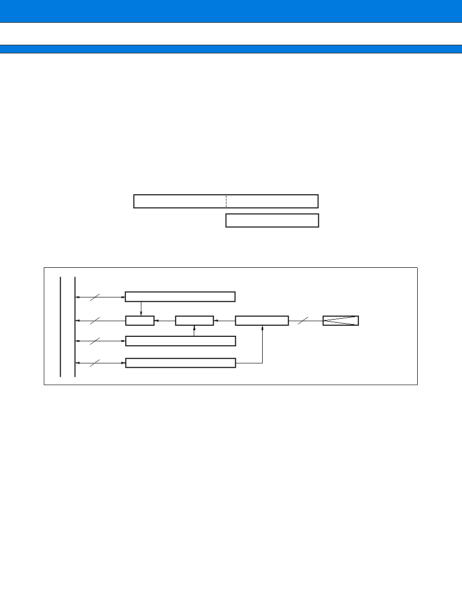
43
MB90230 Series
9. DTP/External Interrupt
The data transfer peripheral (DTP) is located between external peripherals and the F
2
MC-16F CPU. It receives
a DMA request or interrupt request generated by the external peripherals and reports it to the F
2
MC-16F CPU
to activate the extended intelligent I/O service or interrupt handler. The user can select two request levels of
"H" and "L" for extended intelligent I/O service (EI
2
OS) or, four request levels of "H," "L," rising edge, and falling
edge for external interrupt requests.
(1) Register Configuration
(2) Block Diagram
EIRR
ENIR
Interrupt/DTP enable register
000031
H
, 30
H
ELVR
Request level setting register
000032
H
15
8
7
0
bit
Address:
4
Gate
4
Source F/F
Edge detection circuit
3
Interrupt DTP source register
4
Request level setting register
8
Request input
F
2
MC-16 bus
Interrupt DTP source register
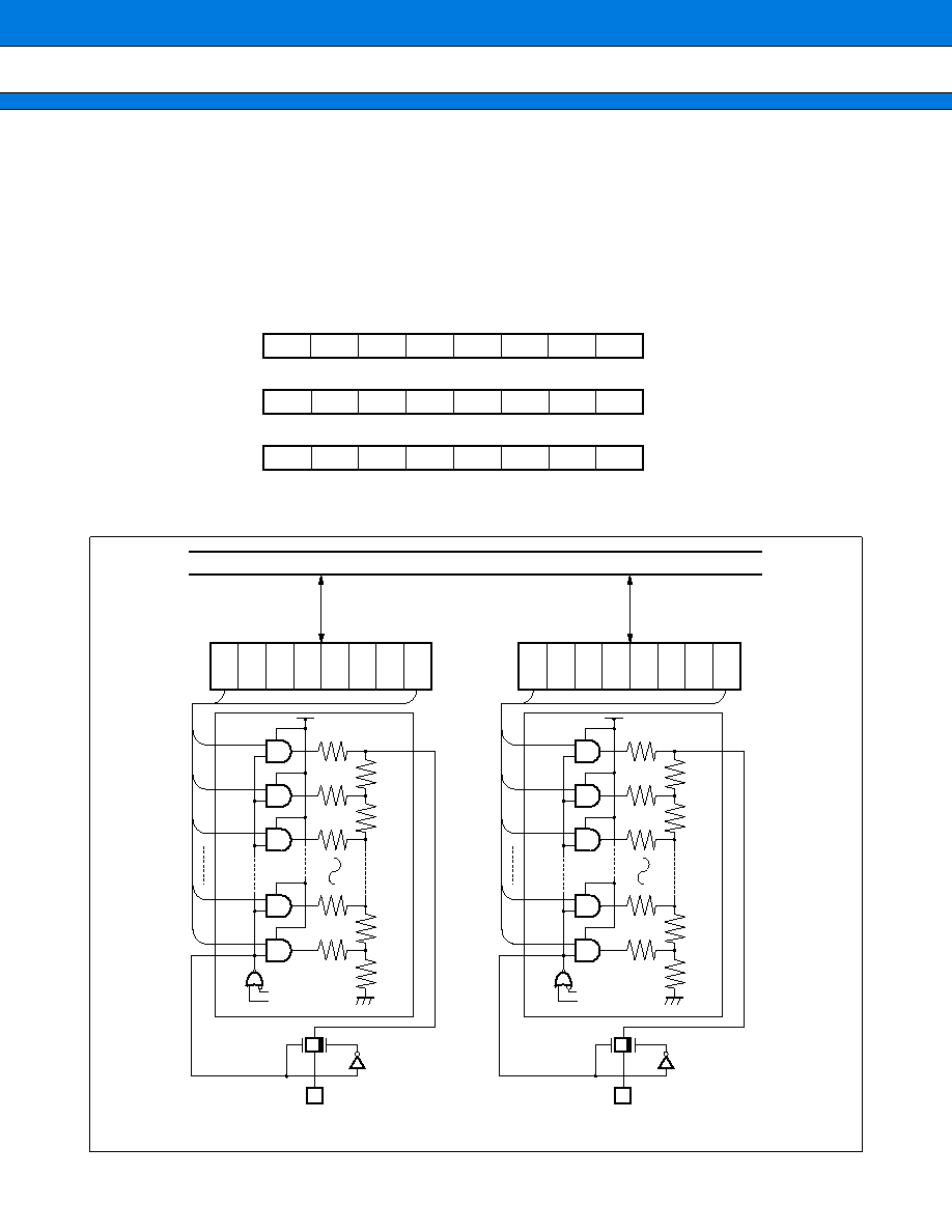
MB90230 Series
44
10.
D/A Converter
This block is an R-2R type D/A converter with 8-bit resolution.
The D/A converter incorporates two channels, each of which can be controlled for output independently by the
D/A control register.
(1) Register Configuration
(2) Block Diagram
DA17
DA16
DA15
DA14
DA13
DA12
DA11
DA10
15
14
13
12
11
10
9
8
DA07
DA06
DA05
DA04
DA03
DA02
DA01
DA00
7
6
5
4
3
2
1
0
--
--
--
--
--
--
DAE1
DAE0
7
6
5
4
3
2
1
0
DAT1
Address: 00003D
H
DAT0
Address: 00003C
H
DACR
Address: 00003E
H
D/A converter data register 1
D/A converter data register 2
D/A control register
bit
F
2
MC-16 bus
DA
17
DA
16
DA
15
DA
14
DA
13
DA
12
DA
11
DA
10
DA
07
DA
06
DA
05
DA
04
DA
03
DA
02
DA
01
DA
00
DAE1
Standby control
2R
2R
2R
2R
R
R
R
AV
CC
DA17
DA16
DA15
DA11
DA10
DA output
ch. 1
DAE0
Standby control
2R
2R
2R
2R
R
R
R
AV
CC
DA07
DA06
DA05
DA01
DA00
DA output
ch. 0
2R
2R

45
MB90230 Series
11.
Level Comparator
This module compares the input level (by checking whether it is high or low).
The module consists of a comparator, 4-bit resistor ladder, and control register.
∑ The external input can be compared to the internal 4-bit resistor ladder.
(1) Register Configuration
(2) Block Diagram
LVLC
8
0
Level comparator
00002F
H
bit
Address:
RD3
RD2
RD1
RD0
CPLV
INT
INTE
CPEN
Resistor ladder
Bus
AVRH
AVRL
4
4-bit D/A
S/H
CMP
Comparator
Analog input
Interrupt

MB90230 Series
46
12.Watchdog Timer and Timebase Timer
The watchdog timer consists of a 2-bit watchdog counter using carry signals from an 18-bit timebase counter
as the clock source, a control register, and a watchdog reset control section. The timebase timer consists of
an 18-bit timer and an interval interrupt control circuit.
(1) Register Configuration
(2) Block Diagram
TBTC
WTC
15
8
7
0
Timebase timer control register
0000A9
H
, A8
H
Address:
bit
TBTC
TBC1
TBC0
TBR
TBIE
TBOF
Selector
AND
Q
R
S
Selector
Timebase
interrupt
WTC
WT1
WT0
WTE
PONR
STBR
WRST
ERST
SRST
From RST bit in STBYC register
RST pin
From hardware standby
control circuit
From power-on occurrence
WDGRST
To internal reset generator
2-bit counter
OF
CLR
Watchdog reset
generator
CLR
2
12
2
14
2
16
2
18
TBTRES
Clock input
Timebase timer
2
14
2
16
2
17
2
18
Oscillation clock
F
2
MC-16 bus
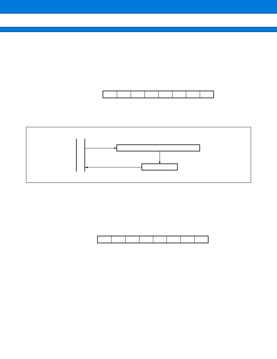
47
MB90230 Series
13. Delay Interruupt Generation Module
The delayed interrupt generation module is used to generate an interrupt for task switching. Using this module
allows an interrupt request to the F
2
MC-16F CPU to be generated or canceled by software.
(1) Register Configuration
(2) Block Diagram
14.
Clock Output Control Register
The clock output control register outputs the output from the communication prescaler to the pin.
(1) Register Configuration
--
--
--
--
--
--
--
R0
15
14
13
12
11
10
9
8
Address: 00009F
H
DIRR
Read/write
Initial value
Delayed interrupt source
generate/release register
(--)
(X)
(--)
(X)
(--)
(X)
(--)
(X)
(--)
(X)
(--)
(X)
(--)
(X)
(R/W)
(0)
bit
Interrupt source latch
Delayed interrupt source generate/release decoder
F
2
MC-16 bus
--
--
--
--
--
CKEN
FRQ1
FRQ0
15
14
13
12
11
10
9
8
Address: 00002E
H
CLKR
Read/write
Initial value
Clock control register
(--)
(--)
(--)
(--)
(--)
(--)
(--)
(--)
(--)
(--)
(R/W)
(0)
(R/W)
(0)
(R/W)
(0)
bit
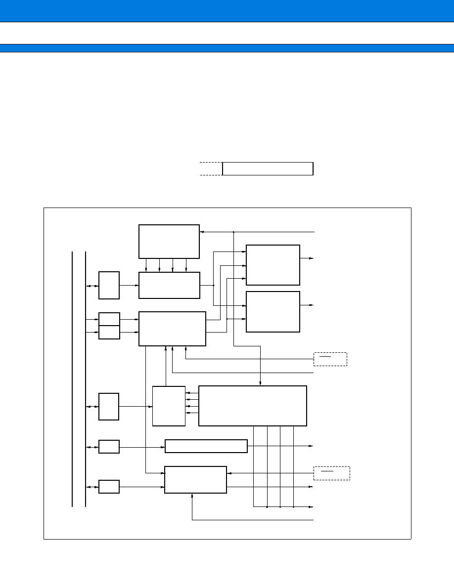
MB90230 Series
48
15.Low-power Consumption Control Circuit
The low-power consumption control circuit consists of a low-power consumption control register, clock generator,
standby status control circuit, and gear divider circuit. These internal circuits implements the sleep, stop, and
hardware standby modes as well as the clock gear function. The gear function allows the machine clock cycle
to be selected as a division of the frequency of crystal oscillation or external clock input by 1, 2, 4, or 16.
(1) Register Configuration
(2) Block Diagram
STBYC
15
8
7
0
Standby control register
Address: 0000A0
H
bit
Selector
2
14
2
0
Selector
Gear divider circuit
1/1 1/2 1/4 1/16
STBYC
CLK1
CLK0
SLP
STP
OSC1
OSC0
SPL
RST
Internal reset generator
WDGRST
To watchdog timer
Internal RST
RST pin
Standby control circuit
RST
Clear HST start
Pin high-impedance control circuit
Pin HI-Z
HST pin
Interrupt request or RST
2
16
2
17
2
18
Clock input
Time-base timer
2
16
2
17
2
18
Resource clock
generator
CPU clock
generator
Resource clock
CPU clock
Oscillation clock
F
2
MC-16 bus
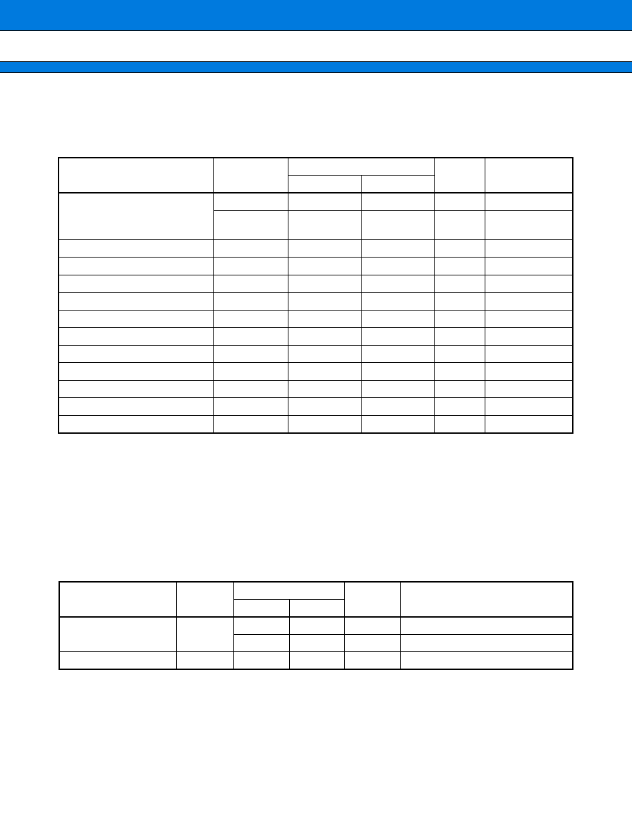
49
MB90230 Series
s
ELECTRICAL CHARACTERISTICS
1. Absolute Maximum Ratings
(V
SS
= 0.0 V)
*1: AVRH, AVRL, or AV
CC
must not exceed V
CC
.
AV
SS
and AVRH must not exceed AVRH and AV
CC
, respectively.
V
CC
AV
CC
AVRH > AVRL
AV
SS
V
SS
*2: V
I
or V
O
must not exceed "V
CC
+ 0.3 V."
WARNING: Permanent device damage may occur if the above "Absolute Maximum Ratings" are exceeded.
Functional operation should be restricted to the conditions as detailed in the operational sections of
this data sheet. Exposure to absolute maximum rating conditions for externded periods may affect
device reliability.
2. Recommended Operating Conditions
(V
SS
= 0.0 V)
Parameter
Symbol
Value
Unit
Remarks
Min.
Max.
Power supply voltage
V
CC
V
SS
≠ 0.3
V
SS
+ 7.0
V
AV
CC
, AV
SS
AVRH, AVRL
V
CC
≠ 0.3*
1
V
SS
+ 7.0
V
Input voltage
V
I
*
2
V
SS
≠ 0.3
V
CC
+ 0.3
V
Output voltage
V
O
*
2
V
SS
≠ 0.3
V
CC
+ 0.3
V
"L" level output current
I
OL
20
mA
"L" level average output current
I
OLAV
--
4
mA
"L" level total output current
I
OL
50
mA
"H" level output current
I
OH
≠10
mA
"H" level average output current
I
OHAV
--
≠4
mA
"H" level total output current
I
OH
--
≠50
mA
Power consumption
P
D
--
400
mW
Operating temperature
T
A
≠40
+70
∞
C
Storage temperature
T
STG
≠55
+150
∞
C
Parameter
Symbol
Value
Unit
Remarks
Min.
Max.
Power supply voltage
V
CC
4.75
5.25
V
During normal operation
3.0
5.5
V
In stop mode
Operating temperature
T
A
≠40
+70
∞
C

MB90230 Series
50
3. DC Characteristics
(V
CC
= 5.0 V
±
5%, V
SS
= 0.0 V, T
A
= ≠40
∞
C to +70
∞
C)
*1: CMOS I/O pin (Other than hysteresis pins)
*2: Hysteresis input pins: P46/TRG, P70/ATG, P71/ESI, P80/INT0, P81/INT1, P82/OUT0/INT2, P83/OUT1/INT3,
P90/IN0, P91/IN1, P92/IN2, P93/IN3/CKOT, P94/SIN0, P96/SCK0, PA0/SIN1,
PA2/SCK1, PA3/SIN2, PA5/SCK2
*3: Mode pins MD2 to MD0
*4: Open-drain pins P94 to P96 and PA0 to PA5: Set by registers
*5: Pins with pull-up resistor RST and P00 to P27: Set by registers
Parameter
Symbol
Pin
name
Condition
Value
Unit
Remarks
Min.
Typ.
Max.
"H" level input
voltage
V
IH
*1
V
CC
= 5.0 V
±
5%
0.7 V
CC
--
V
CC
+ 0.3
V
V
IHS
*2
0.8 V
CC
--
V
CC
+ 0.3
V
Hysteresis input
V
IHM
*3
V
CC
≠ 0.3
--
V
CC
+ 0.3
V
MD0 to 2
"L" level input
voltage
V
IL
*1
V
CC
= 5.0 V
±
5%
V
SS
≠ 0.3
--
0.3 V
CC
V
V
ILS
*2
V
SS
≠ 0.3
--
0.2 V
CC
V
Hysteresis input
V
ILM
*3
V
SS
≠ 0.3
--
V
SS
+ 0.3
V
MD0 to 2
"H" level output
voltage
V
OH
*1, *2
V
CC
= 4.75 V
I
OH
= ≠2.0 mA
2.4
--
--
V
"L" level output
voltage
V
OL
*1, *2
V
CC
= 4.75 V
I
OL
= 1.8 mA
--
--
0.4
V
Input leakage
current
I
IH
*1, *2,
*3
V
SS
+ 4.75 V
<V
I
<V
CC
≠10
--
10
µ
A
Power supply
current
I
CC
V
CC
V
CC
= 5.0 V
±
5%
fc = 16 MHz
--
48
80
mA
I
CCS
--
15
25
mA In sleep mode
I
CCH
--
10
--
µ
A
In stop mode
Input capacity
C
IN
Other
than V
CC
and V
SS
--
--
10
--
pF
Open-drain
output leakage
current
(N-channel Tr
OFF)
I
LEAK
*4
--
--
0.1
10
µ
A
Pull-up current
I
PULL
*5
--
≠250
--
≠50
µ
A

51
MB90230 Series
4. AC Characteristics
(1) Clock Timing Standards
(V
CC
= +5.0 V
±
5%, V
SS
= 0.0 V, T
A
= ≠40
∞
C to +70
∞
C)
Parameter
Symbol
Pin name
Condition
Value
Unit
Remarks
Min.
Max.
Clock frequency
f
C
X0
X1
V
CC
= 5.0 V
±
5%
1
16
MHz
Clock cycle time
t
C
X0
X1
V
CC
= 5.0 V
±
5%
62.5
--
ns
Input clock pulse width
P
WH
P
WL
X0
V
CC
= 5.0 V
±
5%
25.0
--
ns
Duty = 60%
Input clock rising/falling
time
t
cr
t
cf
X0
--
5
10
ns
P
WH
P
WL
t
cf
t
cr
t
c
0.8 V
CC
0.2 V
CC
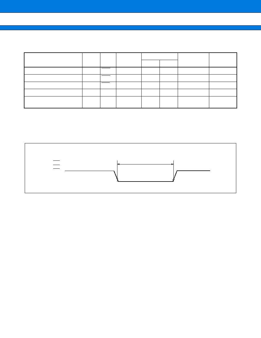
MB90230 Series
52
(2) Reset, Hardware Standby, and Trigger Input Standards
(V
CC
= +5.0 V
±
5%, V
SS
= 0.0 V, T
A
= ≠40
∞
C to +70
∞
C)
*Machine cycle: t
CYC
= 1/machine clock = 1/(f
C
˜
N)
f
C
: Oscillation frequency
N: Gear divide ratio (1, 2, 4, 16)
Note: Clock input is required during reset.
The machine cycle at hardware standby input is set to 1/32 divided oscillation.
Parameter
Symbol
Pin
name
Condition
Value
Unit
Remarks
Min.
Max.
Reset input time
t
RSTL
RST
--
5
--
Machine cycle*
Hardware standby input time t
HSTL
HST
--
5
--
Machine cycle*
A/D start trigger input time
t
ATGX
ATG
--
5
--
Machine cycle*
PPG start trigger input time
t
PPGL
TRG
--
5
--
Machine cycle*
Input capture input trigger
t
INP
IN0 to
IN3
--
5
--
Machine cycle*
t
RSTL
, t
HSTL
, t
INP
t
ATGX
, t
PPGT
RST
HST
ATG
TRG
IN0 to IN3

53
MB90230 Series
(3) Power-on Reset
(V
CC
= +5.0 V
±
5%, V
SS
= 0.0 V, T
A
= ≠40
∞
C to +70
∞
C)
Parameter
Symbol
Pin name
Condition
Value
Unit
Remarks
Min.
Max.
Power supply riseing time
t
R
V
cc
--
--
50
ms
Power-off time
t
OFF
1
--
ms
V
cc
t
R
4.5 V
0.2 V
t
OFF
Vcc
5 V
3 V
Vss
RAM data refined
It is recommended to keep the
rising speed of the supply voltage
at 50 mV/ms or slower.
Keep in mind that abrupt changes in supply voltage may cause a power-on reset.

MB90230 Series
54
(4) UART Timing
(V
CC
= +5.0 V
±
5%, V
SS
= 0.0 V, T
A
= ≠40
∞
C to +70
∞
C)
Notes: ∑ These AC characteristics assume the CLK synchronous mode.
∑ C
L
is the value for load capacity applied to the pin under testing.
∑ t
CYC
is the machine cycle (in nanoseconds).
Parameter
Symbol
Pin
name
Condition
Value
Unit
Remarks
Min.
Max.
Serial clock cycle time
t
SCYC
--
Internal clock
operation output
pin: C
L
= 80 pF
8 t
CYC
--
ns
SCK
SOT delay time
t
SLOV
--
≠80
80
ns
Valid SIN
SCK
t
IVSH
--
100
--
ns
SCK
Valid SIN hold time
t
SHIX
--
60
--
ns
Serial clock "H" pulse width
t
SHSL
--
External clock
operation output
pin: C
L
= 80 pF
4 t
CYC
--
ns
Serial clock "L" pulse width
t
SLSH
--
4 t
CYC
--
ns
SCK
SOT delay time
t
SLOV
--
--
150
ns
Valid SIN
SCK
t
IVSH
--
60
--
ns
SCK
Valid SIN hold time
t
SHIX
--
60
--
ns
SOT
SCK
SIN
t
SLOV
t
SCYC
t
IVSH
t
SHIX
SOT
SCK
SIN
t
SLOV
t
SLSH
t
IVSH
t
SHIX
t
SHSL
0.8 V
2.4 V
0.8 V
2.4 V
0.8 V
2.4 V
0.8 V
2.4 V
0.8 V
2.4 V
0.8 V
0.8 V
2.4 V
2.4 V
0.8 V
2.4 V
0.8 V
2.4 V
0.8 V
∑ Internal shift clock mode
∑ External shift clock mode
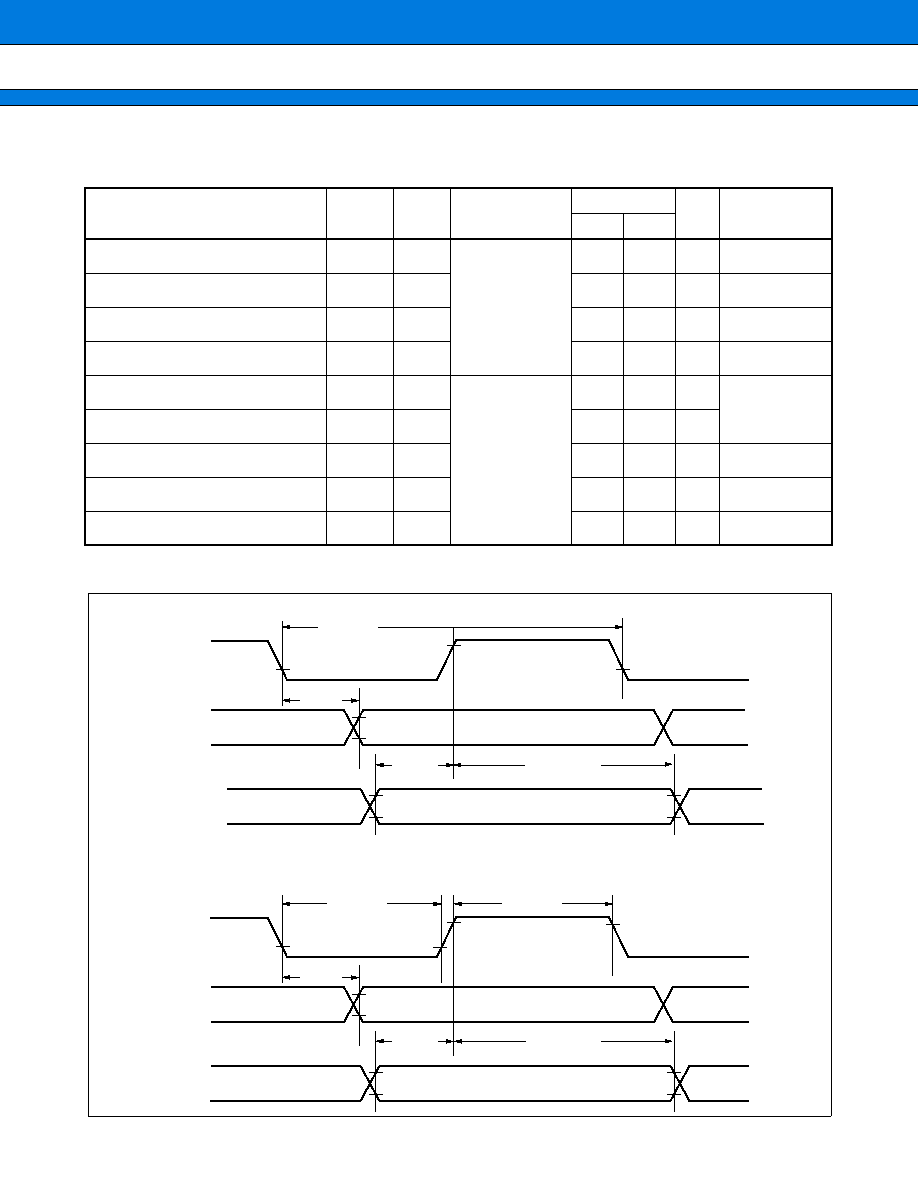
55
MB90230 Series
(5) Extended Serial I/O Timing
(V
CC
= +5.0 V
±
5%, V
SS
= 0.0 V, T
A
= ≠40
∞
C to +70
∞
C)
Notes: ∑ C
L
is the value for load capacity applied to the pin under testing.
∑ t
CYC
is the machine cycle (in nanoseconds).
Parameter
Symbol
Pin
name
Condition
Value
Unit
Remarks
Min.
Max.
Serial clock cycle time
t
SCYC
--
Internal clock
operation output
pin: C
L
= 80 pF
8 t
CYC
--
ns
SCK
SOT delay time
t
SLOV
--
50
--
ns
Valid SIN
SCK
t
IVSH
--
1 t
CYC
--
ns
SCK
Valid SIN hold time
t
SHIX
--
1 t
CYC
--
ns
Serial clock "H" pulse width
t
SHSL
--
External clock
operation output
pin: C
L
= 80 pF
250
--
ns
External clock:
2 MHz max.
Serial clock "L" pulse width
t
SLSH
--
250
--
ns
SCK
SOT delay time
t
SLOV
--
2 t
CYC
--
ns
Valid SIN
SCK
t
IVSH
--
1 t
CYC
--
ns
SCK
Valid SIN hold time
t
SHIX
--
2 t
CYC
--
ns
SOT
SCK
SIN
t
SLOV
t
SCYC
t
IVSH
t
SHIX
SOT
SCK
SIN
t
SLOV
t
SLSH
t
IVSH
t
SHIX
t
SHSL
0.8 V
2.4 V
0.8 V
2.4 V
0.8 V
2.4 V
0.8 V
2.4 V
0.8 V
2.4 V
0.8 V
0.8 V
2.4 V
2.4 V
0.8 V
2.4 V
0.8 V
2.4 V
0.8 V
∑ Internal shift clock mode
∑ External shift clock mode
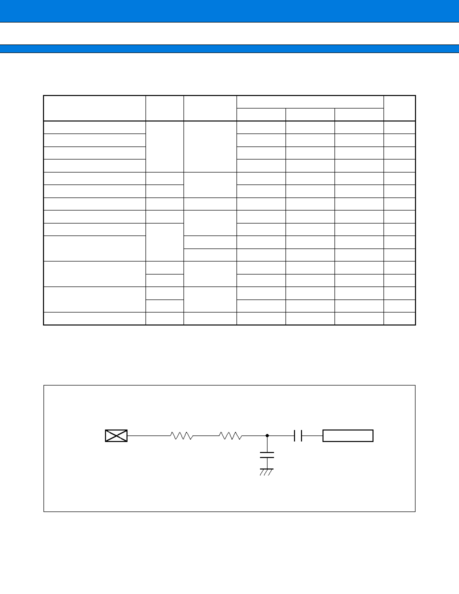
MB90230 Series
56
5. A/D Converter Electrical Characteristics
(AV
CC
= V
CC
= +5.0 V
±
5%, AV
SS
= V
SS
= 0.0 V, +3.0 V
AVRH ≠ AVRL, T
A
= ≠40
∞
C to +70
∞
C)
* : Current applied in CPU stop mode with the A/D converter inactive (V
CC
= AV
CC
= AVRH = 5.5 V).
Notes: ∑ The error becomes larger as |AVRH≠AVRL| becomes smaller.
∑ Use the output impedance of the external circuit for analog input under the following conditions: External
circuit output impedance < Approx. 7 k
∑ If the output impedance the external circuit is too high, the analog voltage sampling time may be insufficient.
(Sampling time = 3.0
µ
s at a machine clock frequency of 16 MHz)
Parameter
Symbol
Pin name
Value
Unit
Min.
Typ.
Max.
Resolution
--
--
--
10
10
bit
Total error
--
--
±
3.0
LSB
Linearity error
--
--
±
2.0
LSB
Differential linearity error
--
--
±
1.5
LSB
Zero transition voltage
V
OT
AN0 to AN7
≠1.5
+0.5
+2.5
LSB
Full-scale transition voltage
V
FST
AVRH ≠4.5
AVRH ≠1.5
AVRH +0.5
LSB
Conversion time
--
f
C
= 16 MHz
5.00
--
--
µ
s
Analog port input current
I
AIN
AN0 to AN7
--
--
10
µ
A
Analog input voltage
--
AVRL
--
AVRH
V
Reference voltage
AVRH
AVRL
--
AV
CC
V
AVRL
0
--
AVRH
V
Power supply current
I
A
AV
CC
--
5
--
mA
I
AS
--
--
5*
µ
A
Reference voltage supply
current
I
R
AVRH
--
200
--
µ
A
I
RS
--
--
5*
µ
A
Variation between channels
--
AN0 to AN7
--
--
4
LSB
Note: The values shown here are reference values.
Analog input
Comparator
C
1
C
0
R
ON2
R
ON1
R
ON2
+ R
ON2
= Approx. 3 k
C
0
= Approx. 60 pF
C
1
= Approx. 4 pF
∑ Analog Input Circuit Mode
57
MB90230 Series
6. A/D Glossary
∑ Resolution
Analog changes that are identifiable with the A/D converter.
When the number of bits is 10, analog voltage can be divided into 2
10
= 1024
∑ Total error
Difference between actual and logical values. This error is caused by a zero transition error, full-scale transition
error, linearity error, differential linearity error, or by noise.
∑ Linearity error
The deviation of the straight line connecting the zero transition point ("00 0000 0000"
"00 0000 0001") with
the full-scale transition point ("11 1111 1111"
"11 1111 1110") from actual conversion characteristics
∑ Differential linearity error
The deviation of input voltage needed to change the output code by 1 LSB from the theoretical value
Analog input
V
FST
Linearity error
Digital output
11 1111 1111
11 1111 1110
∑
∑
∑
∑
∑
∑
∑
∑
∑
∑
∑
00 0000 0010
00 0000 0001
00 0000 0000
V
OT
V
NT
V
(N+1)T
(1LSB
◊
N + V
OT
)
1LSB
1022
Linearity error
-
1
V
FST
-
V
OT
V
NT
-
(1LSB
◊
N + V
OT
)
V
( N+1)T
-
V
NT
1LSB
1LSB
(LSB)
(LSB)
Differential linearity error =
=
=
MB90230 Series
58
7. D/A Converter Electrical Characteristics
(AV
CC
= V
CC
= +5.0 V
±
5%, AV
SS
= V
SS
= 0.0 V, T
A
= ≠40
∞
C to +70
∞
C)
*: A load capacity of 20 pF is assumed.
Parameter
Symbol
Pin name
Value
Unit
Min.
Typ.
Max.
Resolution
--
--
--
8
8
bit
Differential linearity error
--
--
--
--
±
0.9
LSB
Conversion time
--
--
--
10*
20*
µ
s
Analog output impedance
--
--
--
28
--
K
59
MB90230 Series
8. Serial E
2
PROM Interface Timing
(1) E
2
PROM interface at an operation clock frequency of 1 MHz
(V
CC
= +5.0 V
±
5%, V
SS
= 0.0 V, T
A
= ≠40
∞
C to +70
∞
C)
(2) E
2
PROM interface at an operation clock frequency of 2 MHz
(V
CC
= +5.0 V
±
5%, V
SS
= 0.0 V, T
A
= ≠40
∞
C to +70
∞
C)
Parameter
Symbol
Value
Unit
Remarks
Min.
Typ.
Max.
Operation cycle
t
SK
1.0
--
--
µ
s
Clock "H" time
t
SKH
0.4
0.5
--
µ
s
Clock "L" time
t
SKL
0.4
0.5
--
µ
s
ECS setup time
t
CSS
0.3
--
--
µ
s
ECS hold time
t
CSH
0.0
--
--
µ
s
EDO data decision time
t
PD
0.3
--
--
µ
s
EDO output hold time
t
OH
0.5
--
--
µ
s
EDI setup time
t
DIS
0.0
--
--
µ
s
EDI hold time
t
DIH
0.4
--
--
µ
s
READY
ECS
t
RCSH
0.4
--
--
µ
s
ECS "L" time
t
CSL
0.8
1.0
--
µ
s
Parameter
Symbol
Value
Unit
Remarks
Min.
Typ.
Max.
Operation cycle
t
SK
0.5
--
--
µ
s
Clock "H" time
t
SKH
0.2
0.25
--
µ
s
Clock "L" time
t
SKL
0.2
0.25
--
µ
s
ECS setup time
t
CSS
0.15
--
--
µ
s
ECS hold time
t
CSH
0.0
--
--
µ
s
EDO data decision time
t
PD
0.15
--
--
µ
s
EDO output hold time
t
OH
0.25
--
--
µ
s
EDI setup time
t
DIS
0.0
--
--
µ
s
EDI hold time
t
DIH
0.2
--
--
µ
s
READY
ECS
t
RCSH
0.2
--
--
µ
s
ECS "L" time
t
CSL
0.4
0.5
--
µ
s
MB90230 Series
60
EDO
ESK
ECS
t
SK
t
SKH
Determined data
Determined data
t
PD
t
CSH
EDI
t
DIS
t
CSS
Input data
Input data
ECS
DO
(E
2
PROM output)
BUSY
READY
Hi-z
MB90230 series
E
2
PROM
ECS
ESK
EDO
EDI
ECS
ESK
EDI
EDO
t
DIH
t
ST
t
CSL
t
SKL
t
OH
61
MB90230 Series
s
INSTRUCTIONS (412 INSTRUCTIONS)
Table 1 Description of Instruction Table
Item
Description
Mnemonic
Upper-case letters and symbols: Described directry in assembly code
Lower-case letters: Replaced when described in assembly code
Numbers after lower-case letters: Indicates the bit width within the code
#
Indicates the number of bytes
~
Indicates the number of cycles
See Table 4 for details about meanings of letters in items.
B
Indicates the compensation value for calculating the number of actual cycles during
execution of instruction.
The number of actual cycles during execution of instruction is summed with the value in
the "cycles" column.
Operation
Indicates operation of instruction.
LH
Indicates special operations involving the bits 15 through 08 of the accumulator.
Z: Transfers "0"
X: Extends before transferring
--: No transfer
AH
Indicates special operations involving the high-order 16 bits in the accumulator.
*: Transfers from AL to AH
--: No transfer
Z: Transfers 00
H
to AH.
X: Transfers 00
H
or FF
H
to AH by extending AL
I
Indicates the status of each of the following flags: I (interrupt enable), S (stack), T (sticky
bit), N (negative), Z (zero), V (overflow), and C (carry).
*: Changes due to execution of instruction.
--: No change.
S: Set by execution of instruction.
R: Reset by execution of instruction.
S
T
N
Z
V
C
RMW
Indicates whether the instruction is a read-modify-write instruction (a single instruction
that reads data from memory, etc., processes the data, and then writes the result to
memory.).
*: Instruction is a read-modify-write instruction
--: Instruction is not a read-modify-write instruction
Note: Cannot be used for addresses that have different meanings depending on
whether they are read or written.
MB90230 Series
62
Table 2 Explanation of Symbols in Table of Instructions
Symbol
Description
A
32-bit accumulator
The number of bits used varies according to the instruction.
Byte: Low order 8 bits of AL
Word: 16 bits of AL
Long: 32 bits of AL, AH
AH
High-order 16 bits of A
AL
Low-order 16 bits of A
SP
Stack pointer (USP or SSP)
PC
Program counter
SPCU
Stack pointer upper limit register
SPCL
Stack pointer lower limit register
PCB
Program bank register
DTB
Data bank register
ADB
Additional data bank register
SSB
System stack bank register
USB
User stack bank register
SPB
Current stack bank register (SSB or USB)
DPR
Direct page register
brg1
DTB, ADB, SSB, USB, DPR, PCB, SPB
brg2
DTB, ADB, SSB, USB, DPR, SPB
Ri
R0, R1, R2, R3, R4, R5, R6, R7
RWi
RW0, RW1, RW2, RW3, RW4, RW5, RW6, RW7
RWj
RW0, RW1, RW2, RW3
RLi
RL0, RL1, RL2, RL3
dir
addr16
addr24
addr24 0 to 15
addr24 16 to 23
Compact direct addressing
Direct addressing
Physical direct addressing
Bits 0 to 15 of addr24
Bits 16 to 23 of addr24
io
I/O area (000000
H
to 0000FF
H
)
#imm4
#imm8
#imm16
#imm32
ext (imm8)
4-bit immediate data
8-bit immediate data
16-bit immediate data
32-bit immediate data
16-bit data signed and extended from 8-bit immediate data
disp8
disp16
8-bit displacement
16-bit displacement
bp
Bit offset value
vct4
vct8
Vector number (0 to 15)
Vector number (0 to 255)
( )b
Bit address
rel
ear
eam
Branch specification relative to PC
Effective addressing (codes 00 to 07)
Effective addressing (codes 08 to 1F)
rlst
Register list
63
MB90230 Series
Table 3 Effective Address Fields
* : The number of bytes for address extension is indicated by the "+" symbol in the "#" (number of bytes) column in
the Table of Instructions.
Code
Notation
Address format
Number of bytes in
address extemsion*
00
01
02
03
04
05
06
07
R0
R1
R2
R3
R4
R5
R6
R7
RW0
RW1
RW2
RW3
RW4
RW5
RW6
RW7
RL0
(RL0)
RL1
(RL1)
RL2
(RL2)
RL3
(RL3)
Register direct
"ea" corresponds to byte, word, and
long-word types, starting from the
left
--
08
09
0A
0B
@RW0
@RW1
@RW2
@RW3
Register indirect
0
0C
0D
0E
0F
@RW0 +
@RW1 +
@RW2 +
@RW3 +
Register indirect with post-increment
0
10
11
12
13
14
15
16
17
@RW0 + disp8
@RW1 + disp8
@RW2 + disp8
@RW3 + disp8
@RW4 + disp8
@RW5 + disp8
@RW6 + disp8
@RW7 + disp8
Register indirect with 8-bit
displacement
1
18
19
1A
1B
@RW0 + disp16
@RW1 + disp16
@RW2 + disp16
@RW3 + disp16
Register indirect with 16-bit
displacemen
2
1C
1D
1E
1F
@RW0 + RW7
@RW1 + RW7
@PC + dip16
addr16
Register indirect with index
Register indirect with index
PC indirect with 16-bit displacement
Direct address
0
0
2
2

MB90230 Series
64
Table 4 Number of Execution Cycles for Each Form of Addressing
* : "(a)" is used in the "cycles" (number of cycles) column and column B (correction value) in the Table of Instructions.
Table 5 Correction Values for Number of Cycles Used to Calculate Number of Actual Cycles
* : "(b)", "(c)", and "(d)" are used in the "cycles" (number of cycles) column and column B (correction value) in the
Table of Instructions.
Code
Operand
(a)*
Number of execution cycles for each from of addressing
00 to 07
Ri
RWi
RLi
Listed in Table of Instructions
08 to 0B
@RWj
1
0C to 0F
@RWj +
4
10 to 17
@RWi + disp8
1
18 to 1B
@RWj + disp16
1
1C
1D
1E
1F
@RW0 + RW7
@RW1 + RW7
@PC + dip16
@addr16
2
2
2
1
Operand
(b)*
(c)*
(d)*
byte
word
long
Internal register
+
0
+
0
+
0
Internal RAM even address
+
0
+
0
+
0
Internal RAM odd address
+
0
+
1
+
2
Even address not in internal RAM
+
1
+
1
+
2
Odd address not in internal RAM
+
1
+
3
+
6
External data bus (8 bits)
+
1
+
3
+
6
65
MB90230 Series
Table 6 Transfer Instructions (Byte) [50 Instructions]
For an explanation of "(a)" and "(b)", refer to Table 4, "Number of Execution Cycles for Each Form of Addressing,"
and Table 5, "Correction Values for Number of Cycles Used to Calculate Number of Actual Cycles."
Mnemonic
#
~
B
Operation
LH AH
I
S
T
N
Z
V
C
RMW
MOV
A, dir
MOV
A, addr16
MOV
A, Ri
MOV
A, ear
MOV
A, eam
MOV
A, io
MOV
A, #imm8
MOV
A, @A
MOV
A, @RLi+disp8
MOV
A, @SP+disp8
MOVP
A, addr24
MOVP
A, @A
MOVN A, #imm4
MOVX
A, dir
MOVX
A, addr16
MOVX
A, Ri
MOVX
A, ear
MOVX
A, eam
MOVX
A, io
MOVX
A, #imm8
MOVX
A, @A
MOVX
A,@RWi+disp8
MOVX
A, @RLi+disp8
MOVX
A, @SP+disp8
MOVPX A, addr24
MOVPX A, @A
MOV
dir, A
MOV
addr16, A
MOV
Ri, A
MOV
ear, A
MOV
eam, A
MOV
io, A
MOV
@RLi+disp8, A
MOV
@SP+disp8, A
MOVP
addr24, A
MOV
Ri, ear
MOV
Ri, eam
MOVP
@A, Ri
MOV
ear, Ri
MOV
eam, Ri
MOV
Ri, #imm8
MOV
io, #imm8
MOV
dir, #imm8
MOV
ear, #imm8
MOV
eam, #imm8
MOV
@AL, AH
XCH
A, ear
XCH
A, eam
XCH
Ri, ear
XCH
Ri, eam
2
3
1
2
2+
2
2
2
3
3
5
2
1
2
3
2
2
2+
2
2
2
2
3
3
5
2
2
3
1
2
2+
2
3
3
5
2
2+
2
2
2+
2
3
3
3
3+
2
2
2+
2
2+
2
2
1
1
2+ (a)
2
2
2
6
3
3
2
1
2
2
1
1
2+ (a)
2
2
2
3
6
3
3
2
2
2
1
2
2+ (a)
2
6
3
3
2
3+ (a)
3
3
3+ (a)
2
3
3
2
2+ (a)
2
3
3+ (a)
4
5+ (a)
(b)
(b)
0
0
(b)
(b)
0
(b)
(b)
(b)
(b)
(b)
0
(b)
(b)
0
0
(b)
(b)
0
(b)
(b)
(b)
(b)
(b)
(b)
(b)
(b)
0
0
(b)
(b)
(b)
(b)
(b)
0
(b)
(b)
0
(b)
0
(b)
(b)
0
(b)
(b)
0
2
◊
(b)
0
2
◊
(b)
byte (A)
(dir)
byte (A)
(addr16)
byte (A)
(Ri)
byte (A)
(ear)
byte (A)
(eam)
byte (A)
(io)
byte (A)
imm8
byte (A)
((A))
byte (A)
((RLi))+disp8)
byte (A)
((SP)+disp8)
byte (A)
(addr24)
byte (A)
((A))
byte (A)
imm4
byte (A)
(dir)
byte (A)
(addr16)
byte (A)
(Ri)
byte (A)
(ear)
byte (A)
(eam)
byte (A)
(io)
byte (A)
imm8
byte (A)
((A))
byte (A)
((RWi))+disp8)
byte (A)
((RLi))+disp8)
byte (A)
((SP)+disp8)
byte (A)
(addr24)
byte (A)
((A))
byte (dir)
(A)
byte (addr16)
(A)
byte (Ri)
(A)
byte (ear)
(A)
byte (eam)
(A)
byte (io)
(A)
byte ((RLi)) +disp8)
(A)
byte ((SP)+disp8)
(A)
byte (addr24)
(A)
byte (Ri)
(ear)
byte (Ri)
(eam)
byte ((A))
(Ri)
byte (ear)
(Ri)
byte (eam)
(Ri)
byte (Ri)
imm8
byte (io)
imm8
byte (dir)
imm8
byte (ear)
imm8
byte (eam)
imm8
byte ((A))
(AH)
byte (A)
(ear)
byte (A)
(eam)
byte (Ri)
(ear)
byte (Ri)
(eam)
Z
Z
Z
Z
Z
Z
Z
Z
Z
Z
Z
Z
Z
X
X
X
X
X
X
X
X
X
X
X
X
X
≠
≠
≠
≠
≠
≠
≠
≠
≠
≠
≠
≠
≠
≠
≠
≠
≠
≠
≠
≠
Z
Z
≠
≠
*
*
*
*
*
*
*
≠
*
*
*
≠
*
*
*
*
*
*
*
*
≠
*
*
*
*
≠
≠
≠
≠
≠
≠
≠
≠
≠
≠
≠
≠
≠
≠
≠
≠
≠
≠
≠
≠
≠
≠
≠
≠
≠
≠
≠
≠
≠
≠
≠
≠
≠
≠
≠
≠
≠
≠
≠
≠
≠
≠
≠
≠
≠
≠
≠
≠
≠
≠
≠
≠
≠
≠
≠
≠
≠
≠
≠
≠
≠
≠
≠
≠
≠
≠
≠
≠
≠
≠
≠
≠
≠
≠
≠
≠
≠
≠
≠
≠
≠
≠
≠
≠
≠
≠
≠
≠
≠
≠
≠
≠
≠
≠
≠
≠
≠
≠
≠
≠
≠
≠
≠
≠
≠
≠
≠
≠
≠
≠
≠
≠
≠
≠
≠
≠
≠
≠
≠
≠
≠
≠
≠
≠
≠
≠
≠
≠
≠
≠
≠
≠
≠
≠
≠
≠
≠
≠
≠
≠
≠
≠
≠
≠
≠
≠
≠
≠
≠
≠
≠
≠
≠
≠
≠
≠
≠
≠
≠
≠
≠
≠
≠
≠
≠
≠
≠
≠
≠
≠
≠
≠
≠
≠
≠
*
*
*
*
*
*
*
*
*
*
*
*
R
*
*
*
*
*
*
*
*
*
*
*
*
*
*
*
*
*
*
*
*
*
*
*
*
*
*
*
*
≠
≠
*
≠
*
≠
≠
≠
≠
*
*
*
*
*
*
*
*
*
*
*
*
*
*
*
*
*
*
*
*
*
*
*
*
*
*
*
*
*
*
*
*
*
*
*
*
*
*
*
*
*
≠
≠
*
≠
*
≠
≠
≠
≠
≠
≠
≠
≠
≠
≠
≠
≠
≠
≠
≠
≠
≠
≠
≠
≠
≠
≠
≠
≠
≠
≠
≠
≠
≠
≠
≠
≠
≠
≠
≠
≠
≠
≠
≠
≠
≠
≠
≠
≠
≠
≠
≠
≠
≠
≠
≠
≠
≠
≠
≠
≠
≠
≠
≠
≠
≠
≠
≠
≠
≠
≠
≠
≠
≠
≠
≠
≠
≠
≠
≠
≠
≠
≠
≠
≠
≠
≠
≠
≠
≠
≠
≠
≠
≠
≠
≠
≠
≠
≠
≠
≠
≠
≠
≠
≠
≠
≠
≠
≠
≠
≠
≠
≠
≠
≠
≠
≠
≠
≠
≠
≠
≠
≠
≠
≠
≠
≠
≠
≠
≠
≠
≠
≠
≠
≠
≠
≠
≠
≠
≠
≠
≠
≠
≠
≠
≠
≠
≠
≠
≠
≠
≠
≠
≠
≠
≠
≠
≠
≠
MB90230 Series
66
Table 7 Transfer Instructions (Word) [40 Instructions]
Note: For an explanation of "(a)" and "(c)", refer to Table 4, "Number of Execution Cycles for Each Form of
Addressing," and Table 5, "Correction Values for Number of Cycles Used to Calculate Number of Actual
Cycles."
Mnemonic
#
~
B
Operation
LH AH
I
S
T
N
Z
V
C
RMW
MOVW A, dir
MOVW A, addr16
MOVW A, SP
MOVW A, RWi
MOVW A, ear
MOVW A, eam
MOVW A, io
MOVW A, @A
MOVW A, #imm16
MOVW A, @RWi+disp8
MOVW A, @RLi+disp8
MOVW A, @SP+disp8
MOVPW A, addr24
MOVPW A, @A
MOVW dir, A
MOVW addr16, A
MOVW SP, # imm16
MOVW SP, A
MOVW RWi, A
MOVW ear, A
MOVW eam, A
MOVW io, A
MOVW @RWi+disp8, A
MOVW @RLi+disp8, A
MOVW @SP+disp8, A
MOVPW addr24, A
MOVPW @A, RWi
MOVW RWi, ear
MOVW RWi, eam
MOVW ear, RWi
MOVW eam, RWi
MOVW RWi, #imm16
MOVW io, #imm16
MOVW ear, #imm16
MOVW eam, #imm16
MOVW @AL, AH
XCHW A, ear
XCHW A, eam
XCHW RWi, ear
XCHW RWi, eam
2
3
1
1
2
2+
2
2
3
2
3
3
5
2
2
3
4
1
1
2
2+
2
2
3
3
5
2
2
2+
2
2+
3
4
4
4+
2
2
2+
2
2+
2
2
2
1
1
2+ (a)
2
2
2
3
6
3
3
2
2
2
2
2
1
2
2+ (a)
2
3
6
3
3
3
2
3+ (a)
3
3+ (a)
2
3
2
2+ (a)
2
3
3+ (a)
4
5+ (a)
(c)
(c)
0
0
0
(c)
(c)
(c)
0
(c)
(c)
(c)
(c)
(c)
(c)
(c)
0
0
0
0
(c)
(c)
(c)
(c)
(c)
(c)
(c)
0
(c)
0
(c)
0
(c)
0
(c)
(c)
0
2
◊
(c)
0
2
◊
(c)
word (A)
(dir)
word (A)
(addr16)
word (A)
(SP)
word (A)
(RWi)
word (A)
(ear)
word (A)
(eam)
word (A)
(io)
word (A)
((A))
word (A)
imm16
word (A)
((RWi) +disp8)
word (A)
((RLi) +disp8)
word (A)
((SP) +disp8
word (A)
(addr24)
word (A)
((A))
word (dir)
(A)
word (addr16)
(A)
word (SP)
imm16
word (SP)
(A)
word (RWi)
(A)
word (ear)
(A)
word (eam)
(A)
word (io)
(A)
word ((RWi) +disp8)
(A)
word ((RLi) +disp8)
(A)
word ((SP) +disp8)
(A)
word (addr24)
(A)
word ((A))
(RWi)
word (RWi)
(ear)
word (RWi)
(eam)
word (ear)
(RWi)
word (eam)
(RWi)
word (RWi)
imm16
word (io)
imm16
word (ear)
imm16
word (eam)
imm16
word ((A))
(AH)
word (A)
(ear)
word (A)
(eam)
word (RWi)
(ear)
word (RWi)
(eam)
≠
≠
≠
≠
≠
≠
≠
≠
≠
≠
≠
≠
≠
≠
≠
≠
≠
≠
≠
≠
≠
≠
≠
≠
≠
≠
≠
≠
≠
≠
≠
≠
≠
≠
≠
≠
≠
≠
≠
≠
*
*
*
*
*
*
*
≠
*
*
*
*
*
≠
≠
≠
≠
≠
≠
≠
≠
≠
≠
≠
≠
≠
≠
≠
≠
≠
≠
≠
≠
≠
≠
≠
≠
≠
≠
≠
≠
≠
≠
≠
≠
≠
≠
≠
≠
≠
≠
≠
≠
≠
≠
≠
≠
≠
≠
≠
≠
≠
≠
≠
≠
≠
≠
≠
≠
≠
≠
≠
≠
≠
≠
≠
≠
≠
≠
≠
≠
≠
≠
≠
≠
≠
≠
≠
≠
≠
≠
≠
≠
≠
≠
≠
≠
≠
≠
≠
≠
≠
≠
≠
≠
≠
≠
≠
≠
≠
≠
≠
≠
≠
≠
≠
≠
≠
≠
≠
≠
≠
≠
≠
≠
≠
≠
≠
≠
≠
≠
≠
≠
≠
≠
≠
≠
≠
≠
≠
≠
≠
≠
≠
≠
≠
≠
≠
≠
≠
≠
≠
≠
≠
≠
≠
≠
≠
≠
≠
*
*
*
*
*
*
*
*
*
*
*
*
*
*
*
*
*
*
*
*
*
*
*
*
*
*
*
*
*
*
*
*
≠
*
≠
*
≠
≠
≠
≠
*
*
*
*
*
*
*
*
*
*
*
*
*
*
*
*
*
*
*
*
*
*
*
*
*
*
*
*
*
*
*
*
≠
*
≠
*
≠
≠
≠
≠
≠
≠
≠
≠
≠
≠
≠
≠
≠
≠
≠
≠
≠
≠
≠
≠
≠
≠
≠
≠
≠
≠
≠
≠
≠
≠
≠
≠
≠
≠
≠
≠
≠
≠
≠
≠
≠
≠
≠
≠
≠
≠
≠
≠
≠
≠
≠
≠
≠
≠
≠
≠
≠
≠
≠
≠
≠
≠
≠
≠
≠
≠
≠
≠
≠
≠
≠
≠
≠
≠
≠
≠
≠
≠
≠
≠
≠
≠
≠
≠
≠
≠
≠
≠
≠
≠
≠
≠
≠
≠
≠
≠
≠
≠
≠
≠
≠
≠
≠
≠
≠
≠
≠
≠
≠
≠
≠
≠
≠
≠
≠
≠
≠
≠
≠
≠
≠
≠
≠
≠
67
MB90230 Series
Table 8 Transfer Instructions (Long Word) [11 Instructions]
For an explanation of "(a)" and "(d)", refer to Table 4, "Number of Execution Cycles for Each Form of Addressing,"
and Table 5, "Correction Values for Number of Cycles Used to Calculate Number of Actual Cycles."
Mnemonic
#
~
B
Operation
LH AH
I
S
T
N
Z
V
C
RMW
MOVL A, ear
MOVL A, eam
MOVL A, # imm32
MOVL A, @SP + disp8
MOVPL A, addr24
MOVPL A, @A
MOVPL@A, RLi
MOVL @SP + disp8, A
MOVPL addr24, A
MOVL ear, A
MOVL eam, A
2
2+
5
3
5
2
2
3
5
2
2+
1
3+ (a)
3
4
4
3
5
4
4
2
3+ (a)
0
(d)
0
(d)
(d)
(d)
(d)
(d)
(d)
0
(d)
long (A)
(ear)
long (A)
(eam)
long (A)
imm32
long (A)
((SP) +disp8)
long (A)
(addr24)
long (A)
((A))
long ((A))
(RLi)
long ((SP) + disp8)
(A)
long (addr24)
(A)
long (ear)
(A)
long (eam)
(A)
≠
≠
≠
≠
≠
≠
≠
≠
≠
≠
≠
≠
≠
≠
≠
≠
≠
≠
≠
≠
≠
≠
≠
≠
≠
≠
≠
≠
≠
≠
≠
≠
≠
≠
≠
≠
≠
≠
≠
≠
≠
≠
≠
≠
≠
≠
≠
≠
≠
≠
≠
≠
≠
≠
≠
*
*
*
*
*
*
*
*
*
*
*
*
*
*
*
*
*
*
*
*
*
*
≠
≠
≠
≠
≠
≠
≠
≠
≠
≠
≠
≠
≠
≠
≠
≠
≠
≠
≠
≠
≠
≠
≠
≠
≠
≠
≠
≠
≠
≠
≠
≠
≠

MB90230 Series
68
Table 9 Addition and Subtraction Instructions (Byte/Word/Long Word) [42 Instructions]
For an explanation of "(a)", "(b)", "(c)" and "(d)", refer to Table 4, "Number of Execution Cycles for Each Form of
Addressing," and Table 5, "Correction Values for Number of Cycles Used to Calculate Number of Actual Cycles."
Mnemonic
#
~
B
Operation
LH AH
I
S
T
N
Z
V
C
RMW
ADD
A, #imm8
ADD
A, dir
ADD
A, ear
ADD
A, eam
ADD
ear, A
ADD
eam, A
ADDC
A
ADDC
A, ear
ADDC
A, eam
ADDDC A
SUB
A, #imm8
SUB
A, dir
SUB
A, ear
SUB
A, eam
SUB
ear, A
SUB
eam, A
SUBC
A
SUBC
A, ear
SUBC
A, eam
SUBDC A
2
2
2
2+
2
2+
1
2
2+
1
2
2
2
2+
2
2+
1
2
2+
1
2
3
2
3+ (a)
2
3+ (a)
2
2
3+ (a)
3
2
3
2
3+ (a)
2
3+ (a)
2
2
3+ (a)
3
0
(b)
0
(b)
0
2
◊
(b)
0
0
(b)
0
0
(b)
0
(b)
0
2
◊
(b)
0
0
(b)
0
byte (A)
(A) + imm8
byte (A)
(A) + (dir)
byte (A)
(A) + (ear)
byte (A)
(A) + (eam)
byte (ear)
(ear) + (A)
byte (eam)
(eam) + (A)
byte (A)
(AH) + (AL) + (C)
byte (A)
(A) + (ear) + (C)
byte (A)
(A) + (eam) + (C)
byte (A)
(AH) + (AL) + (C) (Decimal)
byte (A)
(A) ≠ imm8
byte (A)
(A) ≠ (dir)
byte (A)
(A) ≠ (ear)
byte (A)
(A) ≠ (eam)
byte (ear)
(ear) ≠ (A)
byte (eam)
(eam) ≠ (A)
byte (A)
(AH) ≠ (AL) ≠ (C)
byte (A)
(A) ≠ (ear) ≠ (C)
byte (A)
(A) ≠ (eam) ≠ (C)
byte (A)
(AH) ≠ (AL) ≠ (C) (Decimal)
Z
Z
Z
Z
≠
Z
Z
Z
Z
Z
Z
Z
Z
Z
≠
≠
Z
Z
Z
Z
≠
≠
≠
≠
≠
≠
≠
≠
≠
≠
≠
≠
≠
≠
≠
≠
≠
≠
≠
≠
≠
≠
≠
≠
≠
≠
≠
≠
≠
≠
≠
≠
≠
≠
≠
≠
≠
≠
≠
≠
≠
≠
≠
≠
≠
≠
≠
≠
≠
≠
≠
≠
≠
≠
≠
≠
≠
≠
≠
≠
≠
≠
≠
≠
≠
≠
≠
≠
≠
≠
≠
≠
≠
≠
≠
≠
≠
≠
≠
≠
*
*
*
*
*
*
*
*
*
*
*
*
*
*
*
*
*
*
*
*
*
*
*
*
*
*
*
*
*
*
*
*
*
*
*
*
*
*
*
*
*
*
*
*
*
*
*
*
*
*
*
*
*
*
*
*
*
*
*
*
*
*
*
*
*
*
*
*
*
*
*
*
*
*
*
*
*
*
*
*
≠
≠
≠
≠
*
*
≠
≠
≠
≠
≠
≠
≠
≠
*
*
≠
≠
≠
≠
ADDW A
ADDW A, ear
ADDW A, eam
ADDW A, #imm16
ADDW ear, A
ADDW eam, A
ADDCW A, ear
ADDCW A, eam
SUBW A
SUBW A, ear
SUBW A, eam
SUBW A, #imm16
SUBW ear, A
SUBW eam, A
SUBCW A, ear
SUBCW A, eam
1
2
2+
3
2
2+
2
2+
1
2
2+
3
2
2+
2
2+
2
2
3+ (a)
2
2
3+ (a)
2
3+ (a)
2
2
3+ (a)
2
2
3+ (a)
2
3+ (a)
0
0
(c)
0
0
2
◊
(c)
0
(c)
0
0
(c)
0
0
2
◊
(c)
0
(c)
word (A)
(AH) + (AL)
word (A)
(A) + (ear)
word (A)
(A) + (eam)
word (A)
(A) + imm16
word (ear)
(ear) + (A)
word (eam)
(eam) + (A)
word (A)
(A) + (ear) + (C)
word (A)
(A) + (eam) + (C)
word (A)
(AH) ≠ (AL)
word (A)
(A) ≠ (ear)
word (A)
(A) ≠ (eam)
word (A)
(A) ≠ imm16
word (ear)
(ear) ≠ (A)
word (eam)
(eam) ≠ (A)
word (A)
(A) ≠ (ear) ≠ (C)
word (A)
(A) ≠ (eam) ≠ (C)
≠
≠
≠
≠
≠
≠
≠
≠
≠
≠
≠
≠
≠
≠
≠
≠
≠
≠
≠
≠
≠
≠
≠
≠
≠
≠
≠
≠
≠
≠
≠
≠
≠
≠
≠
≠
≠
≠
≠
≠
≠
≠
≠
≠
≠
≠
≠
≠
≠
≠
≠
≠
≠
≠
≠
≠
≠
≠
≠
≠
≠
≠
≠
≠
≠
≠
≠
≠
≠
≠
≠
≠
≠
≠
≠
≠
≠
≠
≠
≠
*
*
*
*
*
*
*
*
*
*
*
*
*
*
*
*
*
*
*
*
*
*
*
*
*
*
*
*
*
*
*
*
*
*
*
*
*
*
*
*
*
*
*
*
*
*
*
*
*
*
*
*
*
*
*
*
*
*
*
*
*
*
*
*
≠
≠
≠
≠
*
*
≠
≠
≠
≠
≠
≠
*
*
≠
≠
ADDL
A, ear
ADDL
A, eam
ADDL
A, #imm32
SUBL
A, ear
SUBL
A, eam
SUBL
A, #imm32
2
2+
5
2
2+
5
5
6+ (a)
4
5
6+ (a)
4
0
(d)
0
0
(d)
0
long (A)
(A) + (ear)
long (A)
(A) + (eam)
long (A)
(A) + imm32
long (A)
(A) ≠ (ear)
long (A)
(A) ≠ (eam)
long (A)
(A) ≠ imm32
≠
≠
≠
≠
≠
≠
≠
≠
≠
≠
≠
≠
≠
≠
≠
≠
≠
≠
≠
≠
≠
≠
≠
≠
≠
≠
≠
≠
≠
≠
*
*
*
*
*
*
*
*
*
*
*
*
*
*
*
*
*
*
*
*
*
*
*
*
≠
≠
≠
≠
≠
≠

69
MB90230 Series
Table 10 Increment and Decrement Instructions (Byte/Word/Long Word) [12 Instructions]
For an explanation of "(a)", "(b)", "(c)" and "(d)", refer to Table 4, "Number of Execution Cycles for Each Form of
Addressing," and Table 5, "Correction Values for Number of Cycles Used to Calculate Number of Actual Cycles."
Table 11 Compare Instructions (Byte/Word/Long Word) [11 Instructions]
For an explanation of "(a)", "(b)", "(c)" and "(d)", refer to Table 4, "Number of Execution Cycles for Each Form of
Addressing," and Table 5, "Correction Values for Number of Cycles Used to Calculate Number of Actual Cycles."
Mnemonic
#
~
B
Operation
LH AH
I
S
T
N
Z
V
C
RMW
INC
ear
INC
eam
DEC
ear
DEC
eam
2
2+
2
2+
2
3+ (a)
2
3+ (a)
0
2
◊
(b)
0
2
◊
(b)
byte (ear)
(ear) +1
byte (eam)
(eam) +1
byte (ear)
(ear) ≠1
byte (eam)
(eam) ≠1
≠
≠
≠
≠
≠
≠
≠
≠
≠
≠
≠
≠
≠
≠
≠
≠
≠
≠
≠
≠
*
*
*
*
*
*
*
*
*
*
*
*
≠
≠
≠
≠
*
*
*
*
INCW
ear
INCW
eam
DECW ear
DECW eam
2
2+
2
2+
2
3+ (a)
2
3+ (a)
0
2
◊
(c)
0
2
◊
(c)
word (ear)
(ear) +1
word (eam)
(eam) +1
word (ear)
(ear) ≠1
word (eam)
(eam) ≠1
≠
≠
≠
≠
≠
≠
≠
≠
≠
≠
≠
≠
≠
≠
≠
≠
≠
≠
≠
≠
*
*
*
*
*
*
*
*
*
*
*
*
≠
≠
≠
≠
*
*
*
*
INCL
ear
INCL
eam
DECL
ear
DECL
eam
2
2+
2
2+
4
5+ (a)
4
5+ (a)
0
2
◊
(d)
0
2
◊
(d)
long (ear)
(ear) +1
long (eam)
(eam) +1
long (ear)
(ear) ≠1
long (eam)
(eam) ≠1
≠
≠
≠
≠
≠
≠
≠
≠
≠
≠
≠
≠
≠
≠
≠
≠
≠
≠
≠
≠
*
*
*
*
*
*
*
*
*
*
*
*
≠
≠
≠
≠
*
*
*
*
Mnemonic
#
~
B
Operation
LH AH
I
S
T
N
Z
V
C
RMW
CMP
A
CMP
A, ear
CMP
A, eam
CMP
A, #imm8
1
2
2+
2
2
2
2+ (a)
2
0
0
(b)
0
byte (AH) ≠ (AL)
byte (A) ≠ (ear)
byte (A) ≠ (eam)
byte (A) ≠ imm8
≠
≠
≠
≠
≠
≠
≠
≠
≠
≠
≠
≠
≠
≠
≠
≠
≠
≠
≠
≠
*
*
*
*
*
*
*
*
*
*
*
*
*
*
*
*
≠
≠
≠
≠
CMPW A
CMPW A, ear
CMPW A, eam
CMPW A, #imm16
1
2
2+
3
2
2
2+ (a)
2
0
0
(c)
0
word (AH) ≠ (AL)
word (A) ≠ (ear)
word (A) ≠ (eam)
word (A) ≠ imm16
≠
≠
≠
≠
≠
≠
≠
≠
≠
≠
≠
≠
≠
≠
≠
≠
≠
≠
≠
≠
*
*
*
*
*
*
*
*
*
*
*
*
*
*
*
*
≠
≠
≠
≠
CMPL A, ear
CMPL A, eam
CMPL A, #imm32
2
2+
5
3
4+ (a)
3
0
(d)
0
long (A) ≠ (ear)
long (A) ≠ (eam)
long (A) ≠ imm32
≠
≠
≠
≠
≠
≠
≠
≠
≠
≠
≠
≠
≠
≠
≠
*
*
*
*
*
*
*
*
*
*
*
*
≠
≠
≠

MB90230 Series
70
Table 12 Unsigned Multiplication and Division Instructions (Word/Long Word) [11 Instructions]
For an explanation of "(b)" and "(c), refer to Table 5, "Correction Values for Number of Cycle Used to Calculate
Number of Actual Cycles."
*1: 3 when dividing into zero, 6 when an overflow occurs, and 14 normally.
*2: 3 when dividing into zero, 5 when an overflow occurs, and 13 normally.
*3: 5 + (a) when dividing into zero, 7 + (a) when an overflow occurs, and 17 + (a) normally.
*4: 3 when dividing into zero, 5 when an overflow occurs, and 21 normally.
*5: 4 + (a) when dividing into zero, 7 + (a) when an overflow occurs, and 25 + (a) normally.
*6: (b) when dividing into zero or when an overflow occurs, and 2
◊
(b) normally.
*7: (c) when dividing into zero or when an overflow occurs, and 2
◊
(c) normally.
*8: 3 when byte (AH) is zero, and 7 when byte (AH) is not 0.
*9: 3 when byte (ear) is zero, and 7 when byte (ear) is not 0.
*10: 4 + (a) when byte (eam) is zero, and 8 + (a) when byte (eam) is not 0.
*11: 3 when word (AH) is zero, and 11 when word (AH) is not 0.
*12: 3 when word (ear) is zero, and 11 when word (ear) is not 0.
*13: 4 + (a) when word (eam) is zero, and 12 + (a) when word (eam) is not 0.
Mnemonic
#
~
B
Operation
LH AH
I
S
T
N
Z
V
C
RMW
DIVU
A
DIVU
A, ear
DIVU
A, eam
DIVUW A, ear
DIVUW
A, eam
MULU
A
MULU
A, ear
MULU
A, eam
MULUW
A
MULUW A, ear
MULUW A, eam
1
2
2+
2
2+
1
2
2+
1
2
2+
*
1
*
2
*
3
*
4
*
5
*
8
*
9
*
10
*
11
*
12
*
13
0
0
*
6
0
*
7
0
0
(b)
0
0
(c)
word (AH) /byte (AL)
Quotient
byte (AL) Remainder
byte (AH)
word (A)/byte (ear)
Quotient
byte (A) Remainder
byte (ear)
word (A)/byte (eam)
Quotient
byte (A) Remainder
byte (eam)
long (A)/word (ear)
Quotient
word (A) Remainder
word (ear)
long (A)/word (eam)
Quotient
word (A) Remainder
word (eam)
byte (AH)
◊
byte (AL)
word (A)
byte (A)
◊
byte (ear)
word (A)
byte (A)
◊
byte (eam)
word (A)
word (AH)
◊
word (AL)
long (A)
word (A)
◊
word (ear)
long (A)
word (A)
◊
word (eam)
long (A)
≠
≠
≠
≠
≠
≠
≠
≠
≠
≠
≠
≠
≠
≠
≠
≠
≠
≠
≠
≠
≠
≠
≠
≠
≠
≠
≠
≠
≠
≠
≠
≠
≠
≠
≠
≠
≠
≠
≠
≠
≠
≠
≠
≠
≠
≠
≠
≠
≠
≠
≠
≠
≠
≠
≠
≠
≠
≠
≠
≠
≠
≠
≠
≠
≠
≠
≠
≠
≠
≠
≠
≠
≠
≠
≠
≠
≠
*
*
*
*
*
≠
≠
≠
≠
≠
≠
*
*
*
*
*
≠
≠
≠
≠
≠
≠
≠
≠
≠
≠
≠
≠
≠
≠
≠
≠
≠
71
MB90230 Series
Table 13 Signed Multiplication and Division Instructions (Word/Long Word) [11 Insturctions]
For an explanation of "(b)" and "(c)", refer to Table 5, "Correction Values for Number of Cycles Used to Calculate
Number of Actual Cycles."
*1: 3 when dividing into zero, 8 or 18 when an overflow occurs, and 18 normally.
*2: 3 when dividing into zero, 10 or 21 when an overflow occurs, and 22 normally.
*3: 4 + (a) when dividing into zero, 11 + (a) or 22 + (a) when an overflow occurs, and 23 + (a) normally.
*4: When the dividend is positive: 4 when dividing into zero, 10 or 29 when an overflow occurs, and 30 normally.
When the dividend is negative: 4 when dividing into zero, 11 or 30 when an overflow occurs, and 31 normally.
*5: When the dividend is positive: 4 + (a) when dividing into zero, 11 + (a) or 30 + (a) when an overflow occurs,
and 31 + (a) normally.
When the dividend is negative: 4 + (a) when dividing into zero, 12 + (a) or 31 + (a) when an overflow occurs,
and 32 + (a) normally.
*6: (b) when dividing into zero or when an overflow occurs, and 2
◊
(b) normally.
*7: (c) when dividing into zero or when an overflow occurs, and 2
◊
(c) normally.
*8: 3 when byte (AH) is zero, 12 when the result is positive, and 13 when the result is negative.
*9: 3 when byte (ear) is zero, 12 when the result is positive, and 13 when the result is negative.
*10: 4 + (a) when byte (eam) is zero, 13 + (a) when the result is positive, and 14 + (a) when the result is negative.
*11: 3 when word (AH) is zero, 12 when the result is positive, and 13 when the result is negative.
*12: 3 when word (ear) is zero, 16 when the result is positive, and 19 when the result is negative.
*13: 4 + (a) when word (eam) is zero, 17 + (a) when the result is positive, and 20 + (a) when the result is negative.
Note: Which of the two values given for the number of execution cycles applies when an overflow error occurs in
a DIV or DIVW instruction depends on whether the overflow was detected before or after the operation.
Mnemonic
#
~
B
Operation
LH AH
I
S
T
N
Z
V
C
RMW
DIV
A
DIV
A, ear
DIV
A, eam
DIVW A, ear
DIVW
A, eam
2
2
2+
2
2+
*
1
*
2
*
3
*
4
*
5
0
0
*
6
0
*
7
word (AH) /byte (AL)
Quotient
byte (AL) Remainder
byte (AH)
word (A)/byte (ear)
Quotient
byte (A) Remainder
byte (ear)
word (A)/byte (eam)
Quotient
byte (A) Remainder
byte (eam)
long (A)/word (ear)
Quotient
word (A) Remainder
word (ear)
long (A)/word (eam)
Quotient
word (A) Remainder
word (eam)
Z
Z
Z
≠
≠
≠
≠
≠
≠
≠
≠
≠
≠
≠
≠
≠
≠
≠
≠
≠
≠
≠
≠
≠
≠
≠
≠
≠
≠
≠
≠
≠
≠
≠
≠
*
*
*
*
*
*
*
*
*
*
≠
≠
≠
≠
≠
MUL
A
MUL
A, ear
MUL
A, eam
MULW A
MULW A, ear
MULW A, eam
2
2
2+
2
2
2+
*
8
*
9
*
10
*
11
*
12
*
13
0
0
(b)
0
0
(b)
byte (AH)
◊
byte (AL)
word (A)
byte (A)
◊
byte (ear)
word (A)
byte (A)
◊
byte (eam)
word (A)
word (AH)
◊
word (AL)
long (A)
word (A)
◊
word (ear)
long (A)
word (A)
◊
word (eam)
long (A)
≠
≠
≠
≠
≠
≠
≠
≠
≠
≠
≠
≠
≠
≠
≠
≠
≠
≠
≠
≠
≠
≠
≠
≠
≠
≠
≠
≠
≠
≠
≠
≠
≠
≠
≠
≠
≠
≠
≠
≠
≠
≠
≠
≠
≠
≠
≠
≠
≠
≠
≠
≠
≠
≠
≠
≠
≠
≠
≠
≠

MB90230 Series
72
Table 14 Logical 1 Instructions (Byte, Word) [39 Instructions]
For an explanation of "(a)", "(b)", "(c)" and "(d)", refer to Table 4, "Number of Execution Cycles for Each Form of
Addressing," and Table 5, "Correction Values for Number of Cycles Used to Calculate Number of Actual Cycles."
Mnemonic
#
~
B
Operation
LH AH
I
S
T
N
Z
V
C
RMW
AND
A, #imm8
AND
A, ear
AND
A, eam
AND
ear, A
AND
eam, A
OR
A, #imm8
OR
A, ear
OR
A, eam
OR
ear, A
OR
eam, A
XOR
A, #imm8
XOR
A, ear
XOR
A, eam
XOR
ear, A
XOR
eam, A
NOT
A
NOT
ear
NOT
eam
2
2
2+
2
2+
2
2
2+
2
2+
2
2
2+
2
2+
1
2
2+
2
2
3+ (a)
3
3+ (a)
2
2
3+ (a)
3
3+ (a)
2
2
3+ (a)
3
3+ (a)
2
2
3+ (a)
0
0
(b)
0
2
◊
(b)
0
0
(b)
0
2
◊
(b)
0
0
(b)
0
2
◊
(b)
0
0
2
◊
(b)
byte (A)
(A) and imm8
byte (A)
(A) and (ear)
byte (A)
(A) and (eam)
byte (ear)
(ear) and (A)
byte (eam)
(eam) and (A)
byte (A)
(A) or imm8
byte (A)
(A) or (ear)
byte (A)
(A) or (eam)
byte (ear)
(ear) or (A)
byte (eam)
(eam) or (A)
byte (A)
(A) xor imm8
byte (A)
(A) xor (ear)
byte (A)
(A) xor (eam)
byte (ear)
(ear) xor (A)
byte (eam)
(eam) xor (A)
byte (A)
not (A)
byte (ear)
not (ear)
byte (eam)
not (eam)
≠
≠
≠
≠
≠
≠
≠
≠
≠
≠
≠
≠
≠
≠
≠
≠
≠
≠
≠
≠
≠
≠
≠
≠
≠
≠
≠
≠
≠
≠
≠
≠
≠
≠
≠
≠
≠
≠
≠
≠
≠
≠
≠
≠
≠
≠
≠
≠
≠
≠
≠
≠
≠
≠
≠
≠
≠
≠
≠
≠
≠
≠
≠
≠
≠
≠
≠
≠
≠
≠
≠
≠
≠
≠
≠
≠
≠
≠
≠
≠
≠
≠
≠
≠
≠
≠
≠
≠
≠
≠
*
*
*
*
*
*
*
*
*
*
*
*
*
*
*
*
*
*
*
*
*
*
*
*
*
*
*
*
*
*
*
*
*
*
*
*
R
R
R
R
R
R
R
R
R
R
R
R
R
R
R
R
R
R
≠
≠
≠
≠
≠
≠
≠
≠
≠
≠
≠
≠
≠
≠
≠
≠
≠
≠
≠
≠
≠
*
*
≠
≠
≠
*
*
≠
≠
≠
*
*
≠
*
*
ANDW A
ANDW A, #imm16
ANDW A, ear
ANDW A, eam
ANDW ear, A
ANDW eam, A
ORW
A
ORW
A, #imm16
ORW
A, ear
ORW
A, eam
ORW
ear, A
ORW
eam, A
XORW A
XORW A, #imm16
XORW A, ear
XORW A, eam
XORW ear, A
XORW eam, A
NOTW A
NOTW ear
NOTW eam
1
3
2
2+
2
2+
1
3
2
2+
2
2+
1
3
2
2+
2
2+
1
2
2+
2
2
2
3+ (a)
3
3+ (a)
2
2
2
3+ (a)
3
3+ (a)
2
2
2
3+ (a)
3
3+ (a)
2
2
3+ (a)
0
0
0
(c)
0
2
◊
(c)
0
0
0
(c)
0
2
◊
(c)
0
0
0
(c)
0
2
◊
(c)
0
0
2
◊
(c)
word (A)
(AH) and (A)
word (A)
(A) and imm16
word (A)
(A) and (ear)
word (A)
(A) and (eam)
word (ear)
(ear) and (A)
word (eam)
(eam) and (A)
word (A)
(AH) or (A)
word (A)
(A) or imm16
word (A)
(A) or (ear)
word (A)
(A) or (eam)
word (ear)
(ear) or (A)
word (eam)
(eam) or (A)
word (A)
(AH) xor (A)
word (A)
(A) xor imm16
word (A)
(A) xor (ear)
word (A)
(A) xor (eam)
word (ear)
(ear) xor (A)
word (eam)
(eam) xor (A)
word (A)
not (A)
word (ear)
not (ear)
word (eam)
not (eam)
≠
≠
≠
≠
≠
≠
≠
≠
≠
≠
≠
≠
≠
≠
≠
≠
≠
≠
≠
≠
≠
≠
≠
≠
≠
≠
≠
≠
≠
≠
≠
≠
≠
≠
≠
≠
≠
≠
≠
≠
≠
≠
≠
≠
≠
≠
≠
≠
≠
≠
≠
≠
≠
≠
≠
≠
≠
≠
≠
≠
≠
≠
≠
≠
≠
≠
≠
≠
≠
≠
≠
≠
≠
≠
≠
≠
≠
≠
≠
≠
≠
≠
≠
≠
≠
≠
≠
≠
≠
≠
≠
≠
≠
≠
≠
≠
≠
≠
≠
≠
≠
≠
≠
≠
≠
*
*
*
*
*
*
*
*
*
*
*
*
*
*
*
*
*
*
*
*
*
*
*
*
*
*
*
*
*
*
*
*
*
*
*
*
*
*
*
*
*
*
R
R
R
R
R
R
R
R
R
R
R
R
R
R
R
R
R
R
R
R
R
≠
≠
≠
≠
≠
≠
≠
≠
≠
≠
≠
≠
≠
≠
≠
≠
≠
≠
≠
≠
≠
≠
≠
≠
≠
*
*
≠
≠
≠
≠
*
*
≠
≠
≠
≠
*
*
≠
*
*

73
MB90230 Series
Table 15 Logical 2 Instructions (Long Word) [6 Instructions]
For an explanation of "(a)" and "(d)", refer to Table 4, "Number of Execution Cycles for Each Form of Addressing,"
and Table 5, "Correction Values for Number of Cycles Used to Calculate Number of Actual Cycles."
Table 16 Sign Inversion Instructions (Byte/Word) [6 Instructions]
For an explanation of "(a)", "(b)" and "(c)" and refer to Table 4, "Number of Execution Cycles for Each Form of
Addressing," and Table 5, "Correction Values for Number of Cycles Used to Calculate Number of Actual Cycles."
Table 17 Absolute Value Instructions (Byte/Word/Long Word) [3 Insturctions]
Table 18 Normalize Instructions (Long Word) [1 Instruction]
* : 5 when the contents of the accumulator are all zeroes, 5 + (R0) in all other cases.
Mnemonic
#
~
B
Operation
LH AH
I
S
T
N
Z
V
C
RMW
ANDL
A, ear
ANDL
A, eam
ORL
A, ear
ORL
A, eam
XORL A, ear
XORL A, eam
2
2+
2
2+
2
2+
5
6+ (a)
5
6+ (a)
5
6+ (a)
0
(d)
0
(d)
0
(d)
long (A)
(A) and (ear)
long (A)
(A) and (eam)
long (A)
(A) or (ear)
long (A)
(A) or (eam)
long (A)
(A) xor (ear)
long (A)
(A) xor (eam)
≠
≠
≠
≠
≠
≠
≠
≠
≠
≠
≠
≠
≠
≠
≠
≠
≠
≠
≠
≠
≠
≠
≠
≠
≠
≠
≠
≠
≠
≠
*
*
*
*
*
*
*
*
*
*
*
*
R
R
R
R
R
R
≠
≠
≠
≠
≠
≠
≠
≠
≠
≠
≠
≠
Mnemonic
#
~
B
Operation
LH AH
I
S
T
N
Z
V
C
RMW
NEG
A
NEG
ear
NEG
eam
1
2
2+
2
2
3+ (a)
0
0
2
◊
(b)
byte (A)
0 ≠ (A)
byte (ear)
0 ≠ (ear)
byte (eam)
0 ≠ (eam)
X
≠
≠
≠
≠
≠
≠
≠
≠
≠
≠
≠
≠
≠
≠
*
*
*
*
*
*
*
*
*
*
*
*
≠
*
*
NEGW A
NEGW ear
NEGW eam
1
2
2+
2
2
3+ (a)
0
0
2
◊
(c)
word (A)
0 ≠ (A)
word (ear)
0 ≠ (ear)
word (eam)
0 ≠ (eam)
≠
≠
≠
≠
≠
≠
≠
≠
≠
≠
≠
≠
≠
≠
≠
*
*
*
*
*
*
*
*
*
*
*
*
≠
*
*
Mnemonic
#
~
B
Operation
LH AH
I
S
T
N
Z
V
C
RMW
ABS
A
ABSW A
ABSL
A
2
2
2
2
2
4
0
0
0
byte (A)
absolute value (A)
word (A)
absolute value (A)
long (A)
absolute value (A)
Z
≠
≠
≠
≠
≠
≠
≠
≠
≠
≠
≠
≠
≠
≠
*
*
*
*
*
*
*
*
*
≠
≠
≠
≠
≠
≠
Mnemonic
#
~
B
Operation
LH AH
I
S
T
N
Z
V
C
RMW
NRML A, R0
2
*
0
long (A)
Shifts to the position at
which "1" was set first
byte (R0)
current shift count
≠
≠
≠
≠
*
≠
≠
≠
≠
≠
MB90230 Series
74
Table 19 Shift Instructions (Byte/Word/Long Word) [27 Instructions]
For an explanation of "(a)" and "(b)", refer to Table 4, "Number of Execution Cycles for Each Form of Addressing,"
and Table 5, "Correction Values for Number of Cycles Used to Calculate Number of Actual Cycles."
*1: 3 when R0 is 0, 3 + (R0) in all other cases.
*2: 3 when R0 is 0, 4 + (R0) in all other cases.
*3: 3 when imm8 is 0, 3 + (imm8) in all other cases.
*4: 3 when imm8 is 0, 4 + (imm8) in all other cases.
Mnemonic
#
~
B
Operation
LH AH
I
S
T
N
Z
V
C
RMW
RORC A
ROLC A
RORC ear
RORC eam
ROLC ear
ROLC eam
ASR
A, R0
LSR
A, R0
LSL
A, R0
ASR
A, #imm8
LSR
A, #imm8
LSL
A, #imm8
2
2
2
2+
2
2+
2
2
2
3
3
3
2
2
2
3+ (a)
2
3+ (a)
*
1
*
1
*
1
*
3
*
3
*
3
0
0
0
2
◊
(b)
0
2
◊
(b)
0
0
0
0
0
0
byte (A)
Right rotation with carry
byte (A)
Left rotation with carry
byte (ear)
Right rotation with carry
byte (eam)
Right rotation with carry
byte (ear)
Left rotation with carry
byte (eam)
Left rotation with carry
byte (A)
Arithmetic right barrel shift (A, R0)
byte (A)
Logical right barrel shift (A, R0)
byte (A)
Logical left barrel shift (A, R0)
byte (A)
Arithmetic right barrel shift (A, imm8)
byte (A)
Logical right barrel shift (A, imm8)
byte (A)
Logical left barrel shift (A, imm8)
≠
≠
≠
≠
≠
≠
≠
≠
≠
≠
≠
≠
≠
≠
≠
≠
≠
≠
≠
≠
≠
≠
≠
≠
≠
≠
≠
≠
≠
≠
≠
≠
≠
≠
≠
≠
≠
≠
≠
≠
≠
≠
≠
≠
≠
≠
≠
≠
≠
≠
≠
≠
≠
≠
*
*
≠
*
*
≠
*
*
*
*
*
*
*
*
*
*
*
*
*
*
*
*
*
*
*
*
*
*
*
*
≠
≠
≠
≠
≠
≠
≠
≠
≠
≠
≠
≠
*
*
*
*
*
*
*
*
*
*
*
*
≠
≠
*
*
*
*
≠
≠
≠
≠
≠
≠
ASRW A
LSRW A/SHRW A
LSLW A/SHLW A
ASRW A, R0
LSRW A, R0
LSLW A, R0
ASRW A, #imm8
LSRW A, #imm8
LSLW
A, #imm8
1
1
1
2
2
2
3
3
3
2
2
2
*
1
*
1
*
1
*
3
*
3
*
3
0
0
0
0
0
0
0
0
0
word (A)
Arithmetic right shift (A, 1 bit)
word (A)
Logical right shift (A, 1 bit)
word (A)
Logical left shift (A, 1 bit)
word (A)
Arithmetic right barrel shift (A, R0)
word (A)
Logical right barrel shift (A, R0)
word (A)
Logical left barrel shift (A, R0)
word (A)
Arithmetic right barrel shift (A, imm8)
word (A)
Logical right barrel shift (A, imm8)
word (A)
Logical left barrel shift (A, imm8)
≠
≠
≠
≠
≠
≠
≠
≠
≠
≠
≠
≠
≠
≠
≠
≠
≠
≠
≠
≠
≠
≠
≠
≠
≠
≠
≠
≠
≠
≠
≠
≠
≠
≠
≠
≠
*
*
≠
*
*
≠
*
*
≠
*
R
*
*
*
*
*
*
*
*
*
*
*
*
*
*
*
*
≠
≠
≠
≠
≠
≠
≠
≠
≠
*
*
*
*
*
*
*
*
*
≠
≠
≠
≠
≠
≠
≠
≠
≠
ASRL A, R0
LSRL A, R0
LSLL
A, R0
ASRL
A, #imm8
LSRL
A, #imm8
LSLL
A, #imm8
2
2
2
3
3
3
*
2
*
2
*
2
*
4
*
4
*
4
0
0
0
0
0
0
long (A)
Arithmetic right shift (A, R0)
long (A)
Logical right barrel shift (A, R0)
long (A)
Logical left barrel shift (A, R0)
long (A)
Arithmetic right shift (A, imm8)
long (A)
Logical right barrel shift (A, imm8)
long (A)
Logical left barrel shift (A, imm8)
≠
≠
≠
≠
≠
≠
≠
≠
≠
≠
≠
≠
≠
≠
≠
≠
≠
≠
≠
≠
≠
≠
≠
≠
*
*
≠
*
*
≠
*
*
*
*
*
*
*
*
*
*
*
*
≠
≠
≠
≠
≠
≠
*
*
*
*
*
*
≠
≠
≠
≠
≠
≠
75
MB90230 Series
Table 20 Branch 1 Instructions [31 Instructions]
For an explanation of "(a)", "(c)" and "(d)", refer to Table 4, "Number of Execution Cycles for Each Form of Addressing,"
and Table 5, "Correction Values for Number of Cycles Used to Calculate Number of Actual Cycles."
*1: 3 when branching, 2 when not branching.
*2: 3
◊
(c) + (b)
*3: Read (word) branch address.
*4: W: Save (word) to stack; R: Read (word) branch address.
*5: Save (word) to stack.
*6: W: Save (long word) to W stack; R: Read (long word) branch address.
*7: Save (long word) to stack.
Mnemonic
#
~
B
Operation
LH AH
I
S
T
N
Z
V
C
RMW
BZ/BEQ
rel
BNZ/BNE
rel
BC/BLO
rel
BNC/BHS
rel
BN
rel
BP
rel
BV
rel
BNV
rel
BT
rel
BNT
rel
BLT
rel
BGE
rel
BLE
rel
BGT
rel
BLS
rel
BHI
rel
BRA
rel
JMP
@A
JMP
addr16
JMP
@ear
JMP
@eam
JMPP
@ear *
3
JMPP
@eam *
3
JMPP
addr24
CALL
@ear *
4
CALL
@eam *
4
CALL
addr16 *
5
CALLV #vct4 *
5
CALLP @ear *
6
CALLP @eam *
6
CALLP addr24 *
7
2
2
2
2
2
2
2
2
2
2
2
2
2
2
2
2
2
1
3
2
2+
2
2+
4
2
2+
3
1
2
2+
4
*
1
*
1
*
1
*
1
*
1
*
1
*
1
*
1
*
1
*
1
*
1
*
1
*
1
*
1
*
1
*
1
*
1
2
2
3
4+ (a)
3
4+ (a)
3
4
5+ (a)
5
5
7
8+ (a)
7
0
0
0
0
0
0
0
0
0
0
0
0
0
0
0
0
0
0
0
0
(c)
0
(d)
0
(c)
2
◊
(c)
(c)
2
◊
(c)
2
◊
(c)
*
2
2
◊
(c)
Branch when (Z) = 1
Branch when (Z) = 0
Branch when (C) = 1
Branch when (C) = 0
Branch when (N) = 1
Branch when (N) = 0
Branch when (V) = 1
Branch when (V) = 0
Branch when (T) = 1
Branch when (T) = 0
Branch when (V) xor (N) = 1
Branch when (V) xor (N) = 0
( (V) xor (N) ) or (Z) = 1
( (V) xor (N) ) or (Z) = 0
Branch when (C) or (Z) = 1
Branch when (C) or (Z) = 0
Branch unconditionally
word (PC)
(A)
word (PC)
addr16
word (PC)
(ear)
word (PC)
(eam)
word (PC)
(ear), (PCB)
(ear +2)
word (PC)
(eam), (PCB)
(eam +2)
word (PC)
ad24 0 to 15
(PCB)
ad24 16 to 23
word (PC)
(ear)
word (PC)
(eam)
word (PC)
addr16
Vector call linstruction
word (PC)
(ear) 0 to 15,
(PCB)
(ear) 16 to 23
word (PC)
(eam) 0 to 15,
(PCB)
(eam) 16 to 23
word (PC)
addr 0 to 15,
(PCB)
addr 16 to 23
≠
≠
≠
≠
≠
≠
≠
≠
≠
≠
≠
≠
≠
≠
≠
≠
≠
≠
≠
≠
≠
≠
≠
≠
≠
≠
≠
≠
≠
≠
≠
≠
≠
≠
≠
≠
≠
≠
≠
≠
≠
≠
≠
≠
≠
≠
≠
≠
≠
≠
≠
≠
≠
≠
≠
≠
≠
≠
≠
≠
≠
≠
≠
≠
≠
≠
≠
≠
≠
≠
≠
≠
≠
≠
≠
≠
≠
≠
≠
≠
≠
≠
≠
≠
≠
≠
≠
≠
≠
≠
≠
≠
≠
≠
≠
≠
≠
≠
≠
≠
≠
≠
≠
≠
≠
≠
≠
≠
≠
≠
≠
≠
≠
≠
≠
≠
≠
≠
≠
≠
≠
≠
≠
≠
≠
≠
≠
≠
≠
≠
≠
≠
≠
≠
≠
≠
≠
≠
≠
≠
≠
≠
≠
≠
≠
≠
≠
≠
≠
≠
≠
≠
≠
≠
≠
≠
≠
≠
≠
≠
≠
≠
≠
≠
≠
≠
≠
≠
≠
≠
≠
≠
≠
≠
≠
≠
≠
≠
≠
≠
≠
≠
≠
≠
≠
≠
≠
≠
≠
≠
≠
≠
≠
≠
≠
≠
≠
≠
≠
≠
≠
≠
≠
≠
≠
≠
≠
≠
≠
≠
≠
≠
≠
≠
≠
≠
≠
≠
≠
≠
≠
≠
≠
≠
≠
≠
≠
≠
≠
≠
≠
≠
≠
≠
≠
≠
≠
≠
≠
≠
≠
≠
≠
≠
≠
≠
≠
≠
≠
≠
≠
≠
≠
≠
≠
≠
≠
≠
≠
≠
≠
≠
≠
≠
≠
≠
≠
≠
≠
≠
≠
≠
≠
≠
≠
≠
≠
≠
≠
≠
≠
≠
≠
≠
≠
≠
≠
≠
≠
≠
≠
≠
≠
≠
≠
≠
≠
≠
≠
≠
≠
≠
≠
≠
≠
≠
≠
≠
≠
≠

MB90230 Series
76
Table 21 Branch 2 Instructions [20 Instructions]
For an explanation of "(b)", "(c)" and "(d)", refer to Table 5, "Correction Values for Number of Cycles Used to Calculate
Number of Actual Cycles."
*1: 4 when branching, 3 when not branching
*2: 5 when branching, 4 when not branching
*3: 5 + (a) when branching, 4 + (a) when not branching
*4: 6 + (a) when branching, 5 + (a) when not branching
*5: 3
◊
(b) + 2
◊
(c) when an interrupt request is generated, 6
◊
(c) when returning from the interrupt.
*6: High-speed interrupt return instruction. When an interrupt request is detected during this instruction, the
instruction branches to the interrupt vector without performing stack operations when the interrupt is generated.
*7: Return from stack (word)
*8: Return from stack (long word)
Mnemonic
#
~
B
Operation
LH AH
I
S
T
N
Z
V
C
RMW
CBNE
A, #imm8, rel
CWBNE A, #imm16, rel
CBNE
ear, #imm8, rel
CBNE
eam, #imm8, rel
CWBNE ear, #imm16, rel
CWBNE eam, #imm16, rel
DBNZ
ear, rel
DBNZ
eam, rel
DWBNZ ear, rel
DWBNZ eam, rel
INT
#vct8
INT
addr16
INTP
addr24
INT9
RETI
RETIQ *
6
LINK
#imm8
UNLINK
RET *
7
RETP *
8
3
4
4
4+
5
5+
3
3+
3
3+
2
3
4
1
1
2
2
1
1
1
*
1
*
1
*
1
*
3
*
1
*
3
*
2
*
4
*
2
*
4
14
12
13
14
9
11
6
5
4
5
0
0
0
(b)
0
(c)
0
2
◊
(b)
0
2
◊
(c)
8
◊
(c)
6
◊
(c)
6
◊
(c)
8
◊
(c)
6
◊
(c)
*
5
(c)
(c)
(c)
(d)
Branch when byte (A)
imm8
Branch when byte (A)
imm16
Branch when byte (ear)
imm8
Branch when byte (eam)
imm8
Branch when word (ear)
imm16
Branch when word (eam)
imm16
Branch when byte (ear) =
(ear) ≠ 1, and (ear)
0
Branch when byte (ear) =
(eam) ≠ 1, and (eam)
0
Branch when word (ear) =
(ear) ≠ 1, and (ear)
0
Branch when word (eam) =
(eam) ≠ 1, and (eam)
0
Software interrupt
Software interrupt
Software interrupt
Software interrupt
Return from interrupt
Return from interrupt
At constant entry, save old
frame pointer to stack, set
new frame pointer, and
allocate local pointer area
At constant entry, retrieve old
frame pointer from stack.
Return from subroutine
Return from subroutine
≠
≠
≠
≠
≠
≠
≠
≠
≠
≠
≠
≠
≠
≠
≠
≠
≠
≠
≠
≠
≠
≠
≠
≠
≠
≠
≠
≠
≠
≠
≠
≠
≠
≠
≠
≠
≠
≠
≠
≠
≠
≠
≠
≠
≠
≠
≠
≠
≠
≠
R
R
R
R
*
*
≠
≠
≠
≠
≠
≠
≠
≠
≠
≠
≠
≠
≠
≠
S
S
S
S
*
*
≠
≠
≠
≠
≠
≠
≠
≠
≠
≠
≠
≠
≠
≠
≠
≠
≠
≠
*
*
≠
≠
≠
≠
*
*
*
*
*
*
*
*
*
*
≠
≠
≠
≠
*
*
≠
≠
≠
≠
*
*
*
*
*
*
*
*
*
*
≠
≠
≠
≠
*
*
≠
≠
≠
≠
*
*
*
*
*
*
*
*
*
*
≠
≠
≠
≠
*
*
≠
≠
≠
≠
*
*
*
*
*
*
≠
≠
≠
≠
≠
≠
≠
≠
*
*
≠
≠
≠
≠
≠
≠
≠
≠
≠
≠
≠
*
≠
*
≠
≠
≠
≠
≠
≠
≠
≠
≠
≠
77
MB90230 Series
Table 22 Other Control Instructions (Byte/Word/Long Word) [36 Instructions]
For an explanation of "(a)" and "(c)", refer to Tables 4 and 5.
*1: PCB, ADB, SSB, USB, and SPB: 1 cycle
*4: Pop count
◊
(c), or push count
◊
(c)
DTB: 2 cycles
*5: 3 when AL is 0, 5 when AL is not 0.
DPR: 3 cycles
*6: 4 when AL is 0, 6 when AL is not 0.
*2: 3 + 4
◊
(pop count)
*7: 5 when AL is 0, 7 when AL is not 0.
*3: 3 + 4
◊
(push count)
Mnemonic
#
~
B
Operation
LH AH
I
S
T
N
Z
V
C
RMW
PUSHW A
PUSHW AH
PUSHW PS
PUSHW rlst
POPW A
POPW AH
POPW PS
POPW rlst
JCTX
@A
AND
CCR, #imm8
OR
CCR, #imm8
MOV RP, #imm8
MOV ILM, #imm8
MOVEA RWi, ear
MOVEA RWi, eam
MOVEA A, ear
MOVEA A, eam
ADDSP #imm8
ADDSP #imm16
MOV
A, brgl
MOV
brg2, A
MOV
brg2, #imm8
NOP
ADB
DTB
PCB
SPB
NCC
CMR
MOVW SPCU, #imm16
MOVW SPCL, #imm16
SETSPC
CLRSPC
BTSCN A
BTSCNSA
BTSCNDA
1
1
1
2
1
1
1
2
1
2
2
2
2
2
2+
2
2+
2
3
2
2
3
1
1
1
1
1
1
1
4
4
2
2
2
2
2
3
3
3
*
3
3
3
3
*
2
9
3
3
2
2
3
2+ (a)
2
1+ (a)
3
3
*
1
1
2
1
1
1
1
1
1
1
2
2
2
2
*
5
*
6
*
7
(c)
(c)
(c)
*
4
(c)
(c)
(c)
*
4
6
◊
(c)
0
0
0
0
0
0
0
0
0
0
0
0
0
0
0
0
0
0
0
0
0
0
0
0
0
0
0
word (SP)
(SP) ≠2, ((SP))
(A)
word (SP)
(SP) ≠2, ((SP))
(AH)
word (SP)
(SP) ≠2, ((SP))
(PS)
(SP)
(SP) ≠2n, ((SP))
(rlst)
word (A)
((SP)), (SP)
(SP) +2
word (AH)
((SP)), (SP)
(SP) +2
word (PS)
((SP)), (SP)
(SP) +2
(rlst)
((SP)) , (SP)
(SP)
Context switch instruction
byte (CCR)
(CCR) and imm8
byte (CCR)
(CCR) or imm8
byte (RP)
imm8
byte (ILM)
imm8
word (RWi)
ear
word (RWi)
eam
word(A)
ear
word (A)
eam
word (SP)
ext (imm8)
word (SP)
imm16
byte (A)
(brgl)
byte (brg2)
(A)
byte (brg2)
imm8
No operation
Prefix code for AD space access
Prefix code for DT space access
Prefix code for PC space access
Prefix code for SP space access
Prefix code for no flag change
Prefix code for the common register bank
word (SPCU)
(imm16)
word (SPCL)
(imm16)
Stack check operation enable
Stack check operation disable
byte (A)
position of "1" bit in word (A)
byte (A)
position of "1" bit in word (A)
◊
2
byte (A)
position of "1" bit in word (A)
◊
4
≠
≠
≠
≠
≠
≠
≠
≠
≠
≠
≠
≠
≠
≠
≠
≠
≠
≠
≠
Z
≠
≠
≠
≠
≠
≠
≠
≠
≠
≠
≠
≠
≠
Z
Z
Z
≠
≠
≠
≠
*
≠
≠
≠
≠
≠
≠
≠
≠
≠
≠
*
*
≠
≠
*
≠
≠
≠
≠
≠
≠
≠
≠
≠
≠
≠
≠
≠
≠
≠
≠
≠
≠
≠
≠
≠
≠
*
≠
*
*
*
≠
≠
≠
≠
≠
≠
≠
≠
≠
≠
≠
≠
≠
≠
≠
≠
≠
≠
≠
≠
≠
≠
≠
≠
≠
≠
≠
≠
≠
≠
≠
*
≠
*
*
*
≠
≠
≠
≠
≠
≠
≠
≠
≠
≠
≠
≠
≠
≠
≠
≠
≠
≠
≠
≠
≠
≠
≠
≠
≠
≠
≠
≠
≠
≠
≠
*
≠
*
*
*
≠
≠
≠
≠
≠
≠
≠
≠
≠
≠
≠
≠
≠
≠
≠
≠
≠
≠
≠
≠
≠
≠
≠
≠
≠
≠
≠
≠
≠
≠
≠
*
≠
*
*
*
≠
≠
≠
≠
≠
≠
≠
≠
*
*
*
≠
≠
≠
≠
≠
≠
≠
≠
≠
≠
≠
≠
≠
≠
≠
≠
≠
≠
≠
≠
*
≠
*
*
*
≠
≠
≠
≠
≠
≠
≠
≠
*
*
*
≠
≠
≠
≠
≠
≠
≠
≠
≠
≠
≠
*
*
*
≠
≠
≠
≠
≠
≠
*
≠
*
*
*
≠
≠
≠
≠
≠
≠
≠
≠
≠
≠
≠
≠
≠
≠
≠
≠
≠
≠
≠
≠
≠
≠
≠
≠
≠
≠
≠
≠
≠
≠
≠
*
≠
*
*
*
≠
≠
≠
≠
≠
≠
≠
≠
≠
≠
≠
≠
≠
≠
≠
≠
≠
≠
≠
≠
≠
≠
≠
≠
≠
≠
≠
≠
≠
≠
≠
≠
≠
≠
≠
≠
≠
≠
≠
≠
≠
≠
≠
≠
≠
≠
≠
≠
≠
≠
≠
≠
≠
≠
≠
≠
≠
≠
≠
≠

MB90230 Series
78
Table 23 Bit Manipulation Instructions [21 Instructions]
For an explanation of "(b)", refer to Table 5, "Correction Values for Number of Cycles Used to Calculate Number of
Actual Cycles."
*1: 5 when branching, 4 when not branching
*2: 7 when condition is satisfied, 6 when not satisfied
*3: Undefined count
*4: Until condition is satisfied
Mnemonic
#
~
B
Operation
LH AH
I
S
T
N
Z
V
C
RMW
MOVB
A, dir:bp
MOVB
A, addr16:bp
MOVB
A, io:bp
MOVB
dir:bp, A
MOVB
addr16:bp, A
MOVB
io:bp, A
SETB
dir:bp
SETB
addr16:bp
SETB
io:bp
CLRB
dir:bp
CLRB
addr16:bp
CLRB
io:bp
BBC
dir:bp, rel
BBC
addr16:bp, rel
BBC
io:bp, rel
BBS
dir:bp, rel
BBS
addr16:bp, rel
BBS
io:bp, rel
SBBS
addr16:bp, rel
WBTS
io:bp
WBTC io:bp
3
4
3
3
4
3
3
4
3
3
4
3
4
5
4
4
5
4
5
3
3
3
3
3
4
4
4
4
4
4
4
4
4
*
1
*
1
*
1
*
1
*
1
*
1
*
2
*
3
*
3
(b)
(b)
(b)
2
◊
(b)
2
◊
(b)
2
◊
(b)
2
◊
(b)
2
◊
(b)
2
◊
(b)
2
◊
(b)
2
◊
(b)
2
◊
(b)
(b)
(b)
(b)
(b)
(b)
(b)
2
◊
(b)
*
4
*
4
byte (A)
(dir:bp) b
byte (A)
(addr16:bp) b
byte (A)
(io:bp) b
bit (dir:bp) b
(A)
bit (addr16:bp) b
(A)
bit (io:bp) b
(A)
bit (dir:bp) b
1
bit (addr16:bp) b
1
bit (io:bp) b
1
bit (dir:bp) b
0
bit (addr16:bp) b
0
bit (io:bp) b
0
Branch when (dir:bp) b = 0
Branch when (addr16:bp) b = 0
Branch when (io:bp) b = 0
Branch when (dir:bp) b = 1
Branch when (addr16:bp) b = 1
Branch when (io:bp) b = 1
Branch when (addr16:bp) b = 1, bit = 1
Wait until (io:bp) b = 1
Wait until (io:bp) b = 0
Z
Z
Z
≠
≠
≠
≠
≠
≠
≠
≠
≠
≠
≠
≠
≠
≠
≠
≠
≠
≠
*
*
*
≠
≠
≠
≠
≠
≠
≠
≠
≠
≠
≠
≠
≠
≠
≠
≠
≠
≠
≠
≠
≠
≠
≠
≠
≠
≠
≠
≠
≠
≠
≠
≠
≠
≠
≠
≠
≠
≠
≠
≠
≠
≠
≠
≠
≠
≠
≠
≠
≠
≠
≠
≠
≠
≠
≠
≠
≠
≠
≠
≠
≠
≠
≠
≠
≠
≠
≠
≠
≠
≠
≠
≠
≠
≠
≠
≠
≠
≠
≠
≠
≠
*
*
*
*
*
*
≠
≠
≠
≠
≠
≠
≠
≠
≠
≠
≠
≠
≠
≠
≠
*
*
*
*
*
*
≠
≠
≠
≠
≠
≠
*
*
*
*
*
*
*
≠
≠
≠
≠
≠
≠
≠
≠
≠
≠
≠
≠
≠
≠
≠
≠
≠
≠
≠
≠
≠
≠
≠
≠
≠
≠
≠
≠
≠
≠
≠
≠
≠
≠
≠
≠
≠
≠
≠
≠
≠
≠
≠
≠
≠
≠
≠
*
*
*
*
*
*
*
*
*
≠
≠
≠
≠
≠
≠
*
≠
≠
79
MB90230 Series
Table 24 Accumulator Manipulation Instructions (Byte/Word) [6 Instructions]
Table 25 String Instructions [10 Instructions]
m: RW0 value (counter value)
*1: 3 when RW0 is 0, 2 + 6
◊
(RW0) for count out, and 6n + 4 when match occurs
*2: 4 when RW0 is 0, 2 + 6
◊
(RW0) in any other case
*3: (b)
◊
(RW0)
*4: (b)
◊
n
*5: (b)
◊
(RW0)
*6: (c)
◊
(RW0)
*7: (c)
◊
n
*8: (c)
◊
(RW0)
Mnemonic
#
~
B
Operation
LH AH
I
S
T
N
Z
V
C
RMW
SWAP
SWAPW
EXT
EXTW
ZEXT
ZEXTW
1
1
1
1
1
1
3
2
1
2
1
2
0
0
0
0
0
0
byte (A) 0 to 7
(A) 8 to 15
word (AH)
(AL)
Byte code extension
Word code extension
Byte zero extension
Word zero extension
≠
≠
X
≠
Z
≠
≠
*
≠
X
≠
Z
≠
≠
≠
≠
≠
≠
≠
≠
≠
≠
≠
≠
≠
≠
≠
≠
≠
≠
≠
≠
*
*
R
R
≠
≠
*
*
*
*
≠
≠
≠
≠
≠
≠
≠
≠
≠
≠
≠
≠
≠
≠
≠
≠
≠
≠
Mnemonic
#
~
B
Operation
LH AH
I
S
T
N
Z
V
C
RMW
MOVS/MOVSI
MOVSD
SCEQ/SCEQI
SCEQD
FILS/FILSI
2
2
2
2
2
*
2
*
2
*
1
*
1
5m +3
*
3
*
3
*
4
*
4
*
5
Byte transfer @AH+
@AL+, counter = RW0
Byte transfer @AH≠
@AL≠, counter = RW0
Byte retrieval @AH+ ≠ AL, counter = RW0
Byte retrieval @AH≠ ≠ AL, counter = RW0
Byte filling @AH+
AL, counter = RW0
≠
≠
≠
≠
≠
≠
≠
≠
≠
≠
≠
≠
≠
≠
≠
≠
≠
≠
≠
≠
≠
≠
≠
≠
≠
≠
≠
*
*
*
≠
≠
*
*
*
≠
≠
*
*
≠
≠
≠
*
*
≠
≠
≠
≠
≠
≠
MOVSW/MOVSWI
MOVSWD
SCWEQ/SCWEQI
SCWEQD
FILSW/FILSWI
2
2
2
2
2
*
2
*
2
*
1
*
1
5m +3
*
6
*
6
*
7
*
7
*
8
Word transfer @AH+
@AL+, counter = RW0
Word transfer @AH≠
@AL≠, counter = RW0
Word retrieval @AH+ ≠ AL, counter = RW0
Word retrieval @AH≠ ≠ AL, counter = RW0
Word filling @AH+
AL, counter = RW0
≠
≠
≠
≠
≠
≠
≠
≠
≠
≠
≠
≠
≠
≠
≠
≠
≠
≠
≠
≠
≠
≠
≠
≠
≠
≠
≠
*
*
*
≠
≠
*
*
*
≠
≠
*
*
≠
≠
≠
*
*
≠
≠
≠
≠
≠
≠
MB90230 Series
80
Table 26 Multiple Data Transfer Instructions [18 Instructions]
*1: 5 + imm8
◊
5, 256 times when imm8 is zero.
*2: 5 + imm8
◊
5 + (a), 256 times when imm8 is zero.
*3: Number of transfers
◊
(b)
◊
2
*4: Number of transfers
◊
(c)
◊
2
*5:The bank register specified by "bnk" is the same as for the MOVS instruction.
Mnemonic
#
~
B
Operation
LH AH
I
S
T
N
Z
V
C
RMW
MOVM
@A, @RLi, #imm8
MOVM @A,
eam,
#imm8
MOVM addr16,
@RLi,
#imm8
MOVM
addr16, eam, #imm8
MOVMW @A, @RLi, #imm8
MOVMW @A, eam, #imm8
MOVMW addr16, @RLi, #imm8
MOVMW addr16, eam, #imm8
MOVM
@RLi, @A, #imm8
MOVM
eam, @A, #imm8
MOVM
@RLi, addr16, #imm8
MOVM eam,
addr16,
#imm8
MOVMW @RLi, @A, #imm8
MOVMW eam, @A, #imm8
MOVMW @RLi, addr16, #imm8
MOVMW eam, addr16, #imm8
MOVM
bnk : addr16, *
5
bnk : addr16, #imm8
MOVMW bnk : addr16, *
5
bnk : addr16, #imm8
3
3+
5
5+
3
3+
5
5+
3
3+
5
5+
3
3+
5
5+
7
7
*
1
*
2
*
1
*
2
*
1
*
2
*
1
*
2
*
1
*
2
*
1
*
2
*
1
*
2
*
1
*
2
*
1
*
1
*
3
*
3
*
3
*
3
*
4
*
4
*
4
*
4
*
3
*
3
*
3
*
3
*
4
*
4
*
4
*
4
*
3
*
4
Multiple data trasfer byte ((A))
((RLi))
Multiple data trasfer byte ((A))
(eam)
Multiple data trasfer byte (addr16)
((RLi))
Multiple data trasfer byte (addr16)
(eam)
Multiple data trasfer word ((A))
((RLi))
Multiple data trasfer word ((A))
(eam)
Multiple data trasfer word (addr16)
((RLi))
Multiple data trasfer word (addr16)
(eam)
Multiple data trasfer byte ((RLi))
((A))
Multiple data trasfer byte (eam)
((A))
Multiple data transfer byte ((RLi))
(addr16)
Multiple data transfer byte (eam)
(addr16)
Multiple data trasfer word ((RLi))
((A))
Multiple data trasfer word (eam)
((A))
Multiple data transfer word ((RLi))
(addr16)
Multiple data transfer word (eam)
(addr16)
Multiple data transfer
byte (bnk:addr16)
(bnk:addr16)
Multiple data transfer
word (bnk:addr16)
(bnk:addr16)
≠
≠
≠
≠
≠
≠
≠
≠
≠
≠
≠
≠
≠
≠
≠
≠
≠
≠
≠
≠
≠
≠
≠
≠
≠
≠
≠
≠
≠
≠
≠
≠
≠
≠
≠
≠
≠
≠
≠
≠
≠
≠
≠
≠
≠
≠
≠
≠
≠
≠
≠
≠
≠
≠
≠
≠
≠
≠
≠
≠
≠
≠
≠
≠
≠
≠
≠
≠
≠
≠
≠
≠
≠
≠
≠
≠
≠
≠
≠
≠
≠
≠
≠
≠
≠
≠
≠
≠
≠
≠
≠
≠
≠
≠
≠
≠
≠
≠
≠
≠
≠
≠
≠
≠
≠
≠
≠
≠
≠
≠
≠
≠
≠
≠
≠
≠
≠
≠
≠
≠
≠
≠
≠
≠
≠
≠
≠
≠
≠
≠
≠
≠
≠
≠
≠
≠
≠
≠
≠
≠
≠
≠
≠
≠
≠
≠
≠
≠
≠
≠
≠
≠
≠
≠
≠
≠
≠
≠
≠
≠
≠
≠
≠
≠
≠
≠
≠
≠
≠
≠
≠
≠
≠
≠
≠
≠
≠
≠
≠
≠

81
MB90230 Series
s
ORDERING INFORMATION
Model
Package
Remarks
MB90233PFV-XXX
MB90234PFV-XXX
100-pin Plastic LQFP
(FPT-100P-M05)
MB90234PFV
100-pin Plastic LQFP
(FPT-100P-M05)
Only ES
MB90W234ZFV
100-pin Ceramic SQFP
(FPT-100C-C01)
Only ES

MB90230 Series
82
s
PACKAGE DIMENSIONS
Dimensions in mm (inches)
C
1995 FUJITSU LIMITED F100007S-2C-3
Details of "B" part
16.00±0.20(.630±.008)SQ
14.00±0.10(.551±.004)SQ
0.50(.0197)TYP
.007
-.001
+.003
-0.03
+0.08
0.18
INDEX
0.10(.004)
0.08(.003)
M
.059
-.004
+.008
-0.10
+0.20
1.50
.005
-.001
+.002
-0.02
+0.05
0.127
15.00
12.00
(.472)
REF
(.591)
NOM
"B"
"A"
25
26
1
100
75
51
50
76
0.50±0.20(.020±.008)
Details of "A" part
0.40(.016)MAX
0.15(.006)MAX
0.15(.006)
0.15(.006)
0.10±0.10
(.004±.004)
(STAND OFF)
0~10∞
LEAD No.
(Mounting height)
C
1995 FUJITSU LIMITED F100015SC-1-3
15.00±0.25
(.591±0.10)
16.00±0.20
(.630±.008)
12.00(.472)REF
0.50(.0197)TYP
0.20±0.05
(.008±.002)
INDEX AREA
13.60
+0.25
-0.15
+.010
-.006
.535
SQ
1.70(.067)MAX
0.90(.035)REF
Details of "A" part
0(0)MIN
STAND OFF
(.020±.008)
0.50±0.20
(.005±.002)
0.125±0.05
"A"
SQ
SQ
(Mounting height)
100-pin Plastic LQFP
(FPT-100P-M05)
Dimensions in mm (inches)
100-pin Ceramic LQFP
(FPT-100C-C01)

83
MB90230 Series
FUJITSU LIMITED
For further information please contact:
Japan
FUJITSU LIMITED
Corporate Global Business Support Division
Electronic Devices
KAWASAKI PLANT, 4-1-1, Kamikodanaka
Nakahara-ku, Kawasaki-shi
Kanagawa 211-8588, Japan
Tel: 81(44) 754-3763
Fax: 81(44) 754-3329
http://www.fujitsu.co.jp/
North and South America
FUJITSU MICROELECTRONICS, INC.
Semiconductor Division
3545 North First Street
San Jose, CA 95134-1804, USA
Tel: (408) 922-9000
Fax: (408) 922-9179
Customer Response Center
Mon. - Fri.: 7 am - 5 pm (PST)
Tel: (800) 866-8608
Fax: (408) 922-9179
http://www.fujitsumicro.com/
Europe
FUJITSU MIKROELEKTRONIK GmbH
Am Siebenstein 6-10
D-63303 Dreieich-Buchschlag
Germany
Tel: (06103) 690-0
Fax: (06103) 690-122
http://www.fujitsu-ede.com/
Asia Pacific
FUJITSU MICROELECTRONICS ASIA PTE LTD
#05-08, 151 Lorong Chuan
New Tech Park
Singapore 556741
Tel: (65) 281-0770
Fax: (65) 281-0220
http://www.fmap.com.sg/
F9901
©
FUJITSU LIMITED Printed in Japan
All Rights Reserved.
The contents of this document are subject to change without
notice. Customers are advised to consult with FUJITSU sales
representatives before ordering.
The information and circuit diagrams in this document are
presented as examples of semiconductor device applications,
and are not intended to be incorporated in devices for actual use.
Also, FUJITSU is unable to assume responsibility for
infringement of any patent rights or other rights of third parties
arising from the use of this information or circuit diagrams.
FUJITSU semiconductor devices are intended for use in
standard applications (computers, office automation and other
office equipment, industrial, communications, and
measurement equipment, personal or household devices, etc.).
CAUTION:
Customers considering the use of our products in special
applications where failure or abnormal operation may directly
affect human lives or cause physical injury or property damage,
or where extremely high levels of reliability are demanded
(such as aerospace systems, atomic energy controls, sea floor
repeaters, vehicle operating controls, medical devices for life
support, etc.) are requested to consult with FUJITSU sales
representatives before such use. The company will not be
responsible for damages arising from such use without prior
approval.
Any semiconductor devices have an inherent chance of
failure. You must protect against injury, damage or loss from
such failures by incorporating safety design measures into your
facility and equipment such as redundancy, fire protection, and
prevention of over-current levels and other abnormal operating
conditions.
If any products described in this document represent goods or
technologies subject to certain restrictions on export under the
Foreign Exchange and Foreign Trade Law of Japan, the prior
authorization by Japanese government will be required for
export of those products from Japan.