5KP5.0 THRU 5KP110A
T
RANS
Z
ORB
TM TRANSIENT VOLTAGE SUPPRESSOR
Stand-off Voltage - 5.0 to 110 Volts Peak Pulse Power - 5000 Watts
FEATURES
Plastic package has Underwriters Laboratory
Flammability Classification 94V-0
Glass passivated junction
5000W peak pulse power
capability with a 10/1000
µ
s waveform,
repetition rate (duty cycle): 0.05%
Excellent clamping capability
Low incremental surge resistance
Fast response time: typically less
than 1.0ps from 0 Volts to V
(BR)
Devices with V(
BR
)>10V I
D
are typically I
D
less
than 1.0
µ
A
High temperature soldering guaranteed:
265∞C/10 seconds, 0.375" (9.5mm) lead length,
5lbs. (2.3 kg) tension
MECHANICAL DATA
Case: Molded plastic body over glass passivated junction
Terminals: Solder plated axial leads, solderable per
MIL-STD-750, Method 2026
Polarity: The color band denotes the cathode, which is
postitive with respect to the anode under normal TVS oper-
ation
Mounting Position: Any
Weight: 0.07 ounce, 2.1 grams
MAXIMUM RATINGS AND CHARACTERISTICS
Ratings at 25∞C ambient temperature unless otherwise specified.
SYMBOL
VALUE
UNITS
Peak pulse power dissipation with a 10/1000
µ
s
waveform
(NOTE 1, FIG. 1)
P
PPM
Minimum 5000
Watts
Peak pulse current with a 10/1000
µ
s
waveform
(NOTE 1)
I
PPM
SEE TABLE 1
Amps
Steady state power dissipation at T
L
=75∞C
lead lengths 0.375" (9.5mm)
(NOTE 2)
P
M(AV)
8.0
Watts
Peak forward surge current, 8.3ms single half
sine-wave superimposed on rated load
(JEDEC Method)
(NOTE 3)
I
FSM
400
Amps
Instantaneous forward voltage at 100A,
(NOTE 3)
V
F
3.5
Volts
Operating junction and storage temperature range
T
J
, T
STG
-55 to +175
∞C
NOTES:
(1) Non-repetitive current pulse, per Fig. 3 and derated above T
A
=25∞C per Fig. 2
(2) Mounted on copper pad area of 0.8 x 0.8" (20 x 20mm) per Fig. 5
(3) Measured on 8.3ms single half sine-wave or equivalent square wave, duty cycle=4 pulses per minute maximum
1/21/99
Case Style P600
0.052 (1.32)
0.048 (1.22)
0.360 (9.1)
0.340 (8.6)
DIA.
1.0 (25.4)
MIN.
0.360 (9.1)
0.340 (8.6)
1.0 (25.4)
MIN.
Dimensions in inches and (millimeters)
Available in uni-directional only

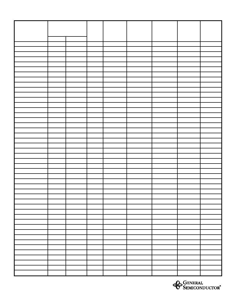
ELECTRICAL CHARACTERISTICS at (T
A
=
25∞C unless otherwise noted) TABLE 1 (Cont'd)
Maximum
Breakdown Voltage
Maximum
Peak Pulse
Maximum
Maximum
V
(BR)
Test
Stand-off
Reverse
Current
Clamping
Temperature
(Volts)
(NOTE 1)
Current
Voltage
Leakage
I
PPM
Voltage at
Coefficient
at I
T
V
WM
at V
WM
(NOTE 2)
I
PPM
of V
(BR)
Device Type
MIN
MAX
(mA)
(Volts)
I
D
(
µ
A)
(Amps)
V
C
(Volts)
(% / ∞C)
5KP33
36.7
44.9
5.0
33.0
10.0
84.7
59.0
0.104
5KP33A
36.7
40.6
5.0
33.0
10.0
93.8
53.3
0.104
5KP36
40.0
48.9
5.0
36.0
10.0
77.8
64.3
0.104
5KP36A
40.0
44.2
5.0
36.0
10.0
86.1
58.1
0.104
5KP40
44.4
54.3
5.0
40.0
10.0
70.0
71.4
0.105
5KP40A
44.4
49.1
5.0
40.0
10.0
77.5
64.5
0.105
5KP43
47.8
58.4
5.0
43.0
10.0
65.2
76.7
0.105
5KP43A
47.8
52.8
5.0
43.0
10.0
72.0
69.4
0.105
5KP45
50.0
61.1
5.0
45.0
10.0
62.3
80.3
0.106
5KP45A
50.0
55.3
5.0
45.0
10.0
68.8
72.7
0.106
5KP48
53.3
65.2
5.0
48.0
10.0
58.5
85.5
0.106
5KP48A
53.3
58.9
5.0
48.0
10.0
64.6
77.4
0.106
5KP51
56.1
69.3
5.0
51.0
10.0
54.9
91.1
0.107
5KP51A
56.7
62.7
5.0
51.0
10.0
60.7
82.4
0.107
5KP54
60.0
73.3
5.0
54.0
10.0
51.9
96.3
0.107
5KP54A
60.0
66.3
5.0
54.0
10.0
57.4
87.1
0.107
5KP58
64.4
78.7
5.0
58.0
10.0
48.5
103
0.107
5KP58A
64.4
71.2
5.0
58.0
10.0
53.4
94
0.107
5KP60
66.7
81.5
5.0
60.0
10.0
46.7
107
0.108
5KP60A
66.7
73.7
5.0
60.0
10.0
51.7
97
0.108
5KP64
71.1
96.9
5.0
64.0
10.0
43.9
114
0.108
5KP64A
71.1
78.6
5.0
64.0
10.0
48.5
103
0.108
5KP70
77.6
95.1
5.0
70.0
10.0
40.0
125
0.108
5KP70A
77.8
86.0
5.0
70.0
10.0
44.2
113
0.108
5KP75
83.3
102
5.0
75.0
10.0
37.3
134
0.108
5KP75A
83.3
92.1
5.0
75.0
10.0
41.3
121
0.108
5KP78
86.7
106.0
5.0
78.0
10.0
36.0
139
0.108
5KP78A
86.7
95.8
5.0
78.0
10.0
39.7
126
0.108
5KP85
94.4
115
5.0
85.0
10.0
33.1
151
0.108
5KP85A
94.4
104
5.0
85.0
10.0
36.5
137
0.110
5KP90
100
122
5.0
90.0
10.0
31.3
160
0.110
5KP90A
100
111
5.0
90.0
10.0
34.2
146
0.110
5KP100
111
136
5.0
100
10.0
27.9
179
0.110
5KP100A
111
123
5.0
100
10.0
30.9
162
0.110
5KP110
122
149
5.0
110
10.0
25.5
196
0.112
5KP110A
122
135
5.0
110
10.0
28.2
177
0.112
NOTES:
(1) V
(BR)
measured after I
T
applied for 300
µ
s I
T
=square wave pulse or equivalent
(2) Surge current waveform per Fig. 3 and derate per Fig. 2
(3) All items and symbols are consistent with ANSI/IEEE C62.35
APPLICATION
The 5KP series of high power transient voltage suppressors were designed to be used on the output of switching power supplies. These devices may be used to replace
crowbar circuits. Both the 5 and 10 percent voltage tolerances are referenced to the power supply output voltage level.
They are able to withstand high levels of peak current while allowing a circuit breaker to trip or a fuse blow before shorting. This will enable the user to reset the breaker or
replace the fuse and continue operation. For this type operation, it is recommended that a sufficient mounting surface be used for dissipating the heat generated by the
Transient Voltage Suppressor during the transient or over-voltage condition.
Transient Voltage Suppressors are Silicon PN Junction devices designed for absorption of high voltage transients associated with power disturbances, switching and
induced lighting effects. This series is available from 5.0 volts thru 110 volts.

0
1.0
2.0
3.0
4.0
0
100
150
50
0
50
100
150
200
0
25
50
75
100
25
75
125
175
0.1
µ
s
1.0
µ
s
10
µ
s
100
µ
s
1.0ms
10ms
0.1
1.0
10
100
1
10
100 200
100
1,000
10,000
100,000
1
10
100
100
200
300
400
350
250
150
0
25
50
75
100
125
150
175
200
0
6
8
4
2
RATINGS AND CHARACTERISTIC CURVES 5KP5.0 THRU 5KP110A
FIG. 1 - PEAK PULSE POWER RATING CURVE
P
PPM
, PEAK PULSE POWER, kW
td, PULSE WIDTH, sec.
T
A
, AMBIENT TEMPERATURE, ∞C
FIG. 4 - TYPICAL JUNCTION CAPACITANCE
FIG. 3 - PULSE WAVEFORM
t, TIME, ms
V
(BR)
, BREAKDOWN VOLTAGE, VOLTS
T
L,
LEAD TEMPERATURE,∞C
NUMBER OF CYCLES AT 60 H
Z
I
PPM,
PEAK PULSE CURRENT
, %
PEAK PULSE POWER (P
PP
) or CURRENT
(I
PP
)
DERA
TING IN PERCENT
AGE, %
C
J
, JUNCTION CAP
ACIT
ANCE, pF
I
FSM
, PEAK FOR
W
ARD SURGE CURRENT
,
AMPERES
NON-REPETITIVE
PULSE WAVEFORM
SHOWN in FIG. 3
T
A
= 25∞C
PULSE WIDTH (td) is DEFINED
as the POINT WHERE the PEAK
CURRENT DECAYS to 50% of I
PP
tr=10
µ
sec.
MEASURED at
ZERO BIAS
MEASURED at
STAND-OFF
VOLTAGE, V
WM
0.8 x 0.8 x 0.040" (20 x 20mm)
COPPER HEAT SINK
60 H
Z
RESISTIVE OR INDUCTIVE LOAD
8.3ms SINGLE HALF SINE-WAVE
(JEDEC Method)
td
HALF VALUE - I
PP
2
10/1000
µ
sec. WAVEFORM
as DEFINED BY R.E.A.
FIG. 6 - MAXIMUM NON-REPETITIVE FORWARD
SURGE CURRENT
PEAK VALUE
I
PPM
FIG. 5 - STEADY STATE POWER DERATING CURVE
PM
(A
V),
STEADY
ST
A
TE POWER DISSIP
A
TION,
W
A
TTS
FIG. 2 - PULSE DERATING CURVE
T
J
=25∞C
f=1 MHz
Vsig=50mVp-p
= 0.375" (9.5mm)
lead lengths
L