FEATURES
Small Signal Transistors (PNP)
Dimensions in inches and (millimeters)
.016 (0.4)
.056 (
1
.43
)
.037(0.95) .037(0.95)
ma
x
.
.004
(
0
.1
)
.122 (3.1)
.016 (0.4)
.016 (0.4)
3
1
2
Top View
.102 (2.6)
.007 (
0
.17
5
)
.0
45 (
1
.15)
.118 (3.0)
.052 (
1
.33
)
.005
(
0
.1
25)
.094 (2.4)
.0
37 (
0
.95)
Case: SOT-23 Plastic Package
Weight: approx. 0.008 g
MECHANICAL DATA
MAXIMUM RATINGS AND ELECTRICAL CHARACTERISTICS
Ratings at 25 ∞C
ambient temperature unless otherwise specified
Pin configuration
1 = Base, 2 = Emitter, 3 = Collector.
SOT-23
4/98
BC807, BC808
PNP Silicon Epitaxial Planar Transistors
for switching, AF driver and amplifier
applications.
Especially suited for automatic insertion
in thick- and thin-film circuits.
These transistors are subdivided into three groups -16,
-25 and -40 according to their current gain.
As complementary types, the NPN transistors BC817
and BC818 are recommended.
Symbol
Value
Unit
Collector-Emitter Voltage
BC807
BC808
≠V
CES
≠V
CES
50
30
V
V
Collector-Emitter Voltage
BC807
BC808
≠V
CEO
≠V
CEO
45
25
V
V
Emitter-Base Voltage
≠V
EBO
5
V
Collector Current
≠I
C
500
mA
Peak Collector Current
≠I
CM
1000
mA
Peak Base Current
≠I
BM
200
mA
Peak Emitter Current
I
EM
1000
mA
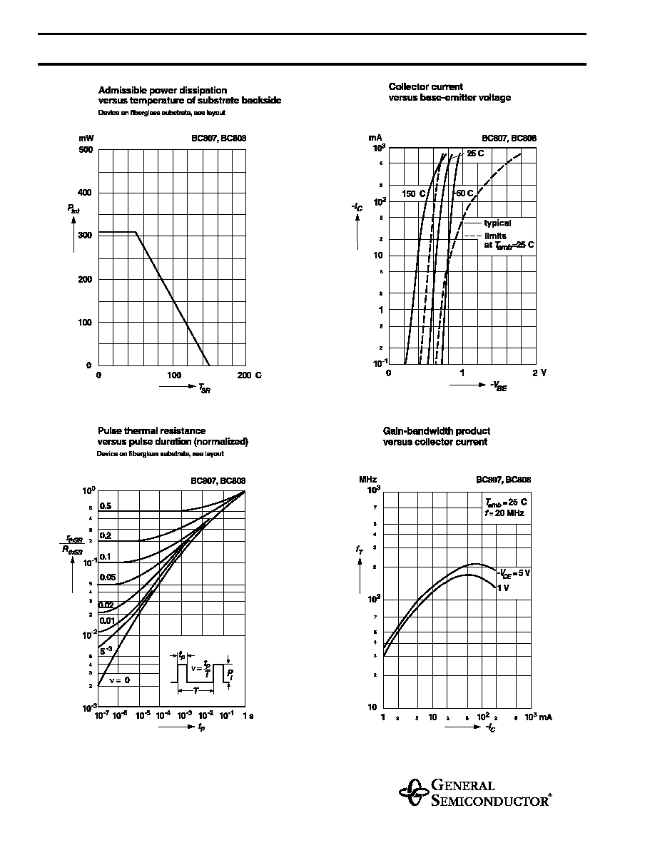
Power Dissipation at T
SB
= 50 ∞C
P
tot
310
1)
mW
Junction Temperature
T
j
150
∞C
Storage Temperature Range
T
S
≠ 65 to +150
∞C
1)
Device on fiberglass substrate, see layout
Marking code
Type
Marking
BC807-16
-25
-40
BC808-16
-25
-40
5A
5B
5C
5E
5F
5G

ELECTRICAL CHARACTERISTICS
Ratings at 25 ∞C
ambient temperature unless otherwise specified
BC807, BC808
Symbol
Min.
Typ.
Max.
Unit
DC Current Gain
at ≠V
CE
= 1 V, ≠I
C
= 100 mA
Current Gain Group-16
-25
-40
at ≠V
CE
= 1 V, ≠I
C
= 300 mA
-16
-25
-40
h
FE
h
FE
h
FE
h
FE
h
FE
h
FE
100
160
250
60
100
170
≠
≠
≠
≠
≠
≠
250
400
600
≠
≠
≠
≠
≠
≠
≠
≠
≠
Thermal Resistance Junction Substrate
Backside
R
thSB
≠
≠
320
1)
K/W
Thermal Resistance Junction to Ambient Air
R
thJA
≠
≠
450
1)
K/W
Collector Saturation Voltage
at ≠I
C
= 500 mA, ≠I
B
= 50 mA
≠V
CEsat
≠
≠
0.7
V
Base-Emitter Voltage
at ≠V
CE
= 1 V, ≠I
C
= 300 mA
≠V
BE
≠
≠
1.2
V
Collector-Emitter Cutoff Current
at ≠V
CE
= 45 V
BC807
at ≠V
CE
= 25 V
BC808
at ≠V
CE
= 25 V, T
j
= 150 ∞C
≠I
CES
≠I
CES
≠I
CES
≠
≠
≠
≠
≠
≠
100
100
5
nA
nA
µ
A
Emitter-Base Cutoff Current
at ≠V
EB
= 4 V
≠I
EBO
≠
≠
100
nA
Gain-Bandwidth Product
at ≠V
CE
= 5 V, ≠I
C
= 10 mA, f = 50 MHz
f
T
≠
100
≠
MHz
Collector-Base Capacitance
at ≠V
CB
= 10 V, f = 1 MHz
C
CBO
12
pF
1)
Device on fiberglass substrate, see layout
Layout for R
thJA
test
Thickness: Fiberglass 0.059 in (1.5 mm)
Copper leads 0.012 in (0.3 mm)
.59 (15)
0.2 (5)
.03 (0.8)
.30 (7.5)
.12 (3)
.04 (1)
.06 (1.5)
.20 (5.1)
.08 (2)
.08 (2)
.04 (1)
Dimensions in inches (millimeters)
.47 (12)