FEATURES
Small Signal Transistors (NPN)
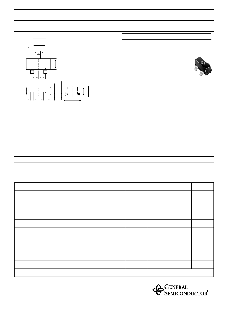
Dimensions in inches and (millimeters)
.016 (0.4)
.056 (
1
.43
)
.037(0.95) .037(0.95)
m
a
x
.
.0
04 (
0
.1)
.122 (3.1)
.016 (0.4)
.016 (0.4)
3
1
2
Top View
.102 (2.6)
.0
07 (
0
.175)
.045 (
1
.15)
.118 (3.0)
.052 (
1
.33
)
.
005 (
0
.125)
.094 (2.4)
.037 (
0
.95)
Case: SOT-23 Plastic Package
Weight: approx. 0.008 g
MECHANICAL DATA
MAXIMUM RATINGS AND ELECTRICAL CHARACTERISTICS
Ratings at 25 ∞C
ambient temperature unless otherwise specified
Pin configuration
1 = Base, 2 = Emitter, 3 = Collector.
SOT-23
4/98
NPN Silicon Epitaxial Planar Transistors
especially suited for application in class-B
video output stages of TV receivers and
monitors.
As complementary types, the PNP tran-
sistors BF821 and BF823 are recom-
mended.
BF820, BF822
Symbol
Value
Unit
Collector-Base Voltage
BF820
BF822
V
CBO
V
CBO
300
250
V
V
Collector-Emitter Voltage
BF822
V
CEO
250
V
Collector-Emitter Voltage
BF820
V
CER
300
V
Emitter-Base Voltage
V
EBO
5
V
Collector Current
I
C
50
mA
Peak Collector Current
I
CM
100
mA
Power Dissipation at T
SB
= 50 ∞C
P
tot
300
1)
mW
Junction Temperature
T
j
150
∞C
Storage Temperature Range
T
S
≠65 to +150
∞C
1)
Device on fiberglass substrate, see layout
Marking code
BF820 = 1V
BF822 = 1X
ELECTRICAL CHARACTERISTICS
Ratings at 25 ∞C
ambient temperature unless otherwise specified
BF820, BF822
Symbol
Min.
Typ.
Max.
Unit
Collector-Base Breakdown Voltage
BF820
at I
C
= 100
µ
A, I
B
= 0
BF822
V
(BR)CBO
V
(BR)CBO
300
250
≠
≠
≠
≠
V
V
Collector-Emitter Breakdown Voltage
BF822
at I
C
= 10
m
A, I
E
= 0
V
(BR)CEO
250
≠
≠
V
Collector-Emitter Breakdown Voltage
BF820
at R
BE
= 2.7 k
, I
C
= 10
m
A
V
(BR)CER
300
≠
≠
V
Emitter-Base Breakdown Voltage
at I
E
= 100
µ
A, I
B
= 0
V
(BR)EBO
5
≠
≠
V
Collector-Base Cutoff Current
at V
CB
= 200 V, I
E
= 0
I
CBO
≠
≠
10
nA
Collector-Emitter Cutoff Current
at R
BE
= 2.7 k
, V
CE
= 250 V
at R
BE
= 2.7 k
, V
CE
= 200 V, T
j
= 150 ∞C
I
CER
I
CER
50
10
nA
µ
A
Collector Saturation Voltage
at I
C
= 30 mA, I
B
= 5 mA
V
CEsat
≠
≠
0.6
V
DC Current Gain
at V
CE
= 20 V, I
C
= 25 mA
h
FE
50
≠
≠
≠
Gain-Bandwidth Product
at V
CE
= 10 V, I
C
= 10 mA
f
T
60
≠
≠
MHz
Feedback Capacitance
at V
CE
= 30 V, I
C
= 0, f = 1 MHz
C
re
≠
≠
1.6
pF
Thermal Resistance Junction to Ambient Air
R
thJA
≠
≠
430
1)
K/W
1)
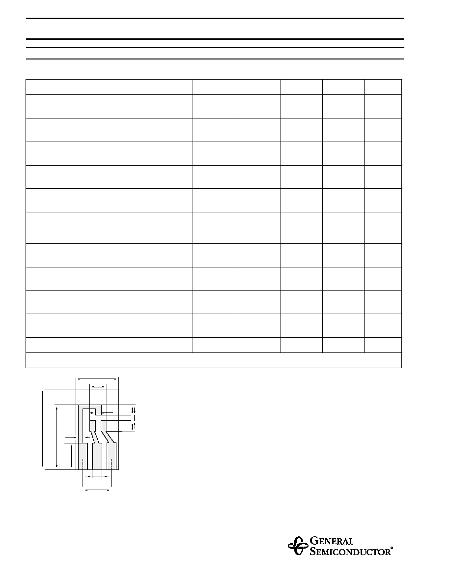
Device on fiberglass substrate, see layout
Layout for R
thJA
test
Thickness: Fiberglass 0.059 in (1.5 mm)
Copper leads 0.012 in (0.3 mm)
.59 (15)
0.2 (5)
.03 (0.8)
.30 (7.5)
.12 (3)
.04 (1)
.06 (1.5)
.20 (5.1)
.08 (2)
.08 (2)
.04 (1)
Dimensions in inches (millimeters)
.47 (12)