 | –≠–ª–µ–∫—Ç—Ä–æ–Ω–Ω—ã–π –∫–æ–º–ø–æ–Ω–µ–Ω—Ç: GFD50N03 | –°–∫–∞—á–∞—Ç—å:  PDF PDF  ZIP ZIP |
Maximum Ratings and Thermal Characteristics
(T
C
= 25∞C unless otherwise noted)
Parameter
Symbol
Limit
Unit
Drain-Source Voltage
V
DS
30
V
Gate-Source Voltage
V
GS
±
20
Continuous Drain Current
(1)
I
D
65
A
Pulsed Drain Current
I
DM
150
Maximum Power Dissipation
T
C
= 25∞C
P
D
62.5
W
T
C
= 100∞C
25.0
Operating Junction and Storage Temperature Range
T
J
, T
stg
≠55 to 150
∞C
Junction-to-Case Thermal Resistance
R
JC
2.0
∞C/W
Junction-to-Ambient Thermal Resistance
(2)
R
JA
40
∞C/W
Notes: (1) Maximum DC current limited by the package.
(2) 1-in
2
2oz. Cu PCB mounted
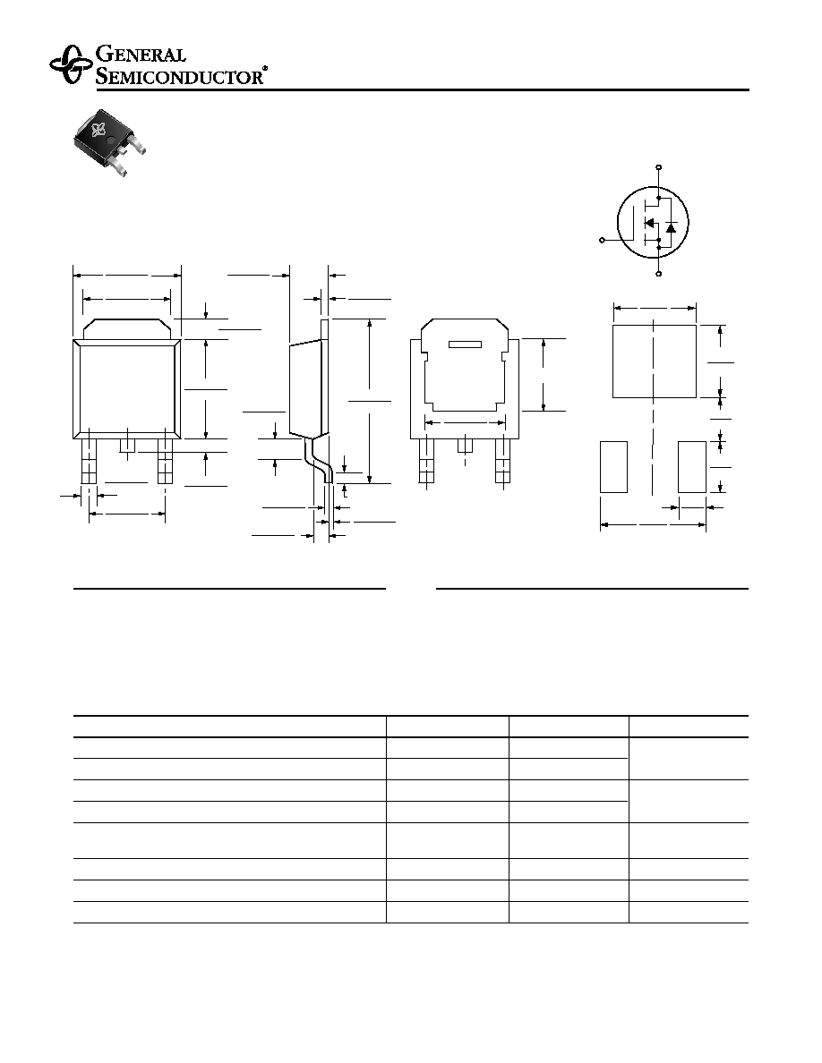
GFD50N03
N-Channel Enhancement-Mode MOSFET
V
DS
30V R
DS(ON)
9
m
I
D
65A
5/29/01
Features
∑ Advanced Trench Process Technology
∑ High Density Cell Design for Ultra Low On-Resistance
∑ Specially Designed for Low Voltage DC/DC Converters
and motor drives
∑ Fast Switching for High Efficiency
Mechanical Data
Case: JEDEC TO-252 molded plastic body
Terminals: Solder plated, solderable per
MIL-STD-750, Method 2026
High temperature soldering guaranteed:
250∞C/10 seconds at terminals
Weight: 0.011oz., 0.4g
0.190
(4.826)
0.243
(6.172)
0.063
(1.6)
0.165
(4.191)
0.100
(2.54)
0.118
(3.0)
0.245 (6.22)
0.235 (5.97)
0.040 (1.02)
0.025 (0.64)
0.410 (10.41)
0.380 (9.65)
0.170 (4.32) min.
0.214 (5.44)
0.206 (5.23)
0.265 (6.73)
0.255 (6.48)
0.023 (0.58)
0.018 (0.46)
0.094 (2.39)
0.087 (2.21)
0.204 (5.18)
0.156 (3.96)
0.197 (5.00)
0.177 (4.49)
0.035 (0.89)
0.028 (0.71)
G
S
D
0.023 (0.58)
0.018 (0.46)
0.045 (1.14)
0.035 (0.89)
0.009 (0.23)
0.001 (0.03)
0.020 (0.51)
min.
0.060 (1.52)
0.045 (1.14)
0.050 (1.27)
0.035 (0.89)
TO-252 (DPAK)
Dimensions in inches
and (millimeters)
Mounting Pad Layout
G
D
S
T
RENCH
G
EN
F
ET
Æ
New Product

Electrical Characteristics
(T
J
= 25∞C unless otherwise noted)
Parameter
Symbol
Test Condition
Min
Typ
Max
Unit
Static
Drain-Source Breakdown Voltage
BV
DSS
V
GS
= 0V, I
D
= 250
µ
A
30
--
--
V
Gate Threshold Voltage
V
GS(th)
V
DS
= V
GS
, I
D
= 250
µ
A
1.0
--
3.0
V
Gate-Body Leakage
I
GSS
V
DS
= 0V, V
GS
= ±20V
--
--
±100
nA
Zero Gate Voltage Drain Current
I
DSS
V
DS
= 30V, V
GS
= 0V
--
--
1.0
µ
A
On-State Drain Current
(1)
I
D(on)
V
DS
5V, V
GS
= 10V
50
--
--
A
Drain-Source On-State Resistance
(1)
R
DS(on)
V
GS
= 10V, I
D
= 15A
--
7.1
9
m
V
GS
= 4.5V, I
D
= 13A
--
10
12
Forward Transconductance
(1)
g
fs
V
DS
= 15V, I
D
= 15A
--
50
--
S
Dynamic
Total Gate Charge
Q
g
V
DS
=15V
,
V
GS
=5V, I
D
=15A
--
31
43
--
60
84
Gate-Source Charge
Q
gs
V
DS
= 15V, V
GS
= 10V
--
9
--
nC
Gate-Drain Charge
Q
gd
I
D
= 15A
--
8.5
--
Turn-On Delay Time
t
d(on)
--
13
26
Rise Time
t
r
V
DD
= 15V, R
L
= 15
--
16
29
Turn-Off Delay Time
t
d(off)
I
D
1A, V
GEN
= 10V
--
94
132
ns
Fall Time
t
f
R
G
= 6
--
38
57
Input Capacitance
C
iss
V
GS
= 0V
--
3240
--
Output Capacitance
C
oss
V
DS
= 15V
--
625
--
pF
Reverse Transfer Capacitance
C
rss
f = 1.0MH
Z
--
285
--
Source-Drain Diode
Max Diode Forward Current
I
S
--
--
--
20
A
Diode Forward Voltage
(1)
V
SD
I
S
= 20A, V
GS
= 0V
--
0.85
1.3
V
Note: (1) Pulse test; pulse width
300
µ
s, duty cycle
2%
GFD50N03
N-Channel Enhancement-Mode MOSFET
G
D
S
V
IN
V
DD
V
GEN
R
G
R
D
V
OUT
DUT
Input, V
IN
t
d(on)
Output, V
OUT
t
on
t
r
t
d(off)
t
off
t
f
INVERTED
90%
10%
10%
90 %
50%
50%
10%
90%
PULSE WIDTH
Switching
Test Circuit
Switching
Waveforms
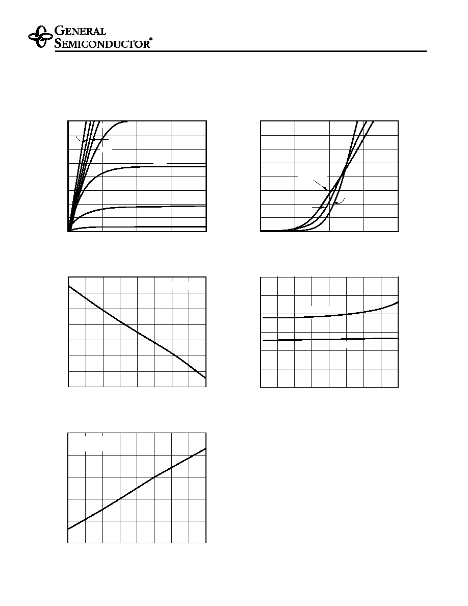
0
10
20
30
50
60
70
0
1
2
3
4
Fig. 1 ≠ Output Characteristics
0
0.0025
0.005
0.0075
0.01
0.0125
0.015
0
20
40
50
60
80
Fig. 4 ≠ On-Resistance vs.
Drain Current
0
10
20
40
30
50
80
60
1
2
3
4
5
Fig. 2 ≠ Transfer Characteristics
40
V
GS
= 2.5V
0.8
0.6
1.4
1.6
1.2
1
--50
--25
25
50
75
100
125
150
0
Fig. 5 ≠ On-Resistance vs.
Junction Temperature
V
GS
= 10V
I
D
= 15A
V
GS
= 4.5V
25
∞
C
V
GS
= 10V
T
J
= 125
∞
C
--55
∞
C
3.0V
3.5V
6.0V
4.0V
V
DS
= 10V
10V
0.6
1.4
1.2
1.6
1.8
0.8
1
--50
--25
25
50
75
100
125
150
0
Fig. 3 ≠ Threshold Voltage
I
D
= 250
µ
A
I
D
-
-
Drain-to-Source Current (A)
V
DS
-- Drain-to-Source Voltage (V)
R
DS(ON)
-
-
On-Resistance (
)
I
D
-- Drain Current (A)
I
D
-
-
Drain Current (A)
V
GS
-- Gate-to-Source Voltage (V)
R
DS(ON)
-
-
On-Resistance
(Normalized)
T
J
-- Junction Temperature (
∞
C)
V
(th)
-
-
Gate-to-Source
Threshold
V
oltage (V)
T
J
-- Junction Temperature (
∞
C)
80
5.0V
2
10
70
30
70
4.5V
Ratings and
Characteristic Curves
(T
A
= 25∞C unless otherwise noted)
GFD50N03
N-Channel Enhancement-Mode MOSFET
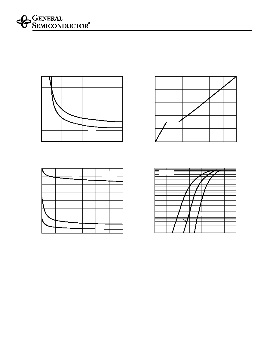
0
500
1000
1500
2000
2500
3000
3500
4000
0
5
10
15
30
20
25
Fig. 8 ≠ Capacitance
C
iss
C
rss
C
oss
f = 1MH
Z
V
GS
= 0V
0
2
4
6
8
10
0
10
20
40
30
Fig. 7 ≠ Gate Charge
50
60
V
DS
= 15V
I
D
= 15A
0.01
0.1
1
10
100
0
0.2
0.4
0.6
0.8
1
1.2
1.4
T
J
= 125
∞
C
Fig. 9 ≠ Source-Drain Diode
Forward Voltage
25
∞
C
--55
∞
C
V
GS
= 0V
I
S
-
-
Source Current (A)
V
SD
-- Source-to-Drain Voltage (V)
Q
g
-- Gate Charge (nC)
V
GS
-
-
Gate-to-Source V
oltage (V)
C -
-
Capacitance (pF)
V
DS
-- Drain-to-Source Voltage (V)
0
0.005
0.01
0.02
0.015
0.025
0.03
2
4
6
8
10
Fig. 6 ≠ On-Resistance vs.
Gate-to-Source Voltage
I
D
= 15A
T
J
= 125
∞
C
25
∞
C
R
DS(ON)
-
-
On-Resistance (
)
V
GS
-- Gate-to-Source Voltage (V)
Ratings and
Characteristic Curves
(T
A
= 25∞C unless otherwise noted)
GFD50N03
N-Channel Enhancement-Mode MOSFET
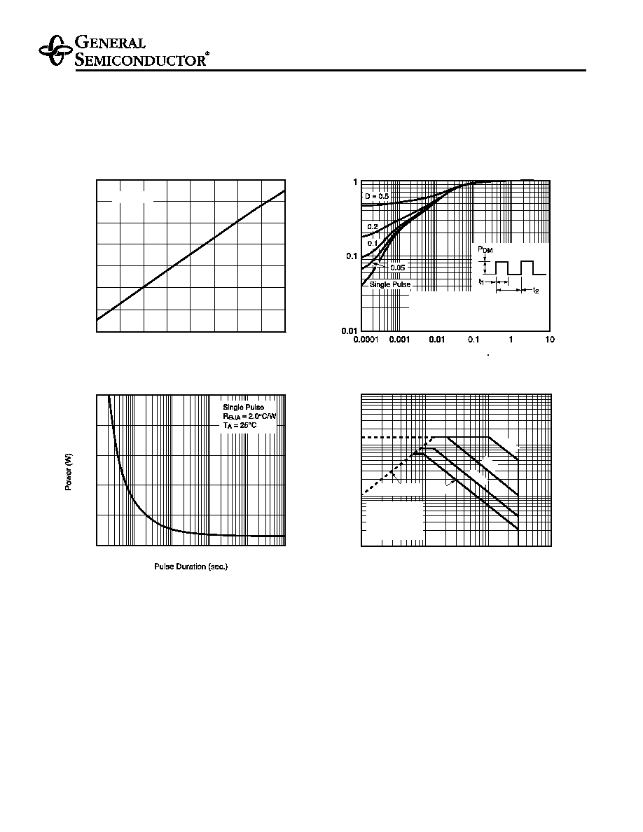
Ratings and
Characteristic Curves
(T
A
= 25∞C unless otherwise noted)
GFD50N03
N-Channel Enhancement-Mode MOSFET
Fig. 11 ≠ Transient Thermal
Impedance
Fig. 12 ≠ Power vs. Pulse Duration
0.1
0.01
0.001
0.0001
0
200
400
600
800
1000
1
10
37
36
38
40
43
39
--50
--25
25
50
75
100
125
0
Fig. 10 ≠ Breakdown Voltage
vs. Junction Temperature
150
I
D
= 250
µ
A
BV
DSS
-
-
Breakdown V
oltage (V)
R
JA
(norm)
-
-
Normalized
Thermal
Impedance
T
J
-- Junction Temperature (
∞
C)
Pulse Duration (sec.)
41
42
1. Duty Cycle, D = t
1
/ t
2
2. R
JA
(t) = R
JA
(norm) *R
JA
3. R
JA
= 2.0
∞
C/W
4. T
J
-- T
A
= P
DM
* R
JA
(t)
Fig. 13 ≠ Maximum Safe Operating Area
V
DS
-- Drain-Source Voltage (V)
0.1
1
1
10
100
1000
10
100
V
GS
= 10V
Single Pulse
R
JC
= 2.0
∞
C/W
T
A
= 25
∞
C
I
D
-
-
Drain Current (A)
1ms
100
µ
s
10ms
DC
R
DS(ON)
Limit