
DATA SHEET
DEVICE DESCRIPTION
The GF9102A is a linear phase FIR digital filter that is usable
in a variety of video signal processing applications. The device
contains three separate fixed coefficient filters and can be
operated in three basic modes: 53 tap low pass filter, 9 tap
chroma bandpass filter or 21 tap chroma bandpass filter.
In the 53 tap low pass filter mode, the GF9102A can replace the
TMC2242 in all applications, except those requiring 1:1 low
pass filtering, for improved performance and full CCIR 601
compatibility. Specific improvements include true unity gain at
DC, 12.4 dB attenuation at s/4 with a single device, reduced
output ringing with constant input in interpolate mode, support
for signed and unsigned data formats, rounding to 10 and 8 bit
CCIR 601 data formats, masking of serial digital TRS codes in
the data stream, and elimination of the non-saturated-type
overflow condition. The device can be operated in both
TMC2242 compatible modes and in GF9102A enhanced
modes.
When used as a decimating post-filter with a double speed
oversampling analog-digital converter, the device greatly
reduces the cost and complexity of the associated analog
anti-aliasing pre-filter. In a similar fashion, when used as an
interpolating pre-filter with a double speed oversampling digital-
analog converter, the GF9102A simplifies the analog
reconstruction post-filter. The GF9102A also exceeds the
requirements for conversion between 4:2:2 and 4:4:4 signal
formats.
For chroma filtering applications, the GF9102A can be operated
as a 9 or 21 tap bandpass filter by selecting the appropriate
operating mode.
The GF9102A is packaged in a 44 pin PLCC and is pin
compatible with the TMC2242. The device operates with a
single +5 V supply.
FEATURES
∑ improved performance over TMC2242 in applications
not requiring 1:1 low pass filtering
∑ low power (60mA typical at = 20MHz)
∑ 40 MHz maximum clock rate
∑ single device exceeds CCIR 601 lowpass filter
requirements
∑ true unity gain (0.0 dB) at DC
∑ reduced output ringing with constant input in
interpolation mode
∑ built-in TRS code protection
∑ 12 bit inputs and 16 bit outputs in 2's complement
signed or unsigned formats
∑ user-selectable 8 to 16 bit output rounding
∑ can also be operated as a 9 or 21 tap chroma
bandpass filter under user control
∑ single +5 V power supply
∑ three state outputs
APPLICATIONS
∑ CCIR 601-compliant oversampling video A/D and
D/A conversion
∑ 2:1 interpolation and decimation
∑ 4:2:2 to 4:4:4 format conversion
∑ Chroma bandpass filtering
Multi
G E N
G E N
TM
GF9102A
Decimating/Interpolating Digital Filter
INPUT
PROCESSING
UNIT
OUTPUT FORMAT
TIMING CONTROLS
CLK
DEC
SYNC
DATA IN
SI11..0
BPF1
OUTPUT
PROCESSING
UNIT
INT
TCO
BPF2
53 TAP LPF
M
U
X
SO3..0
RND2..0
DATA OUT
SO15..0
OE
FUNCTIONAL BLOCK DIAGRAM
Revision Date: February 1996
ORDERING INFORMATION
Part Number Package Type Temperature Range
GF9102ACPM 44 Pin PLCC 0
∞
to 70
∞
C
GF9102ACTM 44 Pin PLCC Tape 0
∞
to 70
∞
C
GENNUM CORPORATION P.O. Box 489, Stn A, Burlington, Ontario, Canada L7R 3Y3 tel. (905) 632-2996 fax: (905) 632-5946
Gennum Japan Corporation: A-302 Miyamae Village, 2-10-42 Miyamae, Suginami-ku, Tokyo 168, Japan tel. (03) 3334-7700 fax (03) 3247-8839
Document No. 521 - 26 - 02

2
521 - 26 - 02
CLK
42
I
System Clock.
TTL input. All timing specifications are referenced to the rising edge of clock.
SYNC
43
I
Data Synchronization.
TTL input with internal pull-up. This input is used to synchronize the
incoming data with the GF9102A by holding SYNC high on clock N and low on clock N+1 when
the first data word is presented to the input SI
11..0
. SYNC may be held low until
resynchronization is desired, or it may be clocked at half the clock rate.
SI
11..0
40, 37, 36, 35,
I
Input Data Port.
TTL inputs with internal pull-downs. Data is presented to this registered 12-bit
34, 33, 32, 31,
data input port. This port can be programmed as two's complement signed or unsigned binary
30, 27, 26, 25
format. See the following section on input data format. Data is latched internally on every clock in
decimate mode, and on every other clock in interpolate mode. SI
11
is the MSB.
Two's Complement Output Format Control.
TTL input with internal pull-down. When TCO is high,
output data is presented in two's complement format. When TCO is low, the output is inverted
offset binary, obtained by inverting bits SO
14
through SO
0
, leaving SO
15
unchanged.
Interpolate.
Active low TTL input with internal pull-up. When the interpolate control is low, data
is input at full clock speed and the chip inserts zeros between samples, padding the input to
match the output rate. The GF9102A then interpolates between these alternate input data points to
achieve full output data rate.
DEC
1
I
Decimate.
Active low TTL input with internal pull-down. When the decimate control is low, the
output register is driven at half system clock speed, decimating the output data stream. When
DEC and INT are low, the GF9102A will be programmed as a 21 tap or 9 tap bandpass filter
depending on the state of the SYNC input. See Operation Mode Control below for more detail.
Output Rounding Control.
TTL inputs with internal pull-down. These pins set the position of the
effective least significant bit of the output port by adding a rounding bit to the next lower internal bit
and zeroing all outputs below the rounding bit. Additional rounding functions are added with the
SO
1
control input. See Table 6.
Output Data Port.
TTL outputs (SO
3..0
are bi-directional pins with an internal pull-down). The
filtered result is available at this registered 16-bit output port, half LSB rounded as determined by
the rounding control word RND
2..0
. SO
15
is the MSB. The SO
3..0
control inputs enable additional
formatting and rounding features as described below.
Output Data Port.
TTL bi-directional pins with internal pull-down. The SO
0
control input enables
the unsigned input and output format. The SO
1
control input enables 8-bit rounding or CCIR 601
8-bit and 10-bit modes of operation. SO
3..2
are reserved for future functions.
Output Enable.
Active low TTL input with internal pull-up. When this asynchronous input is high,
the output data port is in the high impedance state.
+5 V
±
5% power supply.
Ground
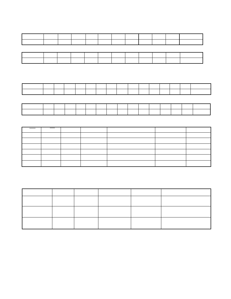
PIN DESCRIPTION
SYMBOL
PIN NO.
TYPE
DESCRIPTION
TCO
2
I
INT
44
I
RND
2..0
22, 23, 24
I
SO
15..0
4, 5, 6, 7,
O
8, 9, 10, 11,
14, 15, 16, 17,
18, 19, 20, 21
SO
3..0
18, 19, 20, 21
I/O
OE
3
I
VDD
13, 29, 38
GND
12, 28, 39, 41

3
521 - 26 - 02
SI
2
SI
1
SI
0
RND
0
RND
1
RND
2
SO
0
SO
1
SO
2
SO
3
GND
V
DD
SI
10
SI
9
SI
11
GND
CLK
SYNC
TCO
SO
15
SO
14
SO
13
GF9102A
TOP VIEW
7
8
9
10
11
12
13
14
15
16
17
18 19 20 21 22 23 24 25 26 27 28
6 5 4 3 2 1 44 43 42 41 40
GND
SI
8
SI
7
SI
6
SI
5
SI
4
SI
3
SO
12
SO
11
SO
10
SO
9
SO
8
GND
V
DD
SO
7
SO
4
SO
5
SO
6
V
DD
39
38
37
36
35
34
33
32
31
30
29
INT
DEC
OE
PARAMETER VALUE
Filter Order
53
Pass Band Ripple
<
±
0.02 dB
Pass Band Edge
5.75 MHz
DC Gain
0.00 dB
6.75 MHz (s/4) Attenuation
12.4 dB
Minimum Stop Band Attenuation
>58 dB
Stop Band Edge
7.4 MHz
LOWPASS FILTER CHARACTERISTICS at SAMPLING FREQUENCY OF 27MHz
Fig. 1 GF9102A Pin Connections

4
521 - 26 - 02
frequency (MHz)
0
21 TAP BPF
9 TAP BPF
dB
-80
-70
-60
-50
-40
-30
-20
-10
0
0
2
4
6
8
10
12
14
CCIR601
GF9102
freq enc
(MH )
0
21 TAP BPF
9 TAP BPF
21 TAP BPF
9 TAP BPF
Fig. 6 Frequency Response of the Bandpass
Filter Transition Band (Sampling at 14.31818 MHz)
0 10 20 30 40 50 60 70 80
SAMPLE NUMBER
Fig. 4 Step Response of Decimation Filter
0 1 2 3 4 5 6 7
FREQUENCY (MHz)
Fig. 5 Frequency Response of the Bandpass
Filter (Sampling at 14.31818 MHz)
1.5 2 2.5 3 3.5 4 4.5 5 5.5
FREQUENCY (MHz)
21 TAP BPF
9 TAP BPF
21 TAP BPF
9 TAP BPF
Fig. 3 Frequency Response of the Decimation/Interpolation
Filter Passband (Sampling at 27 MHz)
% FULL SCALE
MAGNITUDE (dB) 21 TAP BPF
MAGNITUDE (dB) 21 TAP BPF
6
5
4
3
2
1
0
-1
-2
-3
-4
MAGNITUDE (dB) 9 TAP BPF
6
-15
-36
-58
-79
-100
MAGNITUDE (dB) 9 TAP BPF
Fig. 7 Frequency Response of the Bandpass Filter
Passband (Sampling at 14.31818 MHz)
MAGNITUDE (dB) 21 TAP BPF
21 TAP BPF
9 TAP BPF
MAGNITUDE (dB) 9 TAP BPF
6.02
6.015
6.01
6.005
6.00
Fig. 2 Frequency Response of the Decimation/Interpolation
Filter (Sampling at 27 MHz)
MAGNITUDE (dB)
0
-10
-20
-30
-40
-50
-60
-70
-80
0 2 4 6 8 10 12 14
FREQUENCY (MHz)
CCIR601
GF9102A
0
0
1
2
3
4
5
6
CCIR601
CCIR601
GF9102
CCIR601
GF9102A
0 1 2 3 4 5 6
FREQUENCY (MHz)
0.05
0.0375
0.025
0.0125
0
-0.0125
-0.025
-0.0375
-0.05
MAGNITUDE (dB)
2.579545 3.079545 3.579545 4.079545 4.579545
FREQUENCY (MHz)
110
100
90
80
70
60
50
40
30
20
10
0
-10
0
-20
-40
-60
-80
-100
0
-0.005
-0.01
-0.015
-0.02
0
-1
-2
-3
-4
-5
-6
-7
-8
-9
-10
5
521 - 26 - 02
Table 1: Input Data Format and Bit Weighting
Two's complement signed binary, data range: -1
SI < 1
SI
11
SI
10
SI
9
SI
8
SI
7
SI
6
SI
5
SI
4
SI
3
SI
2
SI
1
SI
0
-2
0
2
-1
2
-2
2
-3
2
-4
2
-5
2
-6
2
-7
2
-8
2
-9
2
-10
2
-11
Unsigned binary, data range: 0
SI < 256
SI
11
SI
10
SI
9
SI
8
SI
7
SI
6
SI
5
SI
4
SI
3
SI
2
SI
1
SI
0
2
7
2
6
2
5
2
4
2
3
2
2
2
1
2
0
2
-1
2
-2
2
-3
2
-4
Table 2: Output Data Format and Bit Weighting
Two's complement signed binary, data range: -1
SO < 1
SO
15
SO
14
SO
13
SO
12
SO
11
SO
10
SO
9
SO
8
SO
7
SO
6
SO
5
SO
4
SO
3
SO
2
SO
1
SO
0
-2
0
2
-1
2
-2
2
-3
2
-4
2
-5
2
-6
2
-7
2
-8
2
-9
2
-10
2
-11
2
-12
2
-13
2
-14
2
-15
Unsigned binary, data range: 0
SO < 256
SO
15
SO
14
SO
13
SO
12
SO
11
SO
10
SO
9
SO
8
SO
7
SO
6
SO
5
SO
4
SO
3
SO
2
SO
1
SO
0
2
7
2
6
2
5
2
4
2
3
2
2
2
1
2
0
2
-1
2
-2
2
-3
2
-4
2
-5
2
-6
2
-7
2
-8
Table 3: Operation Mode Control
DEC INT Sync Mode Description Device Latency Notes
0
0
0
Bandpass1
21 Tap Bandpass
18 Clock Cycles
2
0
0
1
Bandpass2
9 Tap Bandpass Gain=2
18 Clock Cycles
2
0
1
Sync
Decimating
Gain=1
33 Clock Cycles
1
1
0
Sync
Interpolating
Gain=0.5
33 Clock Cycles
1
1
0
Sync
Interpolating
Gain=1 for unsigned input
3
33 Clock Cycles
2
1
1
Sync
Pass through
Top 12 bit pass through
33 Clock Cycles
2
Notes:
1. This operating mode is compatible with TMC2242.
2. This is an enhanced operating mode of the GF9102A.
3. This mode is invoked using the SO
0
pin. See I/O Format control below.
Table 4: I/O Format Control
RND
2..0
SO
0
3
TCO
Input
5
Output
5
Notes
RND = 000
Output
0
Signed
I_Unsigned
1
1
Signed
Signed
RND
000
0
0
Signed
I_Unsigned
1
1
Signed
Signed
RND
000
1
0
Unsigned
4
Unsigned
2
1
Unsigned
Signed Limit output up to 15 bits
Notes:
1.
This operating mode is compatible with TMC2242.
2.
This is an enhanced operating mode of the GF9102A.
3.
SO
0
, the LSB of the output is a bi-directional pad with a large pull-down resistor. This pin does not have to be connected.
When this pin is not connected the GF9102A defaults to a mode compatible with the TMC2242.
4.
Application notes for the TMC2242 suggest grounding the MSB of the input if the input data is unsigned as
in most A/D converters. This method limits the input to 11 bits and leads to potential output non-saturated type overflow
since the MSB of the output is ignored.
5.
Signed: two's complement binary data.
I_unsigned: invert all bits in signed data except for the MSB; also called inverted offset binary.
Unsigned: invert MSB of signed data; also called offset binary.