www.gennum.com
GS9078A HD-LINXÆ II
Multi-Rate Cable Driver
GS9078A Data Sheet
34165 - 4
March 2006
1 of 14
Features
∑
SMPTE 259M and SMPTE 344M compliant
∑
Dual coaxial cable driving outputs with selectable
slew rate
∑
50
differential PECL input
∑
Pb-free and RoHS compliant
∑
Seamless interface to other HD-LINXÆ II family
products
∑
Single 3.3V power supply operation
∑
Operating temperature range: 0∞C to 70∞C
Applications
∑
SMPTE 259M and SMPTE 344M Coaxial Cable
Serial Digital Interfaces.
Description
The GS9078A is a second generation high-speed
BiCMOS integrated circuit designed to drive one or two
75
co-axial cables.
The GS9078A may drive data rates up to 540Mb/s and
provides two selectable slew rates in order to achieve
compliance to SMPTE 259M and SMPTE 344M.
The GS9078A accepts a LVPECL level differential input
that may be AC coupled. External biasing resistors at
the inputs are not required.
Power consumption is typically 168mW using a 3.3V
power supply. The GS9078A is Pb-free, and the
encapsulation compound does not contain halogenated
flame retardant.
This component and all homogeneous subcomponents
are RoHS compliant.
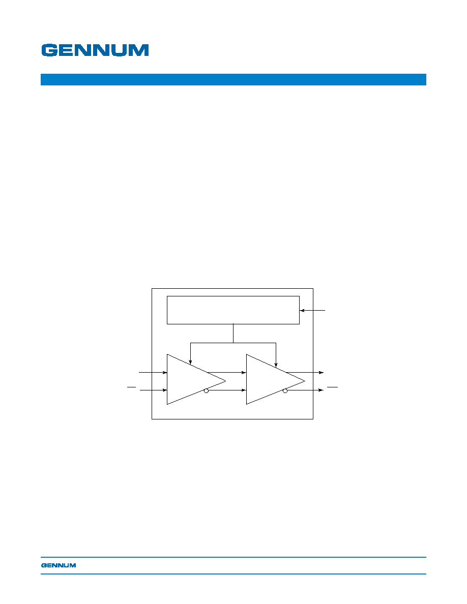
Functional Block Diagram
SDO
R
SET
SDO
SDI
SDI
BANDGAP REFERENCE AND BIASING CIRCUIT
OUTPUT STAGE &
CONTROL
INPUT
DIFFERENTIAL
PAIR

GS9078A Data Sheet
34165 - 4
March 2006
2 of 14
Contents
1. Pin Out ......................................................................................................................3
1.1 Pin Assignment ...............................................................................................3
1.2 Pin Descriptions ..............................................................................................3
2. Electrical Characteristics...........................................................................................4
2.1 Absolute Maximum Ratings ............................................................................4
2.2 Solder Reflow Profiles .....................................................................................4
2.3 DC Electrical Characteristics ..........................................................................5
2.4 AC Electrical Characteristics ...........................................................................6
3. Input / Output Circuits ...............................................................................................7
4. Detailed Description ..................................................................................................8
4.1 Input Interfacing ..............................................................................................8
4.2 Output Interfacing ...........................................................................................8
4.3 Output Return Loss Measurement ................................................................10
4.4 Output Amplitude (RSET) .............................................................................10
5. Application Information............................................................................................11
5.1 PCB Layout ...................................................................................................11
5.2 Typical Application Circuit .............................................................................11
6. Package & Ordering Information.............................................................................12
6.1 Package Dimensions ....................................................................................12
6.2 Recommended PCB Footprint ......................................................................13
6.3 Packaging Data .............................................................................................13
6.4 Ordering Information .....................................................................................13
7. Revision History ......................................................................................................14

GS9078A Data Sheet
34165 - 4
March 2006
3 of 14
1. Pin Out
1.1 Pin Assignment
Figure 1-1: 16-Pin QFN
1.2 Pin Descriptions
GS9078A
(top view)
1
V
EE
SDI
SDI
2
3
4
SDO
SDO
VCC
12
11
10
9
5
7
6
8
NC
NC
NC
NC
13
14
15
16
Center Pad
(bottom of package)
NC
NC
NC
NC
RSET
NC
Table 1-1: Pin Descriptions
Pin Number
Name
Timing
Type
Description
1,2
SDI, SDI
Analog
Input
Serial digital differential input.
3
V
EE
≠
Power
Most negative power supply connection. Connect to GND.
4
R
SET
Analog
Input
External output amplitude control resistor.
5,6,7,8,10,
13,14,15,16
NC
≠
≠
No Connect. Not bonded internally.
9
V
CC
≠
Power
Most positive power supply connection. Connect to +3.3V.
11,12
SDO, SDO
Analog
Output
Serial digital differential output.
≠
Center Pad
≠
Power
Connect to most negative power supply plane following the
recommendations in
Recommended PCB Footprint on
page 13
.

GS9078A Data Sheet
34165 - 4
March 2006
4 of 14
2. Electrical Characteristics
2.1 Absolute Maximum Ratings
2.2 Solder Reflow Profiles
The device is manufactured with Matte-Sn terminations and is compatible with both
standard eutectic and Pb-free solder reflow profiles. MSL qualification was
performed using the maximum Pb-free reflow profile shown in
Figure 2-1
.The
recommended standard Pb reflow profile is shown in
Figure 2-2
.
Figure 2-1: Maximum Pb-free Solder Reflow Profile (Preferred)
Parameter
Value
Supply Voltage
-0.5V to 3.6 V
DC
Input ESD Voltage
2kV
Storage Temperature Range
-50∞C < T
s
< 125∞C
Input Voltage Range (any input)
-0.3 to (V
CC
+0.3)V
Operating Temperature Range
0∞C to 70∞C
Reflow Temperature
260∞C
25∞C
150∞C
200∞C
217∞C
260∞C
250∞C
Time
Temperature
8 min. max
60-180 sec. max
60-150 sec.
20-40 sec.
3∞C/sec max
6∞C/sec max

GS9078A Data Sheet
34165 - 4
March 2006
5 of 14
Figure 2-2: Standard Pb Reflow Profile (Pb-free package)
2.3 DC Electrical Characteristics
25∞C
100∞C
150∞C
183∞C
230∞C
220∞C
Time
Temperature
6 min. max
120 sec. max
60-150 sec.
10-20 sec.
3∞C/sec max
6∞C/sec max
Table 2-1: DC Electrical Characteristics
V
DD
= 3.3V, T
A
= 0∞C to 70∞C, unless otherwise shown
Parameter
Symbol
Conditions
Min
Typ
Max
Units
Supply Voltage
V
CC
≠
3.135
3.3
3.465
V
Power Consumption
P
D
T
A
= 25∞C
≠
168
≠
mW
Supply Current
I
s
T
A
= 25∞C
≠
51
64
mA
Output Voltage
V
CMOUT
Common mode
≠
V
CC
- V
OUT
≠
V
Input Voltage
V
CMIN
Common mode
1.6 +
V
SDI
/2
≠
V
CC
-
V
SDI
/2
V