7
2
3
6
1
10
9
5
8
LOGIC
INPUT
INTERFACE
GND
MODE
CONTROL
CT
N/C
4
CONTROL
LOGIC
DIGITAL
TO
ANALOG
LINEAR
TO LOG
CONVERTER
CURRENT
CONTROLLED
RESISTANCE
CLOCK
OSCILLATOR
UP
CONTROL
DOWN
CONTROL
RA
RB
LOGIC SUPPLY
(MEMORY)
ANALOG
SUPPLY
FEATURES
∑
1.0 to 5 V DC supply voltage
∑
70
µ
A of analog current drain (typical)
∑
6
µ
A of memory current drain (typical)
∑
single or dual switch control
∑
touch plate compatible, (30 M
typ. impedance)
∑
typical 42 dB range
∑
adjustable clock frequency increases or decreases
time required to change diode impedance
Digitally Controlled
Transconductance Block
GT560 DATA SHEET
STANDARD PACKAGING
∑ 10 pin PLID
Æ
∑ Chip (79 x 60 mils)
Document No. 510 - 64 - 03
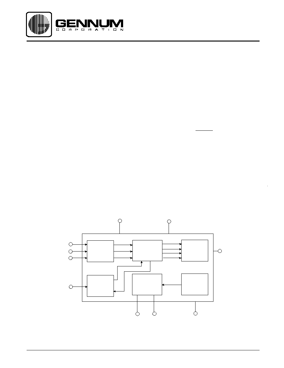
CIRCUIT DESCRIPTION
The GT560 is a low voltage transconductance block which
can be used as an electronic volume control. The
transconductance element consists of two diodes back-to-
back, whose impedance is varied by changing the amount of
current through the diodes.
The impedance of the diodes is controlled by digital circuitry
which consists of:
∑ an oscillator with an external capacitor,
C
T
, to set the
ramp frequency
c,
5 x 10
-7
c
C
T
∑ logic interface, which senses the volume up-down controls
∑ a digital / analog converter
∑ the control logic/debounce logic
∑ synchronous up-down counter
To increase or decrease the GT560 impedance, the switching
mechanism can be touch sensitive contacts or a mechanical
switch. In either configuration, the switches are connected
from pin 8 to V
CC
and pin 9 to V
CC
. Any resistance (30 M
typ.),
from pin 8 or 9 to V
CC
will activate the GT560 control circuitry
and the device will change impedance levels.
BLOCK DIAGRAM
Revision Date: January 2001
GENNUM CORPORATION P.O. Box 489, Stn. A, Burlington, Ontario, Canada L7R 3Y3 tel. +1 (905) 632-2996
Web Site: www.gennum.com E-mail: hipinfo@gennum.com

2
510 - 64 - 03
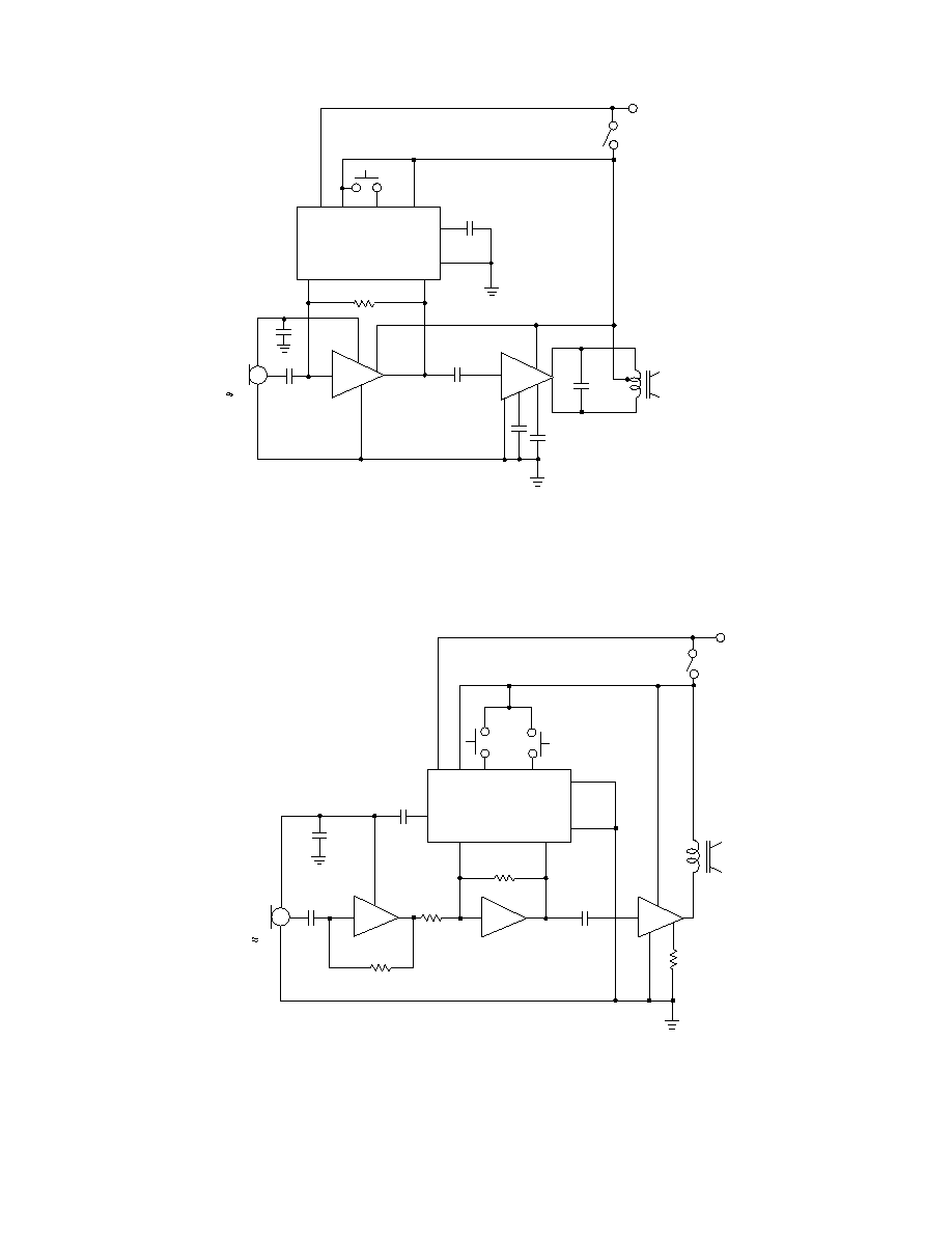
OPERATION
The impedance can be controlled using one of two methods.
The first method utilizes a Single Pole Single Throw (SPST),
momentary contact switch which combines the up/down
function in one action (see Fig. 2). The second method (see
Fig. 3) uses one Single Pole Double Throw (SPDT), or two SPST
switches which provide a separate action for the up-down
function. These switches can be mechanical or touch sensitive.
To operate the GT560 using a single switch, the Mode Control
(MC) is connected to the positive supply, the switch will then act
in an alternating manner first increasing impedance when
activated, then decreasing impedance when activated a second
time, both at a rate determined by the external timing capacitor.
If separate UP or DOWN switches are used, the Mode Control
pin connects to ground. Making contact to the DOWN switch,
the diode impedance will decrease until the switch is released
or the diodes reach minimum impedance (4 k
). Similarly,
contact to the UP switch will increase the diodes impedance
until the switch is released or the maximum value of diode
impedance has been reached (500 k
).
Once the minimum (4 k
) or maximum (500 k
) impedance is
reached and the switch is still closed, the impedance will stop
changing until the switch is released and the direction is
reversed. Should both switches be closed simultaneously, the
output impedance will remain unchanged.
In order for the GT560 to be activated and change impedance
the switch must be pressed for at least one time constant,
t
C
,
where t
C
=
1
C
Normally the timing capacitor
C
T
, is connected to ground, as
shown in Figure 1. When the circuit is turned on,
C
T
is required
to charge from 0 V
DC
to approximately 0.56 V
DC
. During this
charge up condition, the clock is disabled and ramping of the
impedance by the touch contacts or switches will be inactive
until
C
T
is charged.
Small values of
C
T
eg. 0.1
µ
F, will cause a time delay of
less than 2 seconds, however as the value of
C
T
is increased,
eg. 1.0
µ
F the charge time can be as high as 20 seconds.
If the length of the charge time is undesirable, the capacitor
can be referenced to a microphone decoupling point as shown
in Figure 3. In this configuration the capacitor charge time will
be less than 2 seconds with a 1.0
µ
F capacitor.
It is required that
C
T
be connected to a positive reference
voltage which has a high supply line rejection ratio, such as a
voltage regulator, or a microphone decoupling point. If
C
T
was
referenced directly to the supply, any battery line signals
greater than 10 mVRMS will affect the clock rate on the GT560
This would cause the ramp speed to become erratic as the
impedance is being changed.
When the hearing aid is initially turned on, e.g. insertion of the
battery , the diode impedance will be at mid gain setting (which
is typically 7 steps from the minimum impedance setting).
Once the desired impedance is determined this value will be
held constant by the memory circuitry on the GT560.
Connecting the memory supply (VM), to the battery positive
bypassing the on-off switch, will allow the volume control to
retain the selected impedance even with the hearing aid
switched off. The memory current drain is extremely low at
6
µ
A. If however the battery is removed, memory will be lost.
The GT560 may be used as the feedback impedance across
an inverting gain block, such as a LC508 preamplifier. The
gain of the amplifier would then be determined by the ratio of
the diode impedance to the source impedance of the LC508
preamplifier. For example, if a microphone with a typical
impedance of 4 k
were to be used as the source to the LC508
preamplifier, and the GT560 connected across the input and
output pins with a minimum impedance of 4 k
, the minimum
gain would be a ratio of 4:4 (or 0 dB).
With the maximum impedance at 500 k
, the maximum gain
would be a ratio of 500:4 approximately (or 42 dB). The volume
control range is 42 dB.
It is important that either
R
A
or
R
B
on the GT560 be DC
coupled to the LC/LP508 preamplifier stage to set up a
reference voltage on the diodes, otherwise the volume control
will not be biased properly. The GT560 pins
R
A
and
R
B
, will
operate from 200 mV below supply to 500 mV above ground.
Note: A resistor of 1.2 M
is required between Pin 2 and Pin
3 to limit the step size to 3.0 dB. If this resistor is not used at
high gain settings the steps will be greater than 3.0 dB,
resulting in high distortion on the LC/LP508.

5
510 - 64 - 03
7
2
3
6
1
10
9
5
0.1
8
GT560
V
B
=1.3 VDC
S1
1.2M
47n
LD502
ON-OFF
39K
LC551
0.1
R
CVR
4
4
5
0.1
3
7
9
8
1
6
3
10
1.0
100k
2
0.1
7
2
6
1
10
GAIN
SET
5
8
S2
47n
All resistors in ohms, all capacitors in microfarads unless otherwise stated
Fig. 4 LD502 / GT560 / LC551 Typical Application
A -
I
BO
= 50 nA R
EXT
= 1.2M
B -
I
BO
= 25 nA R
EXT
= 1.2M
C -
I
BO
= 0 nA R
EXT
= 1.2M
D -
I
BO
= 25 nA R
EXT
= 390 k
STEPS
Note:
I
BO
is the Input Bias Current of the LP/LC508 Preamplifiers
STEPS
A
B
C
A -
I
BO
= 50 nA
B -
I
BO
= 25 nA
C -
I
BO
= 0 nA
0 2 4 6 8 10 12 14 16 18
0 2 4 6 8 10 12 14 16 18
Fig. 6 Output Impedance Characteristics
with R
EXT
= 1.2 M
A
B
C
D
70
60
50
40
30
20
10
0
IMPEDANCE RANGE (dB)
Fig. 5 Output Impedance Characteristics without
External Shunt Resistor
70
60
50
40
30
20
10
0
IMPEDANCE RANGE (dB)
DOCUMENT IDENTIFICATION:
DATA SHEET
The product is in production. Gennum reserves the right to make
changes at any time to improve reliability, function or design, in
order to provide the best product possible.
Gennum Corporation assumes no responsibility for the use of any circuits described herein and makes no representations that they are free from patent infringement.
© Copyright April 1989 Gennum Corporation. All rights reserved. Printed in Canada.
REVISION NOTES:
Changes to standard packaging information.
GENNUM CORPORATION
MAILING ADDRESS:
P.O. Box 489, Stn. A, Burlington, Ontario, Canada L7R 3Y3
Tel. +1 (905) 632-2996 Fax +1 (905) 632-2814
SHIPPING ADDRESS:
970 Fraser Drive, Burlington, Ontario, Canada L7L 5P5
GENNUM JAPAN CORPORATION
C-101, Miyamae Village, 2-10-42 Miyamae, Suginami-ku, Tokyo 168-0081,
Japan Tel. +81 (3) 3334-7700 Fax: +81 (3) 3247-8839