
2.4V ~ 5.5V SM TCXO Clipped Sine
GTXO-83
Tel: +44 1460 256 100
Fax: +44 1460 256 101
E-mail: sales@golledge.com
Web: www.golledge.com
28 Mar 2006
12.80000
13.00000
14.40000
15.00000
15.36000
16.00000
16.38400
19.20000
19.44000
19.68000
19.80000
26.00000
27.00000
38.40000
Frequencies in MHz
ACTUAL SIZE
TOP VIEW
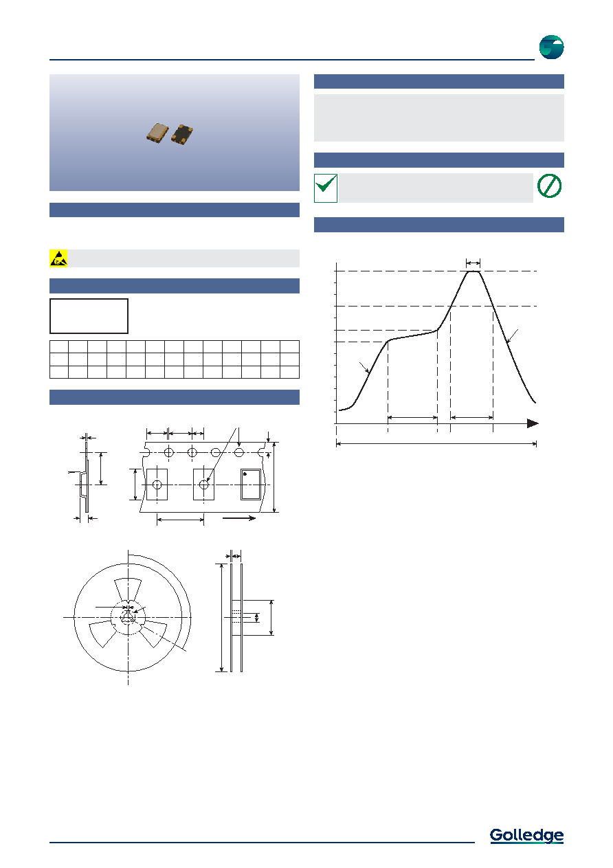
5.00
Ī0.20
3.20
Ī0.20
1.05
Ī0.10
2.60
1.60
1.00
1.60
1.00
1.30
1.30
2.60
SOLDER PAD LAYOUT
1
2
3
4
1
2
4
3
0.70
1.10
PAD
1
2
3
4
CONNECTION
Ground or
Freq adjustment
Ground
Output
Supply
Features
ę
Supply voltages from 2.4V ~ 5.5V
ę
Low power consumption
ę
Miniature SM package
ę
Excellent frequency stability
Product name + variant + option codes + frequency
Option codes must be included to properly specify a model.
eg: GTXO-83V/JS 13.00MHz
Ī2.5ppm -30+75įC, TCXO with VC
GTXO-83T/HN 14.40MHz
Ī2.0ppm -20+70įC, TCXO no VC
Option code X (eg GTXO-83V/X) denotes a custom spec.
Ordering Information
Scale 3:1
Standard Frequencies
Standard.
Optional - Please specify required code(s) when ordering
1: Will operate within specification on any supply voltage from
+2.4V to +5.5V.
2: The output is not DC-free. A coupling capacitor (10nF) may be
required.
Option
Codes
T
V
Variant
Parameters
Specifications
GTXO-83T: TCXO, no frequency adjustment
GTXO-83V: TCXO with VC frequency adjustment
Frequency range: 10.0 ~ 40.0MHz
Frequency stability:
Ī3.0ppm
K
Ī2.5ppm
J
Ī2.0ppm
H
Ī1.5ppm
G
Temperature range:
0 to +50įC
R
-10 to +60įC
C
-20 to +70įC
N
-30 to +75įC
S
Storage temperature range:
-40 to +85įC
Frequency vs supply voltage:
Ī0.2ppm, V
DD
Ī5%
Ageing:
Ī1.0ppm max first year
Supply voltage (V
DD
):
+2.4V ~ +5.5V
(see note 1)
Supply current:
2.0mA max
Output waveform:
Clipped sine, 0.8V p-p
(see note 2)
Test load:
10k
// 10pF
Start up time:
3ms max
Frequency adjustment:
None
Ī8ppm min, +1.5 Ī1.0V
Phase noise (typ @ 20.0MHz):
-54dBc/Hz @ 1Hz
-86dBc/Hz @ 10Hz
-135dBc/Hz @ 1kHz
-151dBc/Hz @ 100kHz
Stability 24hrs after reflow:
Ī1.0ppm max
Preset frequency:
Ī0.5ppm / +25įC Ī2įC
Product Information
GTXO-83
Tel: +44 1460 256 100
Fax: +44 1460 256 101
E-mail: sales@golledge.com
Web: www.golledge.com
28 Mar 2006
Composition
Construction
ę
Ceramic body with gold-plated pads
ę
Metal lid, seam sealed
Tape & Reel Specification
Soldering Profile
200
100
0
įC
Time
5įC/s max
5įC/s max
90s max
40s max
260įC Ī5įC
10s max
Preheat
140~160įC
260
Heat
> 200įC
Slow
cooldown
200s max
Production quantities supplied on T & R, 1k pcs per reel.
Small quantities may be supplied on tape (no reel), or in bulk.
Packaging & Handling
Solder resistance: 260įC x 10 secs x 2.
Pb
Lead
Free
This product is lead-free, and is fully compliant with
the RoHS directive 2002/95/EC
2002/95/EC
RoHS
A
B
C
D
E
F
G
H
J
K
L
M
Y
1
2
3
4
5
6
7
8
9
0
M
Jan Feb Mar Apr May Jun Jul Aug Sep Oct Nov Dec
∑ Pin 1
Marking type: Laser
DC = Date code in YM, eg "CE" = May 2003
Marking
4.0
1.75
12.0
Ī0.2
8.0
3.5
5.5
Ī0.05
2.2
12.4
13ō
180ō
62ō
2.0
20.2ō
120į
MARK
2.0
FEED
+2.0
-0.0
0.3
Ī0.05
5į
5.3
1.5
Ī0.1
1.50ō
Ī0.05
Not to scale. Dimensions in mm. Tolerances Ī0.1mm unless otherwise stated
S83 DC
∑ FREQUENCY
Static sensitive product. Observe proper handling precautions