30.00000
32.00000
33.86880
36.86400
40.00000
44.23680
44.73600
48.00000
49.15200
50.00000
64.00000
66.66600
70.00000
1.8V CMOS Oscillator
GXO-U114G
Tel:
+44 1460 256 100
Fax:
+44 1460 256 101
E-mail:
sales@golledge.com
Web:
www.golledge.com
01 Feb 2002
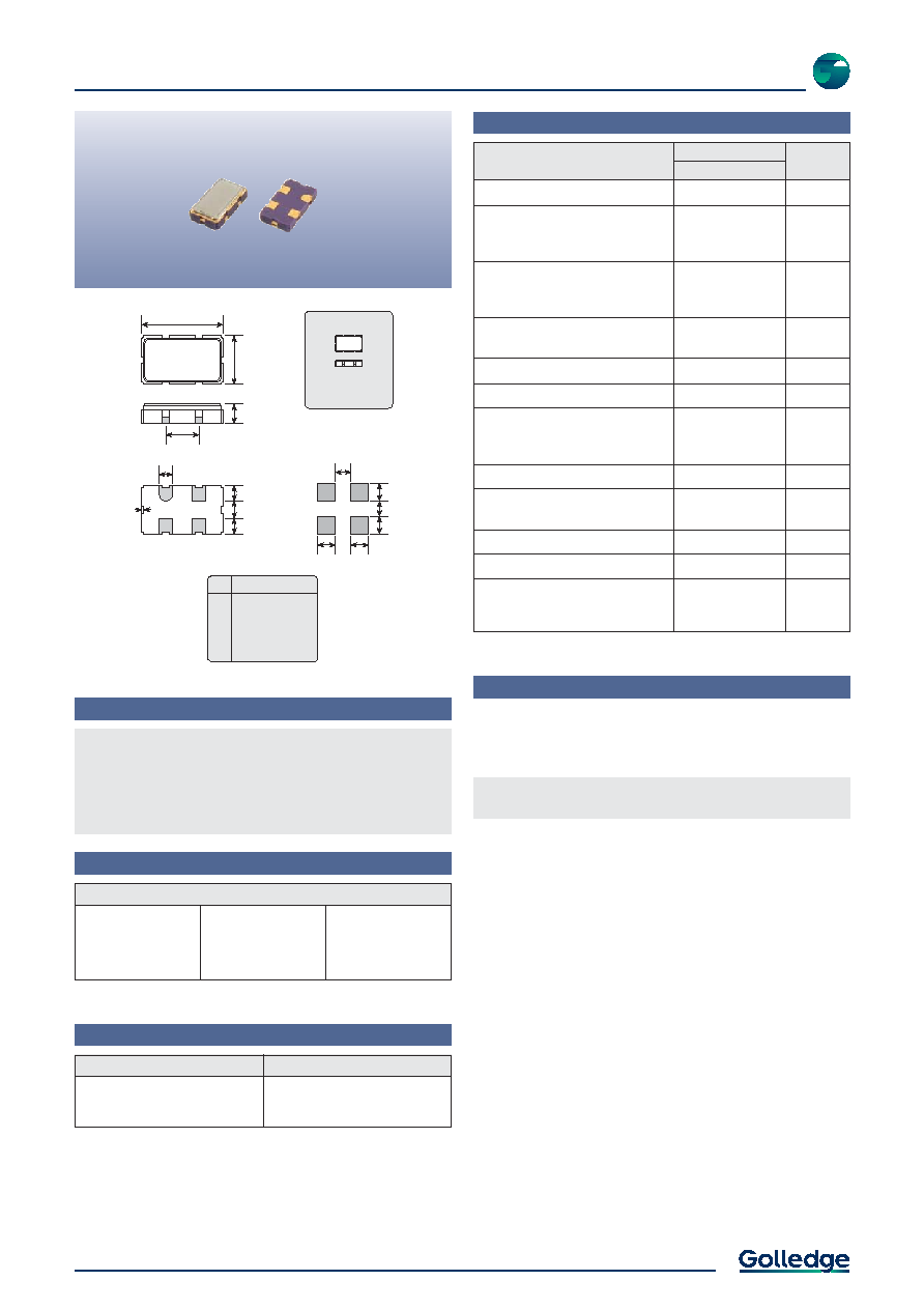
ACTUAL SIZE
PAD
1
2
3
4
CONNECTION
Enable/Disable
Ground
Output
Supply
6.20
(max)
3.70
(max)
1.50
(max)
2.54
0.15
1.00
1.10
1.50
1.10
1
2
3
4
TOP VIEW
4
3
1
2
1.40
1.10
1.40
1.40
1.40
1.10
SOLDER PAD LAYOUT
Features
´
Low voltage and low power consumption
´
Ceramic package with metal lid
´
Enable / disable tristate function
Option
Codes
GXO-U114G
Product
Parameters
Product name + variant + option codes (if any) + frequency
eg:
GXO-U114G 32.0MHz
1.8V, ±100ppm -10+70∞C
GXO-U114G/BI 40.0MHz
1.8V, ±50ppm -40+85∞C
Option code X (eg GXO-U114G/X) denotes a custom spec.
Ordering Information
Frequencies in MHz
Standard Frequencies
Standard.
Optional - Please specify required code(s) when ordering
Scale 3:1
Other frequencies available. Please consult our sales office.
Specifications
Available on T&R - 2k pcs per reel.
Refer to our website for T&R and soldering details.
Frequency range: 30.0 ~ 70.0MHz
Frequency stability:
±100ppm
±50ppm
B
±25ppm
A
Operating temperature range:
-10 to +70∞C
-40 to +85∞C
I
Storage temperature range:
-55 to +125∞C
Supply voltage (V
DD
): +1.8V (±5%)
Supply current:
15mA max
Logic levels:
`0' level = 20%V
DD
max
`1' level = 80%V
DD
min
Start up time:
10ms max
Waveform symmetry:
40:60 max @ 50%V
DD
Driving ability:
15pF HCMOS
Rise / fall time:
3.5ns max
Enable / disable function:
Tristate (control via pad 1)
100ns / 100ns max
Open
`1' level
`0' level
Enabled
Enabled
High Impedance
Enable / Disable Function
Input (pad 1)
Output (pad 3)