HIGH VOLTAGE
POWER SUPPLY UNIT
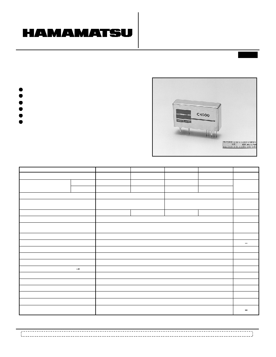
C4900
SERIES
The C4900 series are compact PC≠board mountable high voltage power supplies, especially designed for
photomultiplier tubes. The design offers better performance and improved fail≠safe protection.
The C4900 and≠01 output negative polarity and the C4900≠50 and ≠51 output positive polarity high voltages.
SPECIFICATIONS
FEATURES
Parameter
Unit
C4900
C4900-01
C4900-50
C4900-51
+15
± 1
+12
± 0.5
+15
± 1
+12
± 0.5
14
15
14
15
90
95
90
95
0.6
0.5
0.6
0.5
V
V
mA (Typ.)
% (Typ.)
mA (Max.)
Compact and Lightweight
High stability
Low Power Consumption
Fast Response
Wide Variable Output Range
Ample Protective and Fail≠safe Functions
Input Voltage Range
with no load
with full load
Input Current
a
Output Current
b
Line Regulation against
±1 V or 0.5 V Change
b
± 0.01
% (Typ.)
± 0.01
%/
∞C (Typ.)
± 0.01
mm
∞C
∞C
46
◊ 24 ◊ 12
g
31
0 to +50
-20 to +70
% (Typ.)
V (Typ.)
0.007
k
(Typ.)
80
ms (Typ.)
50
By external controlling voltage (0 V to +5 V) or external potentiometer (50 k
± 2.5 k)
Units protected against reversed power input, reversed/excessive controlling
voltage input, continuous overloading/short circuit in output
+5.13 (with 50 k
external potetiometer)
V (Typ.)
(Controlling voltage
◊ 250) ± 0.5 %
Variable Output Range
0 to ≠1250
0 to +1250
V
≠200 to ≠1250
+200 to +1250
Specification Guaranteed
Output Voltage Range
Load Regulation against
0 % to 100 % Load Change
a
Output Voltage Controlling Modes
Controlling Voltage Input Impedance
Reference Voltage Output
Output Voltage Setting (Absolute value)
Output Voltage Rise Time (0 % 99 %)
b
Operating Temperature Range
b
Storage Temperature Range
Dimensions (W
◊ H ◊ D)
Weight
Protective Functions
Temperature Coefficient
b
a At Maximum Output Voltage.
Ripple / Noise (p-p)
b
b At Maximum Output Voltage and Current.
PATENT
Information furnished by HAMAMATSU is believed to be reliable. However, no responsibility is assumed for possible inaccuracies or omissions. Specifications are
subject to change without notice. No patent rights are granted to any of the circuits described herein. ©2001 Hamamatsu Photonics K.K
Subject to local technical requirements and regulations, availability of products included in this promotional material may vary. Please consult with our sales office.

HIGH VOLTAGE POWER SUPPLY UNIT C4900
SERIES
TACC1013E02
MAY. 2001 IP
Printed in Japan (500)
Figure 1: Output Voltage Controlling
Figure 2: Output Voltage Controlling Characteristic
Figure 3: Example of Ripple/Noise Reduction Circuit
Figure 4: Dimensional Outline (Unit: mm)
Drilling Data for PC Board
(Soldering Face)
*
PATENT: USA No.5548502, 5568343 JAPAN: No.2758552, 2784136 EUROPE: No.641066, 649222
TACCC0049ED
BY EXTERNAL POTENTIOMETER
BY EXTERNAL VOLTAGE
TACCB0043EA
CONTROLLING VOLTAGE (V)
OUTPUT VOLTAGE (V)
5
0
1
+1500
0
+250
+500
+750
+1000
+1250
2
3
4
6
5.3
-1500
0
-250
-500
-750
-1000
-1250
OUTPUT VOLTAGE (V)
(C4900, -01)
(C4900-50, -51)
TACCC0099EB
TACCA0157EB
TACCA0159EB
HAMAMATSU PHOTONICS K.K., Electron Tube Center
314-5, Shimokanzo, Toyooka-village, Iwata-gun, Shizuoka-ken, 438-0193, Japan, Telephone: (81)539/62-5248, Fax: (81)539/62-2205
U.S.A.: Hamamatsu Corporation: 360 Foothill Road, P. O. Box 6910, Bridgewater. N.J. 08807-0910, U.S.A., Telephone: (1)908-231-0960, Fax: (1)908-231-1218 E-mail: usa@hamamatsu.com
Germany: Hamamatsu Photonics Deutschland GmbH: Arzbergerstr. 10, D-82211 Herrsching am Ammersee, Germany, Telephone: (49)8152-375-0, Fax: (49)8152-2658 E-mail: info@hamamatsu.de
France: Hamamatsu Photonics France S.A.R.L.: 8, Rue du Saule Trapu, Parc du Moulin de Massy, 91882 Massy Cedex, France, Telephone: (33)1 69 53 71 00, Fax: (33)1 69 53 71 10 E-mail: infos@hamamatsu.fr
United Kingdom: Hamamatsu Photonics UK Limited: 2 Howard Court, 10 Tewin Road Welwyn Garden City Hertfordshire AL7 1BW, United Kingdom, Telephone: 44-(0)1707-294888, Fax: 44(0)1707-325777 E-mail: info@hamamatsu.co.uk
North Europe: Hamamatsu Photonics Norden AB: Smidesv‰gen 12, SE-171-41 SOLNA, Sweden, Telephone: (46)8-509-031-00, Fax: (46)8-509-031-01 E-mail: info@hamamatsu.se
Italy: Hamamatsu Photonics Italia: S.R.L.: Strada della Moia, 1/E, 20020 Arese, (Milano), Italy, Telephone: (39)02-935 81 733, Fax: (39)02-935 81 741 E-mail: info@hamamatsu.it
HOMEPAGE URL http://www.hamamatsu.com
LOAD
0 V to +5 V*
q
w e
r
t
y
+15 V or +12V
NO
CONNECTION
(IC)
* The instability in the external controlling voltage should be
minimized as it directly affects the output voltage quality.
q
w
e
r
t
y
LOAD
MAX
MIN
50 k
q
w e
r
t
y
+15 V or +12 V
PIN ASSIGNMENT
+15 V or +12 V IN
GND 1 (Input/Output GND)
GND 2 (Controlling Voltage GND)
HV ADJ (Controlling Voltage Input)
Vref OUT (Reference Voltage Output
: 5.13V Typ.)
HV OUT
The housing is internally connected
to pin
w.
Pins
w and e are internally
connected.
+15 V or +12 V
INPUT GND
q
w
y
HV OUT
OUTPUT GND
0.2
µF
(2 kV)
*The ripple/noise can be halved by adding
capacitors as illustrated above.
C4900
SERIES
47
µF
(25 V)
+
46
24
5 MIN.
q
y
9.53
8.25
10.16
2.54
0.5
◊ 0.25
3.81
15.88
15.88
29
1.5
2.5
w e r t
12
0.3
(BOTTOM VIEW)
The mounting tabs can be
bent to the right angle only once
The mounting tabs are solderable.
)
(
MOUNTING TABS
3.81
15.88
15.88
9.53
8.25
10.16
2.54
11.7
4- 2
6- 0.8