 | –≠–ª–µ–∫—Ç—Ä–æ–Ω–Ω—ã–π –∫–æ–º–ø–æ–Ω–µ–Ω—Ç: S5931 | –°–∫–∞—á–∞—Ç—å:  PDF PDF  ZIP ZIP |

NMOS linear image sensors are self-scanning photodiode arrays designed specifically as detectors for multichannel spectroscopy. The scanning
circuit is made up of N-channel MOS transistors, operates at low power consumption and is easy to handle. Each photodiode has a large active
area, high UV sensitivity yet very low noise. The built-in thermoelectric cooler (air cooled) allows a long exposure time achieving a high S/N even
at low light levels. The cap uses a sapphire glass window hermetically welded for high reliability.
Features
l Wide active area
Pixel pitch: 50 µm (S5930 series)
25 µm (S5931 series)
Pixel height: 2.5 mm
l High UV sensitivity with good stability
l Low dark current and high saturation charge allow a long
integration time and a wide dynamic range at room temperature
l Excellent output linearity and sensitivity spatial uniformity
l Start pulse and clock pulses are CMOS logic compatible
l Built-in air-cooled thermoelectric cooler
(setting temperature: 0 ∞C)
Applications
l Multichannel spectrophotometry
l Image readout system
I M A G E S E N S O R
NMOS linear image sensor
Built-in thermoelectric cooler ensures long exposure time and stable operation.
S5930/S5931 series
s
Selection guide
Type No.
Number of pixels
Pixel size
[µm (H) ◊ µm (V)]
Active area size
[mm (H) ◊ mm (V)]
S5930-256S
256
12.8 ◊ 2.5
S5930-512S
512
50 ◊ 2500
25.6 ◊ 2.5
S5931-512S
512
12.8 ◊ 2.5
S5931-1024S
1024
25 ◊ 2500
25.6 ◊ 2.5
In addition to S5930/S5931 series, Hamamatsu provides S8382/S8383 series thermoelectrically cooled NMOS linear image
sensors that offer higher sensitivity in the near IR range. Major characteristics of S8382/S8383 series are almost identical with
S5930/S5931 series except that the peak sensitivity wavelength is 750 nm (see Figure 5) and the saturation charge is 90 m lx s.
NMOS linear image sensor
S5930/S5931 series
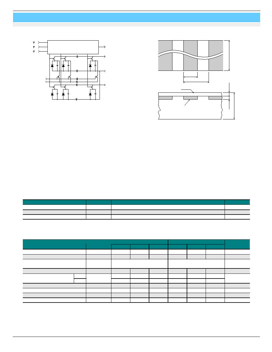
2.5 mm
1.0 µm
1.0 µm
400 µm
OXIDATION SILICON
N TYPE SILICON
P TYPE SILICON
S5930 SERIES: a=50 µm, b=45 µm
S5931 SERIES: a=25 µm, b=20 µm
b
a
KMPDC0020EA
Figure 1 Equivalent circuit
Vss
START
st
CLOCK
CLOCK
1
2
ACTIVE
PHOTODIODE
SATURATION
CONTROL GATE
SATURATION
CONTROL DRAIN
DUMMY DIODE
DUMMY VIDEO
ACTIVE VIDEO
END OF SCAN
DIGITAL SHIFT RESISTER
(MOS SHIFT RESISTER)
Figure 2 Active area structure
KMPDA0132EA
s
Absolute maximum ratings
Parameter
Symbol
Value
Unit
Input pulse (1, 2, st) voltage
V
15
V
Operating temperature *
1
Topr
-40 to +65
∞C
Storage temperature
Tstg
-40 to +85
∞C
*1: No condensation. Ambient temperature should be less than the element cooling temperature +35 ∞C. (Example: Ambient
temperature should be less than 35 ∞C in order to keep the element temperature at 0 ∞C.)
s
Specifications (Ta=25 ∞C, unless otherwise noted)
S5930 series
S5931 series
Parameter
Symbol
Min.
Typ.
Max.
Min.
Typ.
Max.
Unit
Pixel pitch
-
-
50
-
-
25
-
µm
Pixel height
-
-
2.5
-
-
2.5
-
mm
Spectral response range
(10 % of peak)
200 to 1000
200 to 1000
nm
Peak sensitivity wavelength
p
-
600
-
-
600
-
nm
25 ∞C
-
0.2
0.6
-
0.1
0.3
Photodiode dark current *
0 ∞C
I
D
-
0.006
0.018
-
0.003
0.009
pA
Photodiode capacitance *
2
Cph
-
20
-
-
10
-
pF
Saturation exposure *
2,
*
3
Esat
-
180
-
-
180
-
mlx ∑ s
Saturation output charge *
2
Qsat
-
50
-
-
25
-
pC
Photo response non-uniformity *
4
PRNU
-
-
±3
-
-
±3
%
*2: Vb=2.0 V, V=5.0 V
*3: 2856 K, tungsten lamp
*4: 50 % of saturation, excluding the start pixel and last pixel
NMOS linear image sensor
S5930/S5931 series
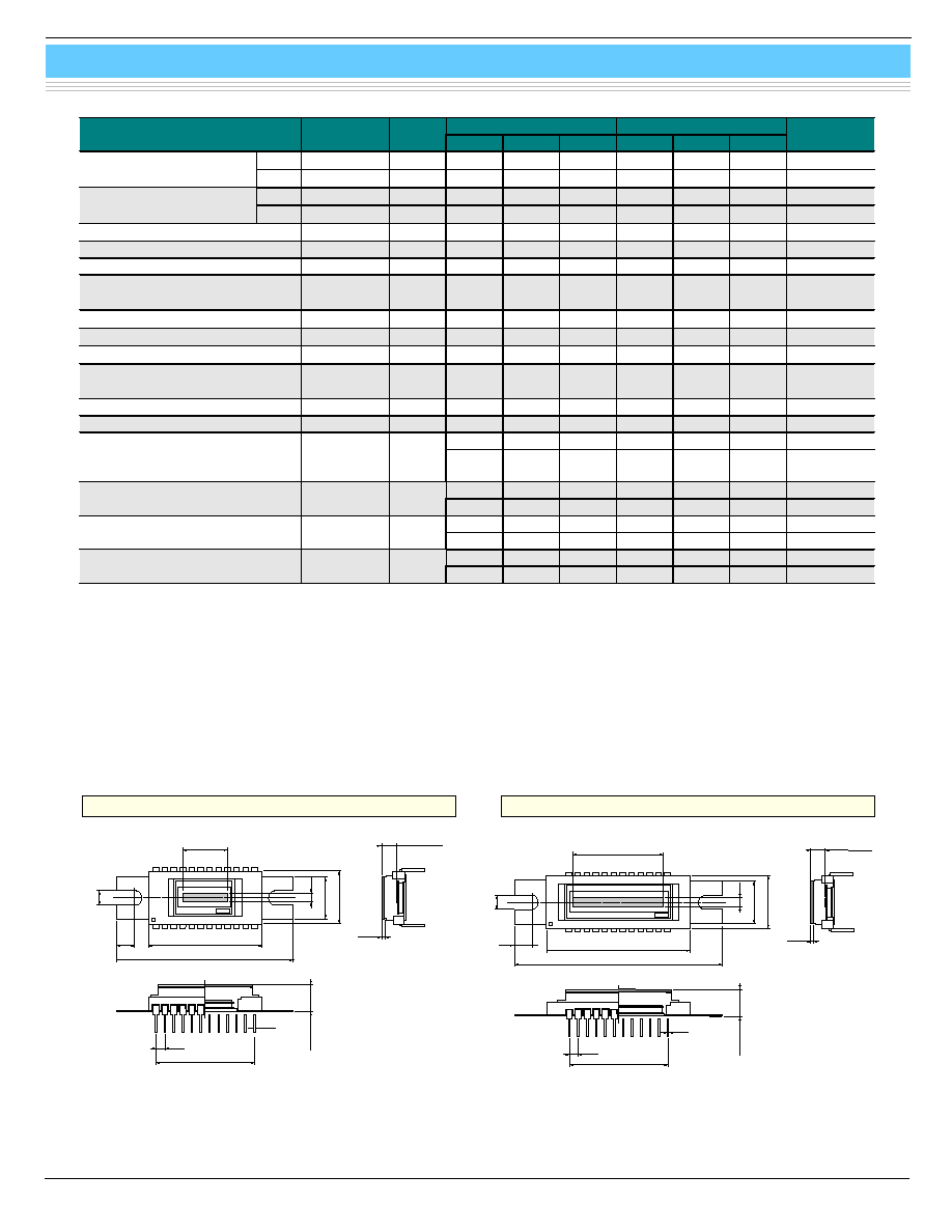
Figure 3 Dimensional outlines (unit: mm)
S5930-256S, S5931-512S
S5930-512S, S5931-1024S
KMPDA0089JA
KMPDA0090JA
32.0 ± 0.3
14.99 ± 0.25
0.46
2.54
27.94
2.5
4.05 ± 0.4 *
2
*1: Thickness of sapphire glass
*2: Distance from the surface of sapphire
glass to the chip surface
12.0
7.65 ± 0.5
50.0
4.0
5.0
0.8 *
1
12.8
25.6
40.64 ± 0.3
14.99 ± 0.25
0.46
2.54
27.94
2.5
12.0
7.65 ± 0.5
4.0
5.0
58.84
4.05 ± 0.4 *
2
0.8 *
1
*1: Thickness of sapphire glass
*2: Distance from the surface of sapphire
glass to the chip surface
s
Electrical characteristics (Ta=25 ∞C)
S5930 series
S5931 series
Parameter
Symbol
Condition
Min.
Typ.
Max.
Min.
Typ.
Max.
Unit
High V1, V2 (H)
4.5
5
10
4.5
5
10
V
Clock pulse (1, 2)
voltage
Low V1, V2 (L)
0
-
0.4
0
-
0.4
V
High
Vs (H)
4.5
V1
10
4.5
V1
10
V
Start pulse (st) voltage
Low
Vs (L)
0
-
0.4
0
-
0.4
V
Video bias voltage *
5
V
b
1.5
V - 3.0 V - 2.5
1.5
V - 3.0 V - 2.5
V
Saturation control gate voltage
Vscg
-
0
-
-
0
-
V
Saturation control drain voltage
Vscd
-
Vb
-
-
Vb
-
V
Clock pulse (1, 2)
rise/fall time *
6
tr1, tr2
tf1, tf2
-
20
-
-
20
-
ns
Clock pulse (1, 2) pulse width
tpw1, tpw2
200
-
-
200
-
-
ns
Start pulse (st) rise/fall time
trs, tfs
-
20
-
-
20
-
ns
Start pulse (st) pulse width
tpws
200
-
-
200
-
-
ns
Start pulse (st) and clock pulse
(2) overlap
tov
200
-
-
200
-
-
ns
Clock pulse space *
6
X
1
, X
2
trf - 20
-
-
trf - 20
-
-
ns
Data rate *
7
f
0.1
-
2000
0.1
-
2000
kHz
-
120 (-256S)
-
-
150 (-512S)
-
ns
Video delay time
tvd
50 % of
saturation
*
7,
*
8
-
160 (-512S)
-
-
200 (-1024S)
-
ns
-
36 (-256S)
-
-
50 (-512S)
-
pF
Clock pulse (1, 2)
line capacitance
C
5 V bias
-
67 (-512S)
-
-
100 (-1024S)
-
pF
-
20 (-256S)
-
-
24 (-512S)
-
pF
Saturation control gate (Vscg)
line capacitance
Cscg
5 V bias
-
35 (-512S)
-
-
45 (-1024S)
-
pF
-
11 (-256S)
-
-
16 (-512S)
-
pF
Video line capacitance
C
V
2 V bias
-
20 (-512S)
-
-
30 (-1024S)
-
pF
*5: V is input pulse voltage.
*6: trf is the clock pulse rise or fall time. A clock pulse space of
rise time/fall time - 20
ns (nanoseconds) or more should be
input if the clock pulse rise or fall time is longer than 20
ns.
*7: Vb=2.0 V, V=5.0 V
*8: Measured with C7883 driver circuit.

NMOS linear image sensor
S5930/S5931 series
0.5
0.4
0.3
0.2
0.1
0
200
400
600
800
1000
1200
WAVELENGTH (nm)
PHOTO SENSITIVITY
(A/W)
(Ta=25 ∞C)
S5930/S5931 SERIES
IR HIGH-SENSITIVITY TYPE
S8382/S8383 SERIES
st
1
2
NC
NC
TE-COOLER +
TE-COOLER -
END OF SCAN
NC
DUMMY VIDEO
ACTIVE VIDEO
Vss
1
2
3
4
5
6
7
8
9
10
11
12
24
23
22
21
20
19
18
17
16
15
14
13
NC
NC
Vss
Vscg
Vsub
NC
THERMISTOR
THERMISTOR
NC
Vscd
NC
NC
Vss, Vsub and NC should be grounded.
Electricity flows between the 20th pin and package metal.
Figure 4 Pin connection
KMPDC0115EA
10
-5
10
2
10
1
10
0
10
-1
10
-2
10
-3
10
-4
10
-3
10
-2
10
-1
10
0
OUTPUT CHARGE (pC)
EXPOSURE (lx ∑ s)
(Typ. Vb=2 V, V =5 V, light source: 2856 K)
SATURATION
CHARGE
S5931 SERIES
SATURATION EXPOSURE
S5930 SERIES
KMPDB0163EA
Figure 5 Spectral response (typical example)
Figure 6 Output charge vs. exposure
KMPDB0164EA
Terminal
Input or output
Description
1, 2
Input
(CMOS logic compatible)
Pulses for operating the MOS shift register. The video data rate is equal
to the clock pulse frequency since the video output signal is obtained
synchronously with the rise of 2 pulse.
st
Input
(CMOS logic compatible)
Pulse for starting the MOS shift register operation. The time interval
between start pulses is equal to the signal accumulation time.
Vss
-
Connected to the anode of each photodiode. This should be grounded.
Vscg
Input
Used for restricting blooming. This should be grounded.
Vscd
Input
Used for restricting blooming. This should be biased at a voltage equal
to the video bias voltage.
Active video
Output
Video output signal. Connects to photodiode cathodes when the
address is on. A positive voltage should be applied to the video line in
order to use photodiodes with a reverse voltage. When the amplitude of
1 and 2 is 5 V, a video bias voltage of 2 V is recommended.
Dummy video
Output
This has the same structure as the active video, but is not connected to
photodiodes, so only spike noise is output. This should be biased at a
voltage equal to the active video or left as an open-circuit when not
needed.
Vsub
-
Connected to the silicon substrate. This should be grounded.
End of scan
Output
(CMOS logic compatible)
This should be pulled up at 5 V by using a 10 k resistor. This is a
negative going pulse that appears synchronously with the 2 timing
right after the last photodiode is addressed.
NC
-
Should be grounded.
TE-cooler
Input
For sensor chip cooling
Thermistor
Output
For temperature control

NMOS linear image sensor
S5930/S5931 series
s
TE-cooler type 1 (T-06E 144P-RNO)characteristics
(built-in S5930-512S, S5931-1024S)
Parameter
Condition
Value
Unit
Built-in resistance
Ta=25 ∞C
1.25
Maximum current
Tc -Th=20 ∞C
3.6
A
Maximum voltage
Tc -Th=80 ∞C
6.2
V
Maximum heat absorption
Tc -Th=20 ∞C
7.5
W
Figure 7 Voltage vs. temperature (Tc=0 ∞C)
KMPDB0165EA
Figure 8 Heat absorption vs. temperature (Tc=0 ∞C)
KMPDB0166EA
Figure 9 Voltage vs. temperature (Tc=20 ∞C)
KMPDB0167EA
Figure 10 Heat absorption vs. temperature (Tc=20 ∞C)
KMPDB0168EA
s
Thermister characteristics
Characteristics
Parameter
Condition
Value
Unit
Resistance
Ta=25 ∞C
10
k
B-constant
3450
k
Operating
temperature
-40 to +100
∫C
Resistance vs. temperature
Temperature (∫C)
Resistance (k)
-20
78.4
-10
46.7
0
28.1
10
18.2
20
12.2
25
10.0
30
8.3
40
5.7
TEMPERATURE (Th - Tc) (∞C)
VOLTAGE (V)
60
80
0
1
5
4
3
2
40
20
0
2.4 A
2.0 A
1.6 A
1.2 A
0.8 A
0.4 A
2.8 A
3.2 A
TEMPERATURE (Th - Tc) (∞C)
HEAT ABSORPTION (W)
60
80
0
2
10
8
6
4
40
20
0
0.4 A
0.8 A
3.2 A
2.8 A
1.2 A
1.6 A
2.0 A
2.4 A
TEMPERATURE (Th - Tc) (∞C)
VOLTAGE (V)
60
80
0
1
5
4
3
2
40
20
0
2.4 A
2.0 A
1.6 A
1.2 A
0.8 A
0.4 A
2.8 A
3.2 A
TEMPERATURE (Th - Tc) (∞C)
HEAT ABSORPTION (W)
60
80
0
2
10
8
6
4
40
20
0
0.4 A
0.8 A
3.2 A
2.8 A
1.2 A
1.6 A
2.0 A
2.4 A

HAMAMATSU PHOTONICS K.K., Solid State Division
1126-1 Ichino-cho, Hamamatsu City, 435-8558 Japan, Telephone: (81) 053-434-3311, Fax: (81) 053-434-5184, http://www.hamamatsu.com
U.S.A.: Hamamatsu Corporation: 360 Foothill Road, P.O.Box 6910, Bridgewater, N.J. 08807-0910, U.S.A., Telephone: (1) 908-231-0960, Fax: (1) 908-231-1218
Germany: Hamamatsu Photonics Deutschland GmbH: Arzbergerstr. 10, D-82211 Herrsching am Ammersee, Germany, Telephone: (49) 08152-3750, Fax: (49) 08152-2658
France: Hamamatsu Photonics France S.A.R.L.: 8, Rue du Saule Trapu, Parc du Moulin de Massy, 91882 Massy Cedex, France, Telephone: 33-(1) 69 53 71 00, Fax: 33-(1) 69 53 71 10
United Kingdom: Hamamatsu Photonics UK Limited: 2 Howard Court, 10 Tewin Road, Welwyn Garden City, Hertfordshire AL7 1BW, United Kingdom, Telephone: (44) 1707-294888, Fax: (44) 1707-325777
North Europe: Hamamatsu Photonics Norden AB: Smidesv‰gen 12, SE-171 41 Solna, Sweden, Telephone: (46) 8-509-031-00, Fax: (46) 8-509-031-01
Italy: Hamamatsu Photonics Italia S.R.L.: Strada della Moia, 1/E, 20020 Arese, (Milano), Italy, Telephone: (39) 02-935-81-733, Fax: (39) 02-935-81-741
Information furnished by HAMAMATSU is believed to be reliable. However, no responsibility is assumed for possible inaccuracies or omissions.
Specifications are subject to change without notice. No patent rights are granted to any of the circuits described herein. ©2001 Hamamatsu Photonics K.K.
NMOS linear image sensor
S5930/S5931 series
Cat. No. KMPD1018E03
Apr. 2001 DN
s
TE-cooler type 2 (T-06E 108P-RNO)characteristics
(built-in S5930-256S, S5931-512S)
Parameter
Condition
Value
Unit
Built-in resistance
Ta=25 ∞C
0.983
Maximum current
Tc -Th=20 ∞C
3.6
A
Maximum voltage
Tc -Th=80 ∞C
4.7
V
Maximum heat absorption
Tc -Th=20 ∞C
5.7
W
Figure 11 Voltage vs. temperature (Tc=0 ∞C)
KMPDB0169EA
Figure 12 Heat absorption vs. temperature (Tc=0 ∞C)
KMPDB0170EA
Figure 13 Voltage vs. temperature (Tc=20 ∞C)
KMPDB0171EA
Figure 14 Heat absorption vs. temperature (Tc=20 ∞C)
KMPDB0172EA
TEMPERATURE (Th - Tc) (∞C)
VOLTAGE (V)
60
80
0
1
5
4
3
2
40
20
0
1.6 A
1.2 A
0.8 A
0.4 A
2.0 A
2.4 A
2.8 A
3.2 A
TEMPERATURE (Th - Tc) (∞C)
VOLTAGE (V)
60
80
0
1
5
4
3
2
40
20
0
1.6 A
1.2 A
0.8 A
0.4 A
2.0 A
2.4 A
2.8 A
3.2 A
TEMPERATURE (Th - Tc) (∞C)
HEAT ABSORPTION (W)
60
80
0
2
10
8
6
4
40
20
0
0.4 A
0.8 A
3.2 A
2.8 A
1.2 A
1.6 A
2.0 A
2.4 A
TEMPERATURE (Th - Tc) (∞C)
HEAT ABSORPTION (W)
60
80
0
2
10
8
6
4
40
20
0
0.4 A
0.8 A
3.2 A
2.8 A
1.2 A
1.6 A
2.0 A
2.4 A