 | –≠–ª–µ–∫—Ç—Ä–æ–Ω–Ω—ã–π –∫–æ–º–ø–æ–Ω–µ–Ω—Ç: S7361 | –°–∫–∞—á–∞—Ç—å:  PDF PDF  ZIP ZIP |

S7361 is a family of FFT-CCD image sensors specifically designed for X-ray imaging. FOS (Fiber Optic plate with Scintillator) that converts X-ray
into visible-light is mounted on a CCD chip, which enables S7361 to do the X-ray imaging.
High performance (resolution & contrast) X-ray imaging is to be realized by using S7361, which allows remarkable reduction with a conventional
X-ray film method.
A trigger signal of controller is to be constituted by using signal, which is detected at X-ray exposure to S7361, as a monitor PD is integrated in a
CCD chip.
S7361 has an effective pixel size of 48 ◊ 48 µm and is available in active area of 28.8 (H) ◊ 19.2 (V) mm
2
.
Features
l Trigger signal fed into controller to be constituted
On-chip photodiode for detecting X-ray irradiation
l Compactness
3.1 mm thickness excluding I/O connector part
l High S/N
12 bit S/N (60 kVp, 30 mR, 0.1 s X-ray irradiation)
l High reliability
Durability for use under 100,000 shots
(60 kVp, 30 mR X-ray irradiation)
l Resolution: 10 Lp/mm
l 600 (H) ◊ 400 (V) pixel format
l Pixel size: 48 ◊ 48 µm
l Coupled with FOS for X-ray imaging
l 100 % fill factor
l Wide dynamic range
l Low dark signal
l Low readout noise
l MPP operation
Applications
l General X-ray imaging
l Non-destructive inspection
I M A G E S E N S O R
CCD area image sensor
Front-illuminated FFT-CCDs for X-ray imaging
S7361
I Selection guide
Type No.
Cooling
Number of
total pixels
Number of active
pixels
Active area
[mm (H) ◊ mm (V)]
S7361
Non-cooled
608 ◊ 402
600 ◊ 400
28.8 ◊ 19.2
Note) As an input window, FOS is suited to S7361.
I General ratings
Parameter
Specification
CCD structure
Full frame transfer
Fill factor
100 %
Number of active pixels
600 (H) ◊ 400 (V)
Pixel size
48 (H) ◊ 48 (V) µm
Active area
28.8 (H) ◊ 19.2 (V) mm
Vertical clock phase
2 phase
Horizontal clock phase
2 phase
Output circuit
One-stage MOSFET source follower without load resistance
Package
Ceramic package
Window
FOS (Fiber Optic plate with Scintillator)
1

CCD area image sensor
S7361
I Absolute maximum ratings (Ta=25 ∞C)
Parameter
Symbol
Min.
Typ.
Max.
Unit
Storage temperature
Tstg
-10
-
+70
∞C
Operating temperature
Topr
0
-
+40
∞C
OD voltage
V
OD
-0.5
-
+25
V
RD voltage
V
RD
-0.5
-
+18
V
SG voltage
V
SG
-10
-
+15
V
OG voltage
V
OG
-10
-
+15
V
RG voltage
V
RG
-10
-
+15
V
TG voltage
V
TG
-10
-
+15
V
Vertical clock voltage
V
P1V
, V
P2V
-10
-
+15
V
Horizontal clock voltage
V
P1H
, V
P2H
-10
-
+15
V
I Operating conditions (MPP mode, Ta=25 ∞C)
Parameter
Symbol
Min.
Typ.
Max.
Unit
Output transistor drain voltage
V
OD
12
15
18
V
Reset drain voltage
V
RD
11.5
12
12.5
V
Output gate voltage
V
OG
1
3
5
V
Substrate voltage
V
SS
-
0
-
V
High
V
P1VH
, V
P2VH
4
6
8
Vertical shift register
clock voltage
Low
V
P1VL
, V
P2VL
-9
-8
-7
V
High
V
P1HH
, V
P2HH
4
6
8
Horizontal shift register
clock voltage
Low
V
P1HL
, V
P2HL
-9
-8
-7
V
High
V
SGH
4
6
8
Summing gate voltage
Low
V
SGL
-9
-8
-7
V
High
V
RGH
4
6
8
Reset gate voltage
Low
V
RGL
-9
-8
-7
V
High
V
TGH
4
6
8
Transfer gate voltage
Low
V
TGL
-9
-8
-7
V
I Electrical characteristics (Ta=25 ∞C)
Parameter
Symbol
Remark
Min.
Typ.
Max.
Unit
Signal output frequency
fc
-
1
2
MHz
Reset clock frequency
frg
-
1
2
MHz
Vertical shift register capacitance
C
P1V
, C
P2V
-
25000
-
pF
Horizontal shift register capacitance
C
P1H
, C
P2H
-
1200
-
pF
Summing gate capacitance
C
SG
-
20
-
pF
Reset gate capacitance
C
RG
-
10
-
pF
Transfer gate capacitance
C
TG
-
400
-
pF
Transfer efficiency
CTE
*
1
0.99995
0.99999
-
-
DC output level
Vout
*
2
3
6
9
V
Output impedance
Zo
*
2
-
1000
-
W
Power dissipation
P
*
2,
*
3
-
60
-
mW
*1: Measured at half of the full well capacity. CTE is defined per pixel.
*2: V
OD
=15 V, R
L
(load resistance of source follower) =1 kW.
*3: Power dissipation of the on-chip amplifier.
2
CCD area image sensor
S7361
......
......
1
2
3
596
597
598
599
600
23
399
398
400
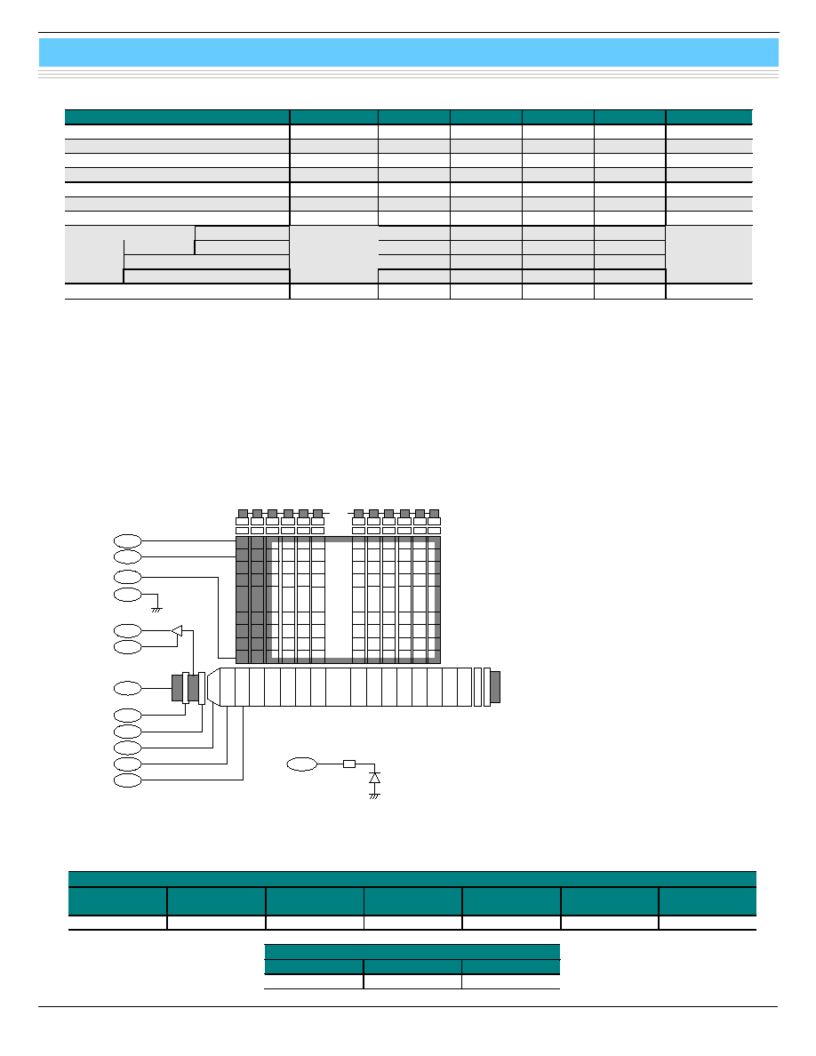
D1
D2
S1
S2
S3
S4
S5
S6
S599
S600
S601
S602
S603
S604
D3
D4
......
P1V
P2V
TG
SS
OS
OD
RD
RG
OG
SG
P1H
P2H
V-
MONITORING PHOTODIODE
13
1
2
3
4
5
6
7
8
9
12
10
11
I Electrical and optical characteristics (Ta=25 ∞C, unless otherwise noted)
Parameter
Symbol
Remark
Min.
Typ.
Max.
Unit
Saturation output voltage
Vsat
-
Fw ◊ Sv
-
V
Full well capacity
Fw
600
1200
-
ke
-
CCD node sensitivity
Sv
*
4
0.25
0.4
-
µV/e
-
Dark signal (MPP mode)
DS
*
5
-
8
24
ke
-
/pixel/s
Readout noise
Nr
*
6
-
80
160
e
-
rms
Dynamic range
DR
*
7
-
15,000
-
-
X-ray response non-uniformity
XRNU
*
8,
*
9
-
±20
±30
%
White spots
-
-
10
Point
defects *
10
Black spots
-
-
10
Cluster defects
*
11
-
-
0
Blemish
Column defects
-
*
12
-
-
0
-
X-ray resolution
DR
*
8
8
10
-
Lp/mm
*4: V
OD
=15 V, R
L
(load resistance of source follower) = 1 kW.
*5: Dark signal doubles for every 5 to 7 ∞C.
*6: -40 ∞C, operating frequency is 1 MHz.
*7: Dynamic range = Full well capacity / Readout noise
*8: X-ray irradiation of 60 kVp, measured at half of the full well capacity.
*9: XRNU (%) = Noise / Signal ◊ 100
Noise: Fixed pattern noise (peak to peak)
In the range that excludes 5 pixels from edges to the center at every position.
*10: White spots > 20 times of typ. dark signal (8 ke
-
/pixel/s).
Black spots > 50 % reduction in response relative to adjacent pixels, measured at half of the full well capacity.
*11: continuous 2 to 9 point defects.
*12: continuous >10 point defects.
I Device structure
KMPDC0114EA
I Pixel format
¨ Left Horizontal Direction Æ Right
Blank
Optical
black
Isolation
Effective
Isolation
Optical
black
Blank
2
2
1
600
1
0
2
Top ¨ Vertical direction Æ Bottom
Isolation
Effective
Isolation
1
400
1
3
CCD area image sensor
S7361
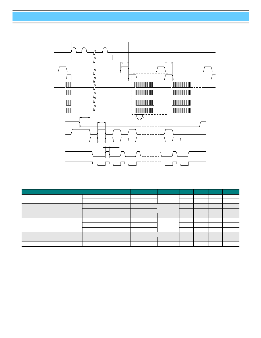
I Timing chart
Parameter
Symbol
Remark
Min.
Typ.
Max.
Unit
Pulse width
tpwv
30
-
-
µs
P1V,P2V,TG
Rise and fall time
tprv, tpfv
*
13
200
-
-
ns
Pulse width
tpwh
250
-
-
ns
Rise and fall time
tprh, tpfh
10
-
-
ns
P1H,P2H
Duty ratio
*
13
-
50
-
%
Pulse width
tpws
250
-
-
ns
Rise and fall time
tprs, tpfs
10
-
-
ns
SG
Duty ratio
-
50
-
%
Pulse width
tpwr
10
-
-
ns
RG
Rise and fall time
tprr, tpfr
5
-
-
ns
TG-P1H
Overlap time
tovr
18
-
-
µs
*13: Symmetrical pulses should be overlapped at 50 % of maximum amplitude.
X-RAY
EXPOSURE
Trigger *
1
P1V
P2V, TG *
2
P1H
P2H, SG
RG
OUT
*1: Low active trigger pulse
*2: TG terminal can be short-circuited to P2V terminal.
P2V, TG
P1H
P2H, SG
RG
OUT
Tpwv
INTEGRATION PERIOD
READOUT PERIOD
Tpwv
1
VD1
2, 3, ... , 399, 400, VD2
VD: VERTICAL DUMMY
ENLARGED VIEW
Tovr
Tpwh, Tpws
Tpwr
D1
D2
S1
S2, S3, S4, ... , S602, S603, S604
D3
D4
KMPDC0113EA
4
CCD area image sensor
S7361
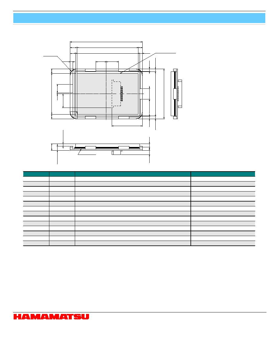
sional outline ( 7361, unit: mm)
14.4 ± 0.5
(5
◊
) (5.0)
6.55 ± 0.5
19.2
2.15
2.15
(4.0)
(0.5)
(5.75)
(1.2)
2.0
(1.2)
(1.2)
FOP
1.5
(2.0)
3.1 ± 0.3
2.0 ± 0.3
1.1 ± 0.3
(1.325)
(4.85)
(1.3)
(4 ◊) R3.5
FOP
30.2
ACTIVE AREA
28.8
(2.6)
3.2
FOP
20.85
(1.325)
23.5 ± 0.3
34.0 ± 0.4
molex
52745-1417
Cu-w (0.5 t)
14
1
KMPDA0128EA
I Pin connections
Pin No.
Symbol
Description
Remark
1
P1V
CCD vertical register clock-1
2
P2V
CCD vertical register clock-2
3
TG
Transfer gate
Same timing as P2V
4
SS
Substrate
5
OS
Output transistor source
6
OD
Output transistor drain
7
RD
Reset drain
8
RG
Reset gate
9
OG
Output gate
10
P1H
CCD horizontal register clock-1
11
P2H
CCD horizontal register clock-2
12
SG
Summing gate
Same timing as P2H
13
V-
Monitor PD cathode
Anode is shorted to SS
14
NC
I Precautions for use
(Electrostatic countermeasures)
*Handle these sensors with bare hands or wearing cotton gloves. In addition, wear anti-static clothing or use a wrist band with
an earth ring, in order to prevent electrostatic damage due to electrical charges from friction.
*Avoid directly placing these sensors on a work-desk or work-bench that may carry an electrostatic charge.
*Provide ground lines or ground connection with the work-floor, work-desk and work-bench to allow static electricity to dis-
charge.
*Ground the tools used to handle these sensors, such as tweezers and soldering irons.
It is not always necessary to provide all the electrostatic measures stated above. Implement these measures according to
the amount of damage that occurs.
I Dimensional outline (unit: mm)
HAMAMATSU PHOTONICS K.K., Solid State Division
1126-1 Ichino-cho, Hamamatsu City, 435-8558 Japan, Telephone: (81) 053-434-3311, Fax: (81) 053-434-5184, http://www.hamamatsu.com
U.S.A.: Hamamatsu Corporation: 360 Foothill Road, P.O.Box 6910, Bridgewater, N.J. 08807-0910, U.S.A., Telephone: (1) 908-231-0960, Fax: (1) 908-231-1218
Germany: Hamamatsu Photonics Deutschland GmbH: Arzbergerstr. 10, D-82211 Herrsching am Ammersee, Germany, Telephone: (49) 08152-3750, Fax: (49) 08152-2658
France: Hamamatsu Photonics France S.A.R.L.: 8, Rue du Saule Trapu, Parc du Moulin de Massy, 91882 Massy Cedex, France, Telephone: 33-(1) 69 53 71 00, Fax: 33-(1) 69 53 71 10
United Kingdom: Hamamatsu Photonics UK Limited: 2 Howard Court, 10 Tewin Road, Welwyn Garden City, Hertfordshire AL7 1BW, United Kingdom, Telephone: (44) 1707-294888, Fax: (44) 1707-325777
North Europe: Hamamatsu Photonics Norden AB: Smidesv‰gen 12, SE-171 41 Solna, Sweden, Telephone: (46) 8-509-031-00, Fax: (46) 8-509-031-01
Italy: Hamamatsu Photonics Italia S.R.L.: Strada della Moia, 1/E, 20020 Arese, (Milano), Italy, Telephone: (39) 02-935-81-733, Fax: (39) 02-935-81-741
Information furnished by HAMAMATSU is believed to be reliable. However, no responsibility is assumed for possible inaccuracies or omissions.
Specifications are subject to change without notice. No patent rights are granted to any of the circuits described herein. ©2003 Hamamatsu Photonics K.K.
Cat. No. KMPD1046E02
Feb. 2003 DN
5