P H O T O D I O D E
PRELIMINARY DATA
Jan. 2001
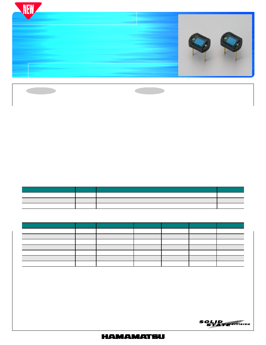
S8265
Si photodiode
Visible sensitivity photodiode with high humidity resistance
Features
l
High humidity resistance (85 ∞C, 85 %, 1000 h)
l
Visible-compensation filter
l
Ceramic package (6 ◊ 8 mm)
l
Active area: 2.8 ◊ 2.4 mm
Applications
l
Light dimmer in locations at high humidity or for outdoor use
s
Absolute maximum ratings (Ta=25 ∞C)
Parameter
Symbol
Value
Unit
Reverse voltage
V
R
Max.
10
V
Operating temperature
Topr
-25 to +85
∞
C
Storage temperature
Tstg
-40 to +85
∞
C
s
Electrical and optical characteristics (Ta=25 ∞C)
Parameter
Symbol
Condition
Min.
Typ.
Max.
Unit
Spectral response range
-
340 to 720
-
nm
Peak sensitivity wavelength
p
-
540
-
nm
Photo sensitivity
S
=
p
-
0.3
-
A/W
Short circuit current
Isc
100 lx , 2856 K
0.40
0.52
-
µ
A
Dark current
I
D
V
R
=1 V
-
3
20
pA
Rise time
tr
V
R
=0 V, R
L
=1 k
-
0.5
-
µ
s
Terminal capacitance
Ct
V
R
=0 V, f=10 kHz
-
230
-
pF
Si photodiode
S8265
8.0
CATHODE
TERMINAL MARK
6.0
0.7
9 ± 1
1.5 ± 0.2
5.0 ± 0.2
0.45
+0
- 0.25
+
0.1
-
0.3
ACTIVE AREA
PHOTOSENSITIVE
SURFACE
FILTER
0.45
LEAD
KSPDB0164EA
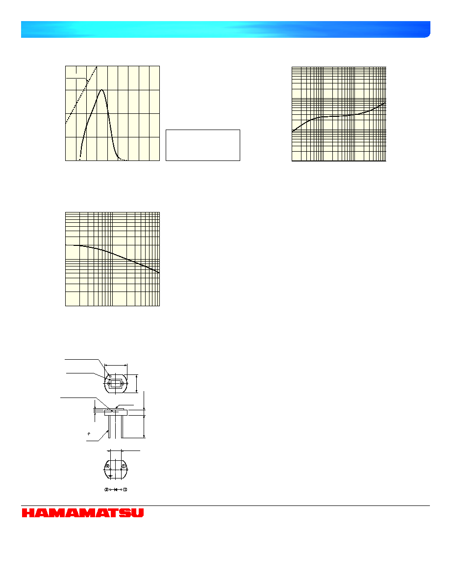
s
Dark current vs. reverse voltage
s
Terminal capacitance vs. reverse voltage
s
Dimensional outline (unit: mm)
KSPDA0127EA
0
0.1
0.2
0.3
0.4
200
400
600
800
1000
WAVELENGTH (nm)
PHOTO SENSITIVITY
(A/W)
(Typ. Ta=25 ∞C)
QE=100%
100 fA
100 pA
10 pA
1 pA
0.01
0.1
1
10
(Typ. Ta=25 ∞C)
REVERSE VOLTAGE (V)
DARK CURRENT
10 pF
0.1
1
10
(Typ. Ta=25 ∞C)
100 pF
1 nF
TERMINAL CAPACITANCE
REVERSE VOLTAGE (V)
KSPDB0170EA
KSPDB0171EA
Almost no decrease in
photo sensitivity even after
1000 hours of operation at
85 ∞C and RH 85 %
s
Spectral response
HAMAMATSU PHOTONICS K.K., Solid State Division
1126-1 Ichino-cho, Hamamatsu City, 435-8558 Japan, Telephone: (81) 053-434-3311, Fax: (81) 053-434-5184, http://www.hamamatsu.com
U.S.A.: Hamamatsu Corporation: 360 Foothill Road, P.O.Box 6910, Bridgewater, N.J. 08807-0910, U.S.A., Telephone: (1) 908-231-0960, Fax: (1) 908-231-1218
Germany: Hamamatsu Photonics Deutschland GmbH: Arzbergerstr. 10, D-82211 Herrsching am Ammersee, Germany, Telephone: (49) 08152-3750, Fax: (49) 08152-2658
France: Hamamatsu Photonics France S.A.R.L.: 8, Rue du Saule Trapu, Parc du Moulin de Massy, 91882 Massy Cedex, France, Telephone: 33-(1) 69 53 71 00, Fax: 33-(1) 69 53 71 10
United Kingdom: Hamamatsu Photonics UK Limited: 2 Howard Court, 10 Tewin Road, Welwyn Garden City, Hertfordshire AL7 1BW, United Kingdom, Telephone: (44) 1707-294888, Fax: (44) 1707-325777
North Europe: Hamamatsu Photonics Norden AB: Smidesv‰gen 12, SE-171 41 Solna, Sweden, Telephone: (46) 8-509-031-00, Fax: (46) 8-509-031-01
Italy: Hamamatsu Photonics Italia S.R.L.: Strada della Moia, 1/E, 20020 Arese, (Milano), Italy, Telephone: (39) 02-935-81-733, Fax: (39) 02-935-81-741
Information furnished by HAMAMATSU is believed to be reliable. However, no responsibility is assumed for possible inaccuracies or omissions.
Specifications are subject to change without notice. No patent rights are granted to any of the circuits described herein. ©2001 Hamamatsu Photonics K.K.
Cat. No. KSPD1041E01
Jan. 2001 DN