 | –≠–ª–µ–∫—Ç—Ä–æ–Ω–Ω—ã–π –∫–æ–º–ø–æ–Ω–µ–Ω—Ç: S8655 | –°–∫–∞—á–∞—Ç—å:  PDF PDF  ZIP ZIP |
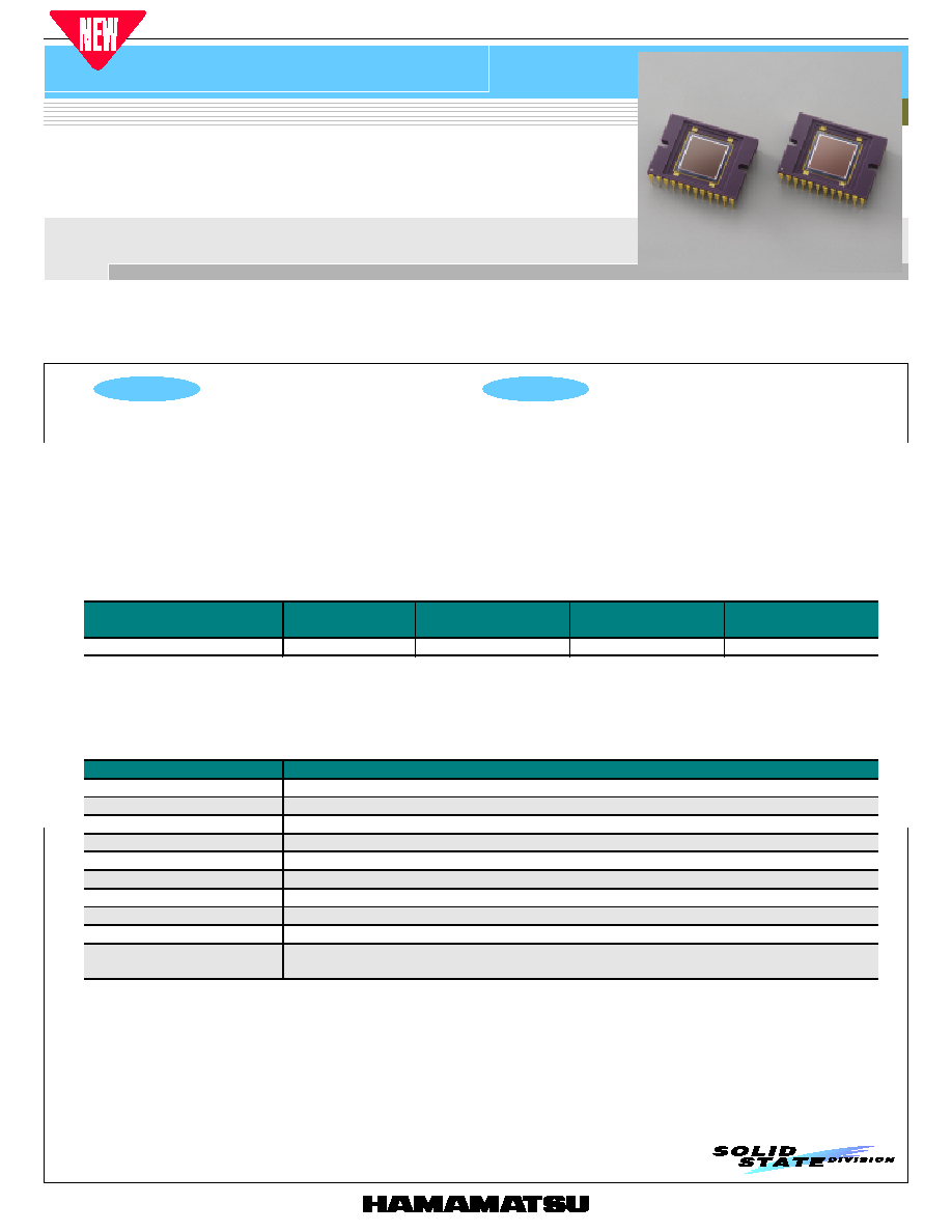
S8655
S8655 is a FFT-CCD area image sensor specifically designed for low-light-level detection in scientific applications. In particular, this image sensor
is ideally suited for extremely low-light-level detection in such fields as spectroscopy and astronomy.
By operating this image sensor in MPP mode, the dark signal can be exceedingly reduced. Moreover, use of the low-noise readout amplifier
enables low-light-level detection and long integration time, thus achieving a wide dynamic range.
S8655 has an effective pixel size of 12 ◊ 12 µm and is available in active area of 12.288 (H) ◊ 12.288 (V) mm.
Features
l 1024 (H) ◊ 1024 (V) pixel format
l Pixel size: 12 ◊ 12 µm
l 100 % fill factor
l Wide dynamic range
l Low dark current
l Low readout noise
l MPP operation
Applications
l Astronomy
l Scientific measuring instrument
l Fluorescence spectrometer
l Raman spectrophotometer
l Optical and spectrophotometric analyzer
l For low-light-level detection requiring
I M A G E S E N S O R
CCD area image sensor
1024 ◊ 1024 pixels, front-illuminated FFT-CCD
PRELIMINARY DATA
Jan. 2002
I Selection and order guide
Type No.
Cooling
Number of
total pixels
Number of
active pixels
Active area
[mm (H) ◊ mm (V)]
S8655
Non-cooled
1044 ◊ 1032
1024 ◊ 1024
12.288 ◊ 12.288
A window material can be selected upon need, and the following is available.
Temporary window (standard) : expressed by N #
# This should be added at the end of a type No. when ordered.
ex. S8655N: temporary window
I General ratings
Parameter
Specification
CCD structure
Full frame transfer
Fill factor
100 %
Number of active pixels
1024 (H) ◊ 1024 (V)
Pixel size
12 (H) ◊ 12 (V) µm
Active area
12.288 (H) ◊ 12.288 (V) mm
Vertical clock phase
2 phase
Horizontal clock phase
2 phase
Output circuit
One-stage MOSFET source follower for low noise readout
Package
24 pin ceramic DIP
Window
Temporary window (standard)
FOP is available upon request
1

CCD area image sensor
S8655
2
I Absolute maximum ratings (Ta=25 ∞C)
Parameter
Symbol
Min.
Typ.
Max.
Unit
Operating temperature
Topr
-50
-
+30
∞C
Storage temperature
Tstg
-50
-
+70
∞C
OD voltage
V
OD
-0.5
-
+25
V
RD voltage
V
RD
-0.5
-
+18
V
ISV voltage
V
ISV
-0.5
-
+18
V
ISH voltage
V
ISH
-0.5
-
+18
V
IGV voltage
V
IG1V
, V
IG2V
-10
-
+15
V
IGH voltage
V
IG1H
, V
IG2H
-10
-
+15
V
SG voltage
V
SG
-10
-
+15
V
OG voltage
V
OG
-10
-
+15
V
RG voltage
V
RG
-10
-
+15
V
TG voltage
V
TG
-10
-
+15
V
Vertical clock voltage
V
P1V
, V
P2V
-10
-
+15
V
Horizontal clock voltage
V
P1H
, V
P2H
-10
-
+15
V
I Operating conditions (MPP mode, Ta=25 ∞C)
Parameter
Symbol
Min.
Typ.
Max.
Unit
Output transistor drain voltage
V
OD
18
20
22
V
Reset drain voltage
V
RD
11.5
12
12.5
V
Output gate voltage
V
OG
1
3
5
V
Substrate voltage
V
SS
-
0
-
V
Test point (vertical input source)
V
ISV
-
V
RD
-
V
Test point (horizontal input source)
V
ISH
-
V
RD
-
V
Test point (vertical input gate)
V
IG1V
, V
IG2V
-8
0
-
V
Test point (horizontal input gate)
V
IG1H
, V
IG2H
-8
0
-
V
High
V
P1VH
, V
P2VH
4
6
8
Vertical shift register
clock voltage
Low
V
P1VL
, V
P2VL
-9
-8
-7
V
High
V
P1HH
, V
P2HH
4
6
8
Horizontal shift register
clock voltage
Low
V
P1HL
, V
P2HL
-9
-8
-7
V
High
V
SGH
4
6
8
Summing gate voltage
Low
V
SGL
-9
-8
-7
V
High
V
RGH
4
6
8
Reset gate voltage
Low
V
RGL
-9
-8
-7
V
High
V
TGH
4
6
8
Transfer gate voltage
Low
V
TGL
-9
-8
-7
V
I Electrical characteristics (Ta=25 ∞C)
Parameter
Symbol
Min.
Typ.
Max.
Unit
Signal output frequency
fc
-
-
1
MHz
Vertical shift register capacitance
C
P1V
, C
P2V
-
6,000
-
pF
Horizontal shift register capacitance
C
P1H
, C
P2H
-
200
-
pF
Summing gate capacitance
C
SG
-
5
-
pF
Reset gate capacitance
C
RG
-
5
-
pF
Transfer gate capacitance
C
TG
-
50
-
pF
Charge transfer efficiency *
1
C
TE
0.99995
0.99999
-
-
DC output level *
2
Vout
12
15
18
V
Output impedance *
2
Zo
-
3
-
kW
Power consumption *
2
*
3
P
-
15
-
mW
*1: Charge transfer efficiency per pixel, measured at half of the full well.
*2: The values depend on the load resistance. (typical, VOD=20 V, load resistance=22 kW)
*3: Power consumption of the on-chip amplifier.
CCD area image sensor
S8655
3
I Electrical and optical characteristics (Ta=25 ∞C, unless otherwise noted)
Parameter
Symbol
Remark
Min.
Typ.
Max.
Unit
Saturation output voltage
Vsat
-
-
Fw ◊ Sv
-
V
Vertical
-
60
-
Full well capacity
Horizontal
Fw
-
-
72
-
ke
-
CCD node sensitivity
Sv
*
4
-
2.8
-
µV/e
-
25 ∞C
-
200
-
Dark current
(MPP mode)
0 ∞C
DS
*
5
-
10
-
e
-
/pixel/s
Readout noise
Nr
*
6
-
4
8
e
-
rms
Dynamic range (area scanning)
DR
*
7
-
15,000
-
-
Spectral response range
l
-
-
400 to 1100
-
nm
Photo response non-uniformity
PRNU
*
8
-
-
±10
%
Point defect
*
9
-
-
10
Cluster defect
*
10
-
-
0
Blemish
(grade: 0 *
12
)
Column defect
-
*
11
-
-
0
-
*4: V
OD
=20 V, load resistance=22 kW.
*5: Dark current nearly doubles for every 5 to 7 ∞C increase in temperature.
*6: -40 ∞C, operating frequency is 80 kHz.
*7: Dynamic range DR=Full well capacity/Readout noise
*8: Measured at half of the full well capacity output.
*9: White spots > 3 % of full well at 0 ∞C after Ts=1 s, Black spots > 50 % reduction in response relative to adjacent pixels.
*10: Continuous 2 to 9 point defects.
*11: Continuous ≥ 10 point defects.
*12: Please make contact with sales office about other grades.
Fixed pattern noise (peak to peak)
Signal
◊ 100
Photo response non-uniformity (PRNU) [%] =
I Pin connections
Pin No.
Symbol
Description
Remark
1
RG
Reset gate
-
2
RD
Reset drain
-
3
OS
Output source
-
4
OD
Output transistor drain
-
5
OG
Output gate
-
6
SG
Summing gate
-
7
P2H
CCD horizontal register clock-2
-
8
NC
No connection
-
9
P1H
CCD horizontal register clock-1
-
10
NC
No connection
-
11
IG2H
Test point (horizontal input gate-2)
Shorted to ground
12
IG1H
Test point (horizontal input gate-1)
Shorted to ground
13
ISH
Test point (horizontal input source)
Shorted to RD
14
TG
Transfer gate
-
15
P2V
CCD vertical register clock-2
-
16
NC
No connection
-
17
P1V
CCD vertical register clock-1
-
18
NC
No connection
-
19
NC
No connection
-
20
SS
Substrate (ground)
-
21
NC
No connection
-
22
ISV
Test point (vertical input source)
Shorted to RD
23
IG2V
Test point (vertical input gate-2)
Shorted to ground
24
IG1V
Test point (vertical input gate-1)
Shorted to ground

CCD area image sensor
S8655
4
1.27
3.0
2.4
12.288
22.73 ± 0.3
23.11 ± 0.3
22.86 ± 0.3
1.3 ± 0.3
2.54
30.48 ± 0.3
ACTIVE AREA
12.288
27.0
R1.2
PHOTOSENSITIVE
SURFACE
50
40
30
20
10
0
400
500
600
700
WAVELENGTH (nm)
800
900
1000 1100 1200
QUANTUM EFFICIENCY (%)
(Typ. Ta=25 ∞C)
KMPDB0051EA
I Spectral response without window
KMPDA0140EA
I Dimensional outline (unit: mm)

CCD area image sensor
S8655
KMPDC0155EA
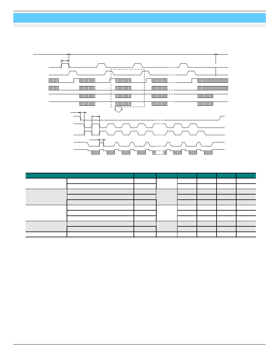
I Device structure, line output format
5
......
......
......
H
IG1V IG2V ISV
SS
RG
RD
OS
OD
OG
SG
D1
D2
D3
D4
D5
D6
D7
D8
D9
D10
D11
D12
D13
D14
D15
D16
D17
D18
D19
D20
1
2
3
4
5
6
20
23
22
24
14
17
V=1024
H=1024
ISH
IG1H
IG2H
P1H
P2H
13
12
11
9
7
4 BLANK
4 BLANK
4 OPTICAL
BLACK
4 ISOLATION
1024
SIGNAL OUT
4 ISOLATION
TG
P1V
15
P2V
1
V
Pixel format
Left ¨ Horizontal direction Æ Right
Blank
Optical black
Isolation
Effective
Isolation
Optical black
Blank
4
4
4
1024
4
-
4
Top ¨ Vertical direction Æ Bottom
Isolation
Effective
Isolation
4
1024
4
CCD area image sensor
S8655
6
Parameter
Symbol
Remark
Min.
Typ.
Max.
Unit
Pulse width
Tpwv
6
-
-
µs
P1V
P2V, TG
Rise and fall time
Tprv, Tpfv
*
13
200
-
-
ns
Pulse width
Tpwh
500
-
-
ns
Rise and fall time
Tprh, Tpfh
10
-
-
ns
P1H, P2H
Duty ratio
-
*
13
-
50
-
%
Pulse width
Tpws
500
-
-
ns
Rise and fall time
Tprs, Tpfs
10
-
-
ns
SG
Duty ratio
-
-
-
50
-
%
Pulse width
Tpwr
100
-
-
ns
RG
Rise and fall time
Tprr, Tpfr
-
5
-
-
ns
TG P1H
Overlap time
Tovr
-
3
-
-
µs
*13: Symmetrical pulses should be overlapped at 50 % of maxmum amplitude.
KMPDC0156EA
I Timing chart
G Area scanning 1 (low dark current mode)
INTEGRATION PERIOD
(Shutter must be open)
P1V
RG
OS
P2V, TG
P1H
P2H, SG
READOUT PERIOD (Shutter must be closed)
ENLARGED VIEW
4..1031
Tpwv
Tovr
Tpwr
D1
D2
D3
D4
D18
D19
D20
D5..D12, S1..S1024, D13..D17
P2V, TG
P1H
P2H, SG
RG
OS
Tpwh, Tpws
1
2
3
1032
1024+8 (ISOLATION)

CCD area image sensor
S8655
7
HAMAMATSU PHOTONICS K.K., Solid State Division
1126-1 Ichino-cho, Hamamatsu City, 435-8558 Japan, Telephone: (81) 053-434-3311, Fax: (81) 053-434-5184, http://www.hamamatsu.com
U.S.A.: Hamamatsu Corporation: 360 Foothill Road, P.O.Box 6910, Bridgewater, N.J. 08807-0910, U.S.A., Telephone: (1) 908-231-0960, Fax: (1) 908-231-1218
Germany: Hamamatsu Photonics Deutschland GmbH: Arzbergerstr. 10, D-82211 Herrsching am Ammersee, Germany, Telephone: (49) 08152-3750, Fax: (49) 08152-2658
France: Hamamatsu Photonics France S.A.R.L.: 8, Rue du Saule Trapu, Parc du Moulin de Massy, 91882 Massy Cedex, France, Telephone: 33-(1) 69 53 71 00, Fax: 33-(1) 69 53 71 10
United Kingdom: Hamamatsu Photonics UK Limited: 2 Howard Court, 10 Tewin Road, Welwyn Garden City, Hertfordshire AL7 1BW, United Kingdom, Telephone: (44) 1707-294888, Fax: (44) 1707-325777
North Europe: Hamamatsu Photonics Norden AB: Smidesv‰gen 12, SE-171 41 Solna, Sweden, Telephone: (46) 8-509-031-00, Fax: (46) 8-509-031-01
Italy: Hamamatsu Photonics Italia S.R.L.: Strada della Moia, 1/E, 20020 Arese, (Milano), Italy, Telephone: (39) 02-935-81-733, Fax: (39) 02-935-81-741
Information furnished by HAMAMATSU is believed to be reliable. However, no responsibility is assumed for possible inaccuracies or omissions.
Specifications are subject to change without notice. No patent rights are granted to any of the circuits described herein. ©2003 Hamamatsu Photonics K.K.
KMPDC0157EA
G Area scanning 2 (large full well mode)
INTEGRATION PERIOD
(Shutter must be open)
P1V
RG
OS
P2V, TG
P1H
P2H, SG
READOUT PERIOD (Shutter must be closed)
ENLARGED VIEW
4..1031 1032
1024+8 (ISOLATION)
Tpwv
Tovr
Tpwr
D1
D2
D3
D4
D18
D19
D20
D5..D12, S1..S1024, D13..D17
P2V, TG
P1H
P2H, SG
RG
OS
Tpwh, Tpws
1
2
3
I Precaution for use (electrostatic countermeasures)
G Handle these sensors with bare hands or wearing cotton gloves. In addition, wear anti-static clothing or use a wrist band with
an earth ring, in order to prevent electrostatic damage due to electrical charges from friction.
G Avoid directly placing these sensors on a work-desk or work-bench that may carry an electrostatic charge.
G Provide ground lines or ground connection with the work-floor, work-desk and work-bench to allow static electricity to dis-
charge.
G Ground the tools used to handle these sensors, such as tweezers and soldering irons.
It is not always necessary to provide all the electrostatic measures stated above. Implement these measures according to the
amount of damage that occurs.
I Element cooling/heating temperature incline rate
When coupled to an FOP, element cooling/heating temperature incline rate should be set at less than 5 K/min.
Cat. No. KMPD1057E03
Feb. 2003 DN
Parameter
Symbol
Remark
Min.
Typ.
Max.
Unit
Pulse width
Tpwv
6
-
-
µs
P1V
P2V, TG
Rise and fall time
Tprv, Tpfv
*
13
200
-
-
ns
Pulse width
Tpwh
500
-
-
ns
Rise and fall time
Tprh, Tpfh
10
-
-
ns
P1H, P2H
Duty ratio
-
*
13
-
50
-
%
Pulse width
Tpws
500
-
-
ns
Rise and fall time
Tprs, Tpfs
10
-
-
ns
SG
Duty ratio
-
-
-
50
-
%
Pulse width
Tpwr
100
-
-
ns
RG
Rise and fall time
Tprr, Tpfr
-
5
-
-
ns
TG P1H
Overlap time
Tovr
-
3
-
-
µs
*13: Symmetrical pulses should be overlapped at 50 % of maxmum amplitude.