
Features
Applications
P H O T O D I O D E
Si photodiode
l White balance adjustment
l Color identification
l Brightness level detection for projectors and TV, etc.
l Color management
l Color temperature detection of light sources
RGB color sensor
S8751 is a color sensor that incorporates a 3-channel photodiode into a package. The 3-channel photodiode is sensitive in the blue (
p=460 nm),
green (
p=540 nm) and red (p=660 nm) regions of the spectrum. S8752 is a 2-channel color sensor sensitive in the blue (p=460 nm) and red
(
p=660 nm) regions and molded into a package. The active area size is 1 ◊ 1 mm per channel.
Both S8751 and S8752 use a filter for color separation.
S8751, S8752
l 3-channel (R, G, B) Si photodiode
l Surface-mountable small plastic package
l Accurate chip mount position (X, Y: ±0.1)
l High sensitivity
l Active area: 1 ◊ 1 mm (RGB)
l 2-channel (R, B) Si photodiode
l 3-pin SIP lead type (lead length: 4.9 mm)
l High sensitivity
l Active area: 1 ◊ 1 mm (RB)
S8751
S8752
PRELIMINARY DATA
Aug. 2002
1
I Absolute maximum ratings
Parameter
Symbol
Value
Unit
Reverse voltage
V
R
Max.
10
V
Operating temperature
Topr
-25 to +85
∞C
Storage temperature
Tstg
-40 to +100
∞C
I Electrical and optical characteristics (Ta=25 ∞C, per element)
S8751
S8752
Parameter
Symbol
Condition
Min.
Typ.
Max.
Min.
Typ.
Max.
Unit
Blue
-
400
to
540
-
-
400
to
540
-
Green
-
480
to
600
-
-
-
-
Spectral response range
l
Red
-
590
to
720
-
-
590
to
720
-
nm
Blue
-
460
-
-
460
-
Green
-
540
-
-
-
-
Peak sensitivity wavelength
lp
Red
-
660
-
-
660
-
nm
Blue
0.16
0.21
-
0.16
0.21
-
Green
0.20
0.25-
-
-
-
Photo sensitivity
S
l=lp
Red
0.37
0.42
-
0.37
0.42
-
A/W
Dark current
I
D
V
R
=1 V, all elements
-
5
100
-
5
100
pA
Temperature coefficient of I
D
T
CID
-
1.12
-
-
1.12
-
times/∞C
Rise time
tr
V
R
=0 V, R
L
=1 kW
10 to 90 %
-
0.2
-
-
0.2
-
µs
Terminal capacitance
Ct
V
R
=0 V, f=10 kHz
-
3570
-
3570
pF
Si photodiode
S8751, S8752
2
HAMAMATSU PHOTONICS K.K., Solid State Division
1126-1 Ichino-cho, Hamamatsu City, 435-8558 Japan, Telephone: (81) 053-434-3311, Fax: (81) 053-434-5184, http://www.hamamatsu.com
U.S.A.: Hamamatsu Corporation: 360 Foothill Road, P.O.Box 6910, Bridgewater, N.J. 08807-0910, U.S.A., Telephone: (1) 908-231-0960, Fax: (1) 908-231-1218
Germany: Hamamatsu Photonics Deutschland GmbH: Arzbergerstr. 10, D-82211 Herrsching am Ammersee, Germany, Telephone: (49) 08152-3750, Fax: (49) 08152-2658
France: Hamamatsu Photonics France S.A.R.L.: 8, Rue du Saule Trapu, Parc du Moulin de Massy, 91882 Massy Cedex, France, Telephone: 33-(1) 69 53 71 00, Fax: 33-(1) 69 53 71 10
United Kingdom: Hamamatsu Photonics UK Limited: 2 Howard Court, 10 Tewin Road, Welwyn Garden City, Hertfordshire AL7 1BW, United Kingdom, Telephone: (44) 1707-294888, Fax: (44) 1707-325777
North Europe: Hamamatsu Photonics Norden AB: Smidesv‰gen 12, SE-171 41 Solna, Sweden, Telephone: (46) 8-509-031-00, Fax: (46) 8-509-031-01
Italy: Hamamatsu Photonics Italia S.R.L.: Strada della Moia, 1/E, 20020 Arese, (Milano), Italy, Telephone: (39) 02-935-81-733, Fax: (39) 02-935-81-741
Information furnished by HAMAMATSU is believed to be reliable. However, no responsibility is assumed for possible inaccuracies or omissions.
Specifications are subject to change without notice. No patent rights are granted to any of the circuits described herein. ©2002 Hamamatsu Photonics K.K.
Cat. No. KSPD1058E01
Aug. 2002 DN
WAVELENGTH (nm)
PHOTO SENSITIVITY (A/W)
0
200
400
600
800
1000
1200
0.1
0.2
0.3
0.4
0.5
S8751, S8752 (Blue)
S8751 (Green)
S8751, S8752 (Red)
(Typ. Ta=25 ∞C)
REVERSE VOLTAGE (V)
DARK CURRENT
100 fA
1 nA
100 pA
10 pA
1 pA
1
0.1
0.01
10
100
S8751
S8752
(Typ. Ta=25 ∞C)
REVERSE VOLTAGE (V)
TERMINAL CAPACITANCE
1 pF
1 nF
100 pF
10 pF
1
0.1
10
100
(Typ. Ta=25 ∞C)
Tolerance unless otherwise
noted: ±0.1, ±2∞
Shaded area indicates burr.
(INCLUDING BURR)
(INCLUDING B
U
RR)
FILTER
ACTIVE AREA
BASIC HOLE
4.1 ± 0.2
1.5 ± 0.4
R0.4
1.95 ± 0.4
1.95 ± 0.4
6.0 ± 0.06
4.2 ◊ 2.0 ◊ 0.55
t
2.0 DEPTH 0.15 MAX.
0.8
1.77
+0.06 -0
+0.03
-0
1.77
(4
◊
) 0.5
1.905
1.905
4.7
4.8
5.0 ± 0.2
R
G
B
1.5 ± 0.4
4.0
0.9
+0.06
-0
1.8
0.8
0.4
(2
◊
) 10
∞
(2
◊
) 5
∞
0.7 ± 0.3
0.7 ± 0.3
PHOTOSENSITIVE
SURFACE
7.0 ± 0.3
7.9 ± 0.3
0.25
0.1 ± 0.1
(2 ◊) 10∞
(2 ◊) 5∞
± 2∞
Y
± 0.1
X= 3.0 ± 0.1
Chip position accuracy faces
center of basic hole
BASIC HOLE
ANODE (Red)
CATHODE COMMON
ANODE (Green)
ANODE (Blue)
CATHODE COMMON
CATHODE COMMON
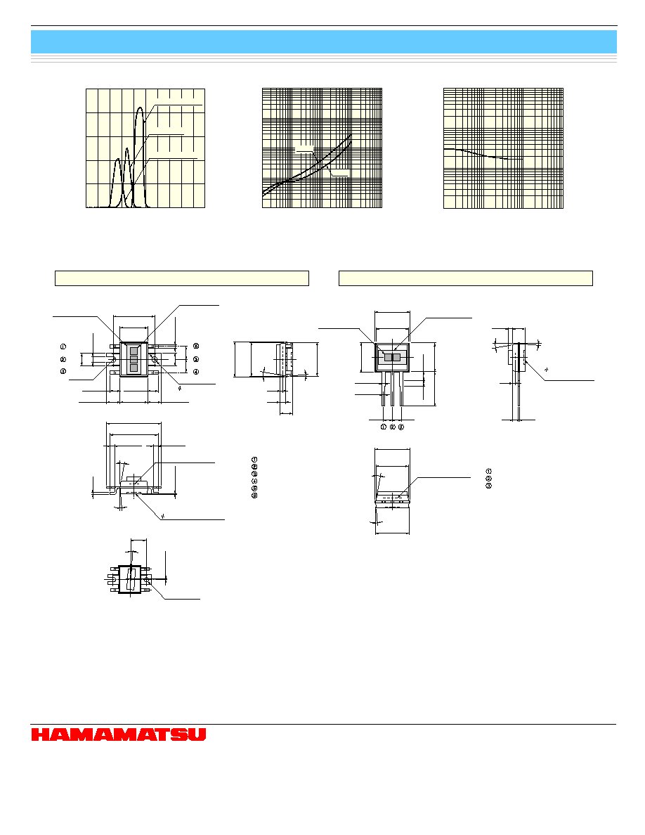
I Spectral response
KSPDB0214EA
I Dark current vs. reverse voltage
KSPDB0215EA
S8751
I Dimensional outline (unit: mm)
KSPDA0152EA
S8752
KSPDA0153EA
I Terminal capacitance vs. reverse voltage
KSPDB0216EA
Tolerance unless otherwise
noted: ±0.1, ±2∞
Shaded area indicates burr.
Chip position accuracy with respect
to the package dimensions marked *
X, Y
±0.2, ±2∞
1.8
0.55
0.4
(2
◊
) 10
∞
(2
◊
) 5
∞
ANODE (Red)
CATHODE COMMON
ANODE (Blue)
5.0 MAX.
4.7 *
(3 ◊) 0.5
2.0
DEPTH 0.15 MAX.
FILTER
ACTIVE AREA
4.2 ◊ 2.0 ◊ 0.55
t
PHOTOSENSITIVE
SURFACE
5.0 MAX.
4.7 *
4.8 *
(2 ◊) 10∞
(2 ◊) 5∞
(INCLUDING BURR)
(INCLUDING BURR)
4.2 ± 0.2
(INCLUDING B
URR)
(0.8)
(1.25)
4.0 *
4.9 ± 0.25
(3 ◊) 0.4
1.27
1.27
R B
0.8
0.25