Features
Applications
P H O T O I C
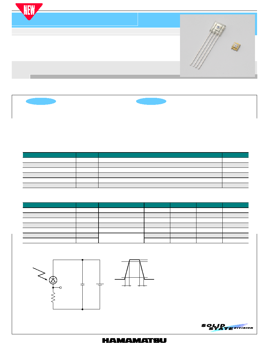
Photo IC diode
Spectral response close to visual sensitivity
S9066, S9067
PRELIMINARY DATA
Sep. 2002
S9066 and S9067 photo ICs have spectral response close to human visual sensitivity. Two active areas are made on a single chip. One is for
detecting light in the visible to near infrared range and the other is only sensitive to near infrared light and used for output signal correction. This
measures light only within the visible range by finding the difference between the two output signals in the internal current amplifier circuit.
l Spectral response close to human visual sensitivity
is attained without using visual compensation filter.
l Operation just as easy to use as a photodiode
l Large output current equivalent to phototransistors
l Excellent linearity
l Energy-saving sensor for TVs, etc.
l Light dimmers for liquid crystal panels
l Various types of light level measurement
1
I Absolute maximum ratings (Ta=25 įC)
Parameter
Symbol
Value
Unit
Reverse voltage
V
R
-0.5 to 16
V
Photocurrent
I
L
10
mA
Forward current
I
F
10
mA
Power dissipation *
P
250
mW
Operating temperature
Topr
-30 to +80
įC
Storage temperature
Tstg
-40 to +85
įC
*1: Derate power dissipation at a rate of -3.3 mW/įC above Ta=25 įC
I Electrical and optical characteristics (Ta=25 įC)
Parameter
Symbol
Condition
Min.
Typ.
Max.
Unit
Spectral response range
l
-
300 to 820
-
nm
Peak sensitivity wavelength
lp
-
600
-
nm
Operating reverse voltage
V
R
3
-
12
V
Dark current
I
D
V
R
=5 V
-
1.0
50
nA
Photocurrent
I
L
V
R
=5 V, 2856 K, 100 lx
-
0.72
-
mA
Rise time *
tr
-
6.0
-
ms
Fall time *
tf
10 to 90 %, V
R
=5 V
R
L
=10 kW, l=560 nm
-
2.5
-
ms
*2: Rise/fall time measurement method
PULSED LIGHT
FROM LED
(
l=560 nm)
V
O
LOAD
RESISTANCE R
L
7.5 V
90 %
2.5 V
10 %
V
O
tr
tf
0.1 ĶF
KPICC0041EA

HAMAMATSU PHOTONICS K.K., Solid State Division
1126-1 Ichino-cho, Hamamatsu City, 435-8558 Japan, Telephone: (81) 053-434-3311, Fax: (81) 053-434-5184, http://www.hamamatsu.com
U.S.A.: Hamamatsu Corporation: 360 Foothill Road, P.O.Box 6910, Bridgewater, N.J. 08807-0910, U.S.A., Telephone: (1) 908-231-0960, Fax: (1) 908-231-1218
Germany: Hamamatsu Photonics Deutschland GmbH: Arzbergerstr. 10, D-82211 Herrsching am Ammersee, Germany, Telephone: (49) 08152-3750, Fax: (49) 08152-2658
France: Hamamatsu Photonics France S.A.R.L.: 8, Rue du Saule Trapu, Parc du Moulin de Massy, 91882 Massy Cedex, France, Telephone: 33-(1) 69 53 71 00, Fax: 33-(1) 69 53 71 10
United Kingdom: Hamamatsu Photonics UK Limited: 2 Howard Court, 10 Tewin Road, Welwyn Garden City, Hertfordshire AL7 1BW, United Kingdom, Telephone: (44) 1707-294888, Fax: (44) 1707-325777
North Europe: Hamamatsu Photonics Norden AB: Smidesvšgen 12, SE-171 41 Solna, Sweden, Telephone: (46) 8-509-031-00, Fax: (46) 8-509-031-01
Italy: Hamamatsu Photonics Italia S.R.L.: Strada della Moia, 1/E, 20020 Arese, (Milano), Italy, Telephone: (39) 02-935-81-733, Fax: (39) 02-935-81-741
Information furnished by HAMAMATSU is believed to be reliable. However, no responsibility is assumed for possible inaccuracies or omissions.
Specifications are subject to change without notice. No patent rights are granted to any of the circuits described herein. ©2002 Hamamatsu Photonics K.K.
Cat. No. KPIC1050E03
Dec. 2002 DN
Photo IC diode
S9066, S9067
2
CATHODE
ANODE
0.4
3.2 Ī 0.2
0.4
2.3 Ī 0.2
2.2 Ī 0.2
1.4 Ī 0.1
2.7 Ī 0.2
(4 ◊) 0.5
CENTER OF ACTIVE AREA
ACTIVE AREA 0.52 ◊ 0.64
2.0 Ī 0.1
0.25 Ī 0.15
0.6
1.1 Ī 0.1
Tolerance unless otherwise
noted: Ī0.2
Active area position accuracy: X, Y
£Ī0.3
Electrodes
KPICB0075EA
I Dimensional outlines (unit: mm)
I Spectral response
0.1
0.2
0.3
0.4
0.5
0.7
0.9
0.6
0.8
1.0
0
200
400
600
800
WAVELENGTH (nm)
1000
1200
RELATIVE SENSITIVITY
(Typ. Ta=25 įC, V
R
=5 V)
S9066
S9067
CONVENTIONAL
TYPE
KPICB0076EA
I Dark current vs. ambient
temprature
KPICB0077EA
I Rise/fall time vs. load resistance
10 pA
1 nA
100 nA
10 ĶA
1 pA
100 pA
10 nA
1 ĶA
100 fA
-25
0
50
25
75
AMBIENT TEMPERATURE (įC)
100
DARK CURRENT
(Typ. V
R
=5 V)
0.1
1
10
100
0.01
100
10 k
1 k
100 k
LOAD RESISTANCE (
)
1 M
RISE/FALL TIME (ms)
(Typ. Ta=25 įC, V
R
=5 V,
=560 nm, Vo=2.5 V)
tr
tf
I Operating circuit example
KPICC0087EA
PHOTODIODE
FOR SIGNAL OFFSET
CATHODE
ANODE
C
L
R
L
Vout
REVERSE BIAS
POWER SUPPLY
THE DRAWING SURROUNDED
BY THE DOTTED LINE SHOWS
A SCHEMATIC DIAGRAM OF
THE PHOTO IC.
CURRENT
AMP
PHOTODIODE
FOR SIGNAL DETECTION
S9066
S9067
5.2 Ī 0.3
(INCLUDIG BURR)
CENTER OF ACTIVE AREA
ACTIVE AREA 0.64 ◊ 0.52
5.2 Ī 0.3
(INCLUDIG BURR)
(SPECIFIED AT THE LEAD ROOT)
PHOTOSENSITIVE
SURFACE
ANODE
(ANODE)
NC
CATHODE
(2 ◊) 1.0
(DEPTH 0.15)
2.5 Ī 0.2
5.0
2.05 Ī 0.2
5.0
16.5 Ī 1.0
(0.8)
(1.0)
1.27 1.27 1.27
10į
5į
10į
5į
0.75 Ī 0.15
10
į
5
į
10
į
5
į
0.25
+0.15
-0.1
(4 ◊) 0.55
(2 ◊) 0.45
1.0
2.0
2.0 (DEPTH 0.15)
Tolerance unless otherwise
noted: Ī0.1, Ī2į
Shaded area indicates burr.
Values in parentheses indicate
reference value.
Pin be connected to
Pin on the PC board.
KPICA0050EC
KPICA0051EB
The photodiode must be reverse-
biased so that a positive potential
is applied to the cathode.
To eliminate high-frequency
components, we recommend
placing a load capacitance C
L
in
parallel with load resistance R
L
as
a low-pass filter.
Cut-off frequency fc =
2
C
L
R
L
1
.
.