HANBit HMD1M32M2EG
URL:www.hbe.co.kr
- 1 -
HANBiT Electronics Co., Ltd
.
REV. 1.0 (August. 2002)
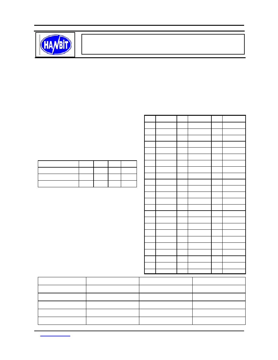
PIN ASSIGNMENT
DESCRIPTION
The HMD1M32M2EG is an 1M x 32 bits Dynamic RAM MODULE which is assembled 2 pieces of 1M x 16bit DRAMs in
42 pin SOJ package on single sides the printed circuit board with decoupling capacitors. The HMD1M32M2EG is
optimized for application to the systems, which are required high density and large capacity such as main memory of the
computers and an image memory systems, and to the others, which are, requested compact size.
The HMD1M32M2G provides common data and outputs.
Features
w
Part Indentification
-
HMD1M32M2EG
�
Gold plate Lead
w
72 pins Single In-Line Package
w
EDO Mode Capability
w
Single +5V
�
0.5V power supply
w
Fast Access Time & Cycle Time
TRAC tCAC
tRC
tHPC
HMD1M32M2EG-45
45
13
69
16
HMD1M32M2EG-50
50
15
84
20
HMD1M32M2EG-60
60
17
104
25
w
Low Power
Active: 1,870/1,650/1,430 mW(MAX)
Standby: 11mW(CMOS level : MAX)
w
/RAS Only Refresh, /CAS before /RAS Refresh,
Hidden Refresh Capability
w
All inputs and outputs TTL Compatible
w
1,024 Refresh Cycles/16ms
PIN DESCRIPTION
Pin
FUNCTION
PIN
FUNCTION
A0
�
A9
Address Inputs
PD1
�
PD4
Presence Detect
DQ0
�
DQ31
Data Input/Output
Vcc
Power (+5V)
/RAS0, /RAS2
Row Address Strobe
Vss
Ground
/CAS0 - /CAS3
Column Address Strobe
NC
No Connection
/WE
Read/Write Enable
-
-
PIN SYMBOL PIN
SYMBOL
PIN
SYMBOL
1
Vss
25
DQ22
49
DQ8
2
DQ0
26
DQ7
50
DQ24
3
DQ16
27
DQ23
51
DQ9
4
DQ1
28
A7
52
DQ25
5
DQ17
29
NC
53
DQ10
6
DQ2
30
Vcc
54
DQ26
7
DQ18
31
A8
55
DQ11
8
DQ3
32
A9
56
DQ27
9
DQ19
33
NC
57
DQ12
10
Vcc
34
/RAS2
58
DQ28
11
NC
35
NC
59
Vcc
12
A0
36
NC
60
DQ29
13
A1
37
NC
61
DQ13
14
A2
38
NC
62
DQ30
15
A3
39
Vss
63
DQ14
16
A4
40
/CAS0
64
DQ31
17
A5
41
/CAS2
65
DQ15
18
A6
42
/CAS3
66
NC
19
NC
43
/CAS1
67
PD1
20
DQ4
44
/RAS0
68
PD2
21
DQ20
45
NC
69
PD3
22
DQ5
46
NC
70
PD4
23
DQ21
47
/WE
71
NC
24
DQ6
48
NC
72
Vss
4Mbyte(1Mx32) EDO Mode, 1K Refresh, 72Pin SIMM, 5V Design
Part No. HMD1M32M2EG

HANBit HMD1M32M2EG
URL:www.hbe.co.kr
- 2 -
HANBiT Electronics Co., Ltd
.
REV. 1.0 (August. 2002)
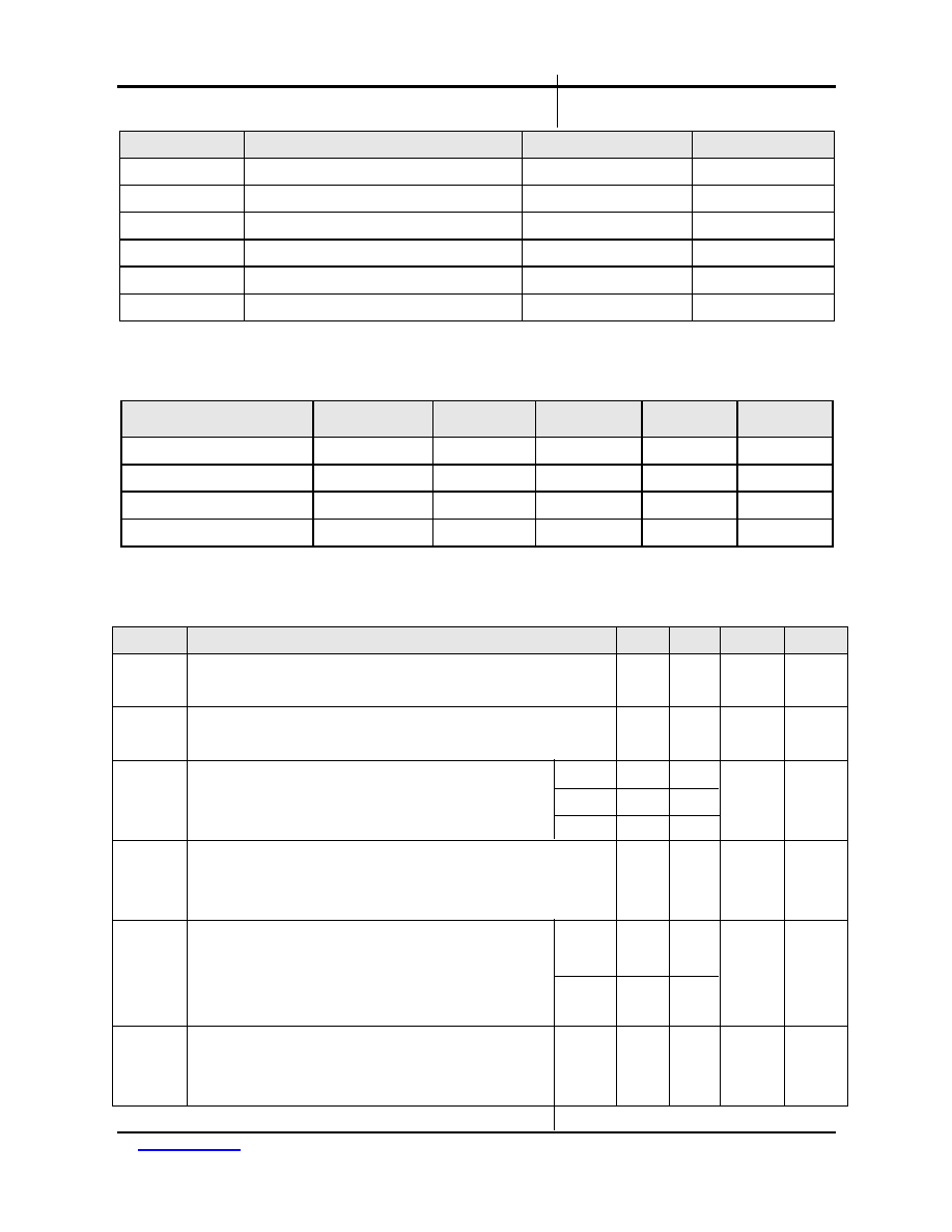
FUNCTIONAL BLOCK DIAGRAM
/RAS0
/CAS0
/CAS1
/RAS2
/CAS2
/CAS3
/WE
A0-A9
U0-U1
U0-U1 1Mx16 DRAM
U0-U1
DQ0-DQ7
DQ8-DQ15
DQ16-DQ23
DQ24-DQ31
/RAS
/LCAS
/UCAS
/OE
/WE A0-A9
U0
/RAS
/LCAS
/UCAS
/OE
/WE A0-A9
U1
Vcc
Vss
0.22uF Capacitor
C0
�
C1
DQ0
DQ1
DQ2
DQ3
DQ4
DQ5
DQ6
DQ7
DQ8
DQ9
DQ10
DQ11
DQ12
DQ13
DQ14
DQ15
DQ0
DQ1
DQ2
DQ3
DQ4
DQ5
DQ6
DQ7
DQ8
DQ9
DQ10
DQ11
DQ12
DQ13
DQ14
DQ15
HANBit HMD1M32M2EG
URL:www.hbe.co.kr
- 3 -
HANBiT Electronics Co., Ltd
.
REV. 1.0 (August. 2002)
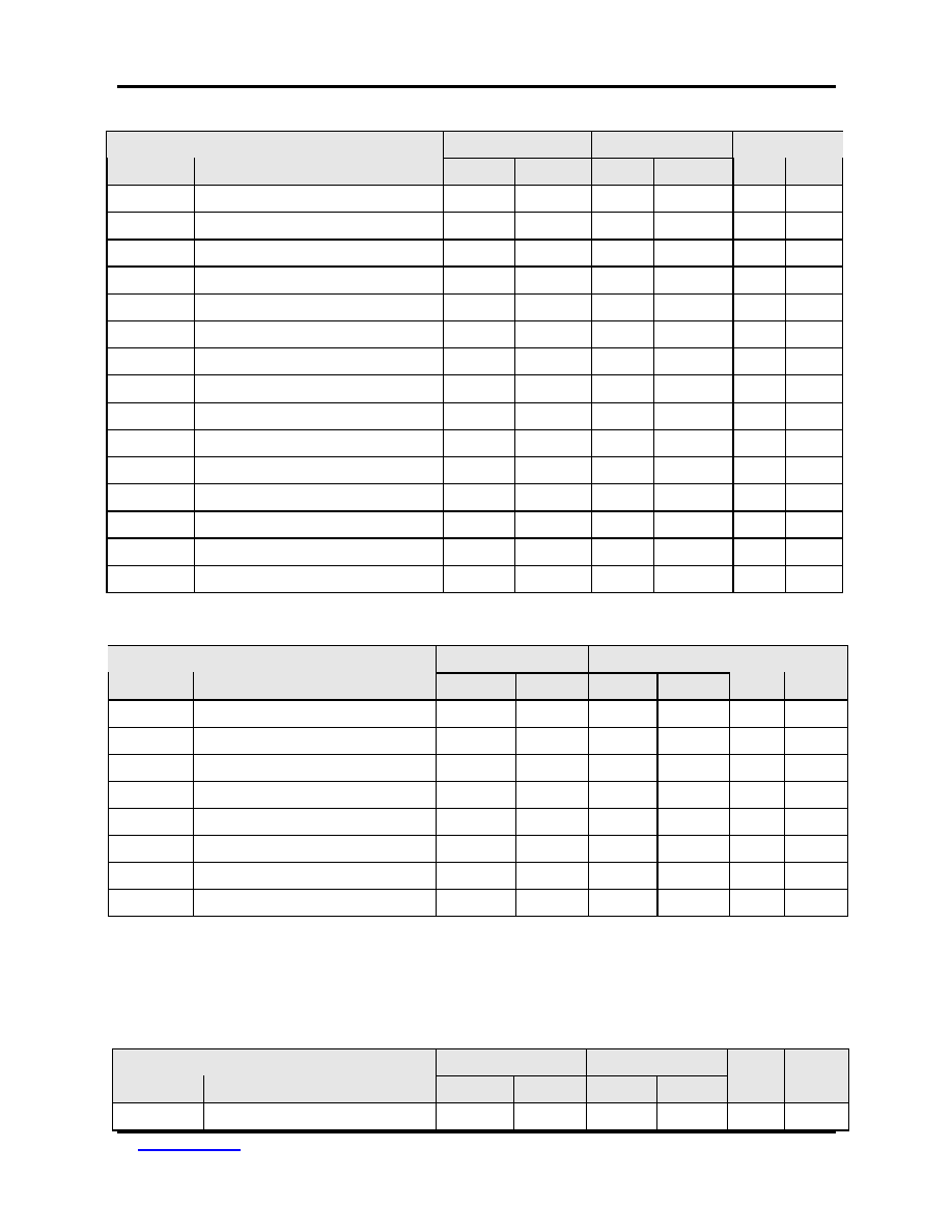
ABSOLUTE MAXIMUM RATINGS*
SYMBOL
PARAMETER
RATING
UNIT
TA
Ambient Temperature under Bias
0 ~ 70
C
TSTG
Storage Temperature (Plastic)
-55 ~ 125
C
VIN/VOUT
Voltage on any Pin Relative to Vss
-1.0 ~ 7.0
V
VCC
Power Supply Voltage
-1.0 ~ 7.0
V
IOUT
Short Circuit Output Current
50
mA
PD
Power Dissipation
2
W
*NOTE: 1. Stress greater than above absolute Maximum Ratings? May cause permanent damage to the device.
RECOMMENDED DC OPERATING CONDITIONS (TA = 0 ~ 70C)
PARAMETER
SYMBOL
MIN
TYP.
MAX
UNIT
Supply Voltage
Vcc
4.5
5.0
5.5
V
Ground
Vss
0
0
0
V
Input High Voltage
V
IH
2.4
-
Vcc+1
V
Input Low Voltage
V
IL
-1.0
-
0.8
V
*NOTE: All voltages referenced to Vcc
DC AND OPERATING CHARACTERISTICS
SYMBOL
PARAMETER
MIN
MAX
UNIT
NOTE
VOH
Output Level
Output High Level Voltage (IOUT = -5mA)
2.4
Vcc
V
VOL
Output Level
Output Low Level Voltage (IOUT = 4.2mA)
0
0.4
V
ICC1
Operating Current 60ns
Average Power Supply Operating Current 70ns
(/RAS,/CAS,Address Cycling : tRC = tRC min) -
-
-
-
340
300
-
mA
1,2
ICC2
Standby Current (TTL)
Power Supply Standby Current
(/RAS,/CAS = VIH)
-
4
mA
ICC3
/RAS Only Refresh Current 60ns
Average Power Supply Current
/RAS Only Mode 70ns
(/RAS Cycling, /CAS = VIH,: tRC = tRC min)
-
340
300
mA
2
ICC
ICC4
EDO Mode Current
Average Power Supply Current 60ns
EDO Mode
-
340
mA
1,3

HANBit HMD1M32M2EG
URL:www.hbe.co.kr
- 4 -
HANBiT Electronics Co., Ltd
.
REV. 1.0 (August. 2002)
(/RAS = VIL, /CAS, Address Cycling : tPC = tPC min) 70ns
-
300
mA
1,3
ICC5
Standby Current (CMOS)
Power Supply Standby Current
(/RAS,/CAS >= Vcc
�
0.2V)
-
2
mA
ICC6
/CAS before /RAS Refresh Current 60ns
(tRC = tRC min) 70ns
-
-
340
300
mA
ICC7
Standby Current /RAS = VIH
/CAS = VIL
DOUT = Enable
-
10
mA
1
II(L)
Input Leakage Current
Any Input (0V<=VIN<=7V)
All Other Pins Not Under Test = 0V
-10
10
uA
IO(L)
Output Leakage Current
(DOUT is Disabled, 0V<=VOUT<=7V)
-10
10
uA
Note: 1.Icc depends on output load condition when the device is selected.
Icc (max) is specified at the output open condition.
2. Address can be changed once or less while /RAS = VIL.
3. Address can be changed once or less while /CAS = VIH
CAPACITANCE
( T
A
=25
o
C, Vcc = 5V+/- 10%, f = 1Mhz )
DESCRIPTION
SYMBOL
MIN
MAX
UNITS NOTE
Input Capacitance (A0-A9)
C
I1
-
35
pF 1
Input Capacitance (/WE)
C
I2
-
34
pF 1,2
Input Capacitance (/RAS0,/RAS2)
C
I3
-
27
pF 1,2
Input Capacitance (/CAS0-/CAS3)
C
I4
-
27
pF 1,2
Input/Output Capacitance (DQ0-31)
C
DQ1
-
20
pF 1,2
Note: 1. Capacitance measured with Boonton Meter or effective capacitance measuring method.
2. /CAS = VIH to disable DOUT.
AC CHARACTERISTICS
( 0
o
C
T
A
70oC , Vcc = 5V
�
10%, See notes 1,15.)
The GMM731000CNS/SG writes data only in early write cycle (twcs>=twcs(min))
Delayed write cycle is not available because of I/O common.
HANBit HMD1M32M2EG
URL:www.hbe.co.kr
- 5 -
HANBiT Electronics Co., Ltd
.
REV. 1.0 (August. 2002)
READ, WRITE AND REFRESH CYCLE (Common Parameters)
HMD1M32M2G-6
HMD1M32M2G-7
SYMBOL
PARAMETER
MIN
MAX
MIN
MAX
UNIT
NOTE
tRC
Random Read or Write Cycle Time
110
-
130
-
ns
tPR
/RAS Precharge Time
40
-
50
-
ns
tRAS
/RAS Pulse Width
60
10K
70
10K
ns
tCAS
/CAS Pulse Width
15
10K
18
10K
ns
tASR
Row Address Setup Time
0
-
0
-
ns
tRAH
Row Address Hold Time
10
-
10
-
ns
tASC
Column Address Setup Time
0
-
0
-
ns
tcah
Column Address Hold Time
10
-
15
-
ns
9
tRCD
/RAS to /CAS Delay Time
20
45
20
52
ns
10
tRAD
/RAS to Column Address Delay Time
15
30
15
35
ns
tRSH
/RAS Hold Time
15
-
18
-
ns
tCSH
/CAS Hold Time
60
-
70
-
ns
tCRP
/CAS to /RAS Precharge Time
5
-
5
-
ns
tT
Transition Time (Rise and Fall)
3
50
3
50
ns
8
tREF
Refresh Period (1024 Cycle)
-
16
-
16
ms
Read Cycle
HMD1M32M2G-6
HMD1M32M2G-7
SYMBOL
PARAMETER
MIN
MAX
MIN
MAX
UNIT
NOTE
tRAC
Access Time from /RAS
-
60
-
70
ns
2,3
tCAC
Access Time from /CAS
-
15
-
18
ns
3,4
tAA
Access Time from Column Address
-
30
-
35
ns
3,5,14
tRCS
Read Command Setup Time
0
-
0
-
ns
tRCH
Read Command Hold Time to /CAS
0
-
0
-
ns
6
tRRH
Read Command Hold Time to /RAS
0
-
0
-
ns
6
tRAL
Column Address to /RAS Lead Time
30
-
35
-
ns
tOFF
Output Buffer Turn-off Time
-
15
-
15
ns
7
Write Cycle
HMD1M32M2G-6
HMD1M32M2G-7
SYMBOL
PARAMETER
MIN
MAX
MIN
MAX
UNIT
NOTE
twcs
Write Command Setup Time
0
-
0
-
ns
11