CAUTION: These devices are sensitive to electrostatic discharge. Users should follow proper I.C. Handling Procedures.
Copyright
©
Harris Corporation 1994
1
S E M I C O N D U C T O R
CD54AC273/3A
CD54ACT273/3A
Octal D Flip-Flop with Reset
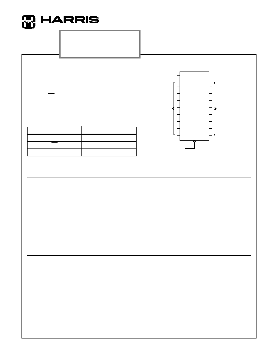
Functional Diagram
Q0
Q1
Q2
Q3
Q4
Q5
Q6
Q7
RESET MR
D0
D1
D2
D3
D4
D5
D6
D7
CLOCK
CP
DATA
INPUTS
DATA
OUTPUTS
Description
The CD54AC273/3A and CD54ACT273/3A are octal D flip-
flops with reset that utilize the Harris Advanced CMOS Logic
technology. Information at the D input is transferred to the Q
output on the positive-going edge of the clock pulse. All eight
flip-flops are controlled by a common clock (CP) and a com-
mon reset (MR). Resetting is accomplished by a low-voltage
level independent of the clock.
The CD54AC273/3A and CD54ACT273/3A are supplied in
20 lead dual-in-line ceramic packages (F suffix).
ACT INPUT LOAD TABLE
INPUT
UNIT LOAD (NOTE 1)
Dn
0.5
MR
0.57
CP
1
NOTE:
1. Unit load is
I
CC
limit specified in DC Electrical Specifications
Table, e.g., 2.4mA Max at +25
o
C.
June 1997
File Number
3904
Absolute Maximum Ratings
DC Supply Voltage, V
CC
. . . . . . . . . . . . . . . . . . . . . . . . -0.5V to +6V
DC Input Diode Current, I
IK
For V
I
< -0.5V or V
I
> V
CC
+ 0.5V
. . . . . . . . . . . . . . . . . . . . . .±
20mA
DC Output Diode Current, I
OK
For V
O
< -0.5V or V
O
> V
CC
+ 0.5V
. . . . . . . . . . . . . . . . . . . . .±
50mA
DC Output Source or Sink Current, Per Output Pin, I
O
For V
O
> -0.5V or V
O
< V
CC
+ 0.5V
. . . . . . . . . . . . . . . . . . . . .±
50mA
DC V
CC
or GND Current, I
CC
or I
GND
For Up to 4 Outputs Per Device, Add
±
25mA For Each
Additional Output
. . . . . . . . . . . . . . . . . . . . . . . . . . . . . . . . . . .±
100mA
Power Dissipation Per Package, P
D
T
A
= -55
o
C to +100
o
C (Package F) . . . . . . . . . . . . . . . . . . 500mW
T
A
= +100
o
C to +125
o
C (Package F) . . . . . . . . Derate Linearly at
8mW/
o
C to 300mW
Operating Temperature Range, T
A
Package Type F . . . . . . . . . . . . . . . . . . . . . . . . . . -55
o
C to +125
o
C
Storage Temperature, T
STG
. . . . . . . . . . . . . . . . . . -65
o
C to +150
o
C
Lead Temperature (During Soldering)
At Distance 1/16in.
±
1/32in. (1.59mm
±
0.79mm)
From Case For 10s Max . . . . . . . . . . . . . . . . . . . . . . . . . . +265
o
C
Unit Inserted Into a PC Board (Min Thickness 1/16in., 1.59mm)
With Solder Contacting Lead Tips Only. . . . . . . . . . . . . . . +300
o
C
CAUTION: Stresses above those listed in "Absolute Maximum Ratings" may cause permanent damage to the device. This is a stress only rating and operation
of the device at these or any other conditions above those indicated in the operational sections of this specification is not implied.
Recommended Operating Conditions
Supply Voltage Range, V
CC
Unless Otherwise Specified, All Voltages Referenced to GND
T
A
= Full Package Temperature Range
CD54AC Types . . . . . . . . . . . . . . . . . . . . . . . . . . . . . .1.5V to 5.5V
CD54ACT Types . . . . . . . . . . . . . . . . . . . . . . . . . . . . .4.5V to 5.5V
DC Input or Output Voltage, V
I
, V
O
. . . . . . . . . . . . . . . . . . 0V to V
CC
Operating Temperature, T
A
. . . . . . . . . . . . . . . . . . . -55
o
C to +125
o
C
Input Rise and Fall Slew Rate, dt/dv
at 1.5V to 3V (AC Types) . . . . . . . . . . . . . . . . . . . 0ns/V to 50ns/V
at 3.6V to 5.5V (AC Types) . . . . . . . . . . . . . . . . . 0ns/V to 20ns/V
at 4.5V to 5.5V (AC Types) . . . . . . . . . . . . . . . . . 0ns/V to 10ns/V
COMING SOON!
COMPLETE DATA SHEET