 | –≠–ª–µ–∫—Ç—Ä–æ–Ω–Ω—ã–π –∫–æ–º–ø–æ–Ω–µ–Ω—Ç: HC5520 | –°–∫–∞—á–∞—Ç—å:  PDF PDF  ZIP ZIP |

S E M I C O N D U C T O R
1
April 1997
HC5520
CO/PABX Polarity Reversal
Subscriber Line Interface Circuit
Features
∑ Normal and Reversed DC Feed
∑ Current Limited Loop Feed
∑ Ringing, Test-In, and Test-Out Relay Drivers
∑ Thermal Shutdown Protection with Alert Signal
∑ On-Hook Transmission
∑ Selectable Transmit and Receive Gain Setting
∑ Selectable 2-Wire Impedance Matching
∑ Zero Crossing Ring Trip Detection and Ring Relay
Release
∑ Parallel Digital Control and Status Monitoring
∑ Protection Resistors Inside Feedback Loop Allows the
Use of PTC Devices Without Impact on Longitudinal
Balance
∑ Thermal Management Features
Applications
∑ CO/PABX Line Circuits
Description
The HC5520 is a Monolithic Subscriber Line Interface Circuit
(SLIC) for Analog Subscriber Line cards in Central Office
and PABX switches.
The HC5520 provides a comprehensive set of features for
these applications including loop reversal, zero crossing
ringing relay operation, long loop drive and a mutually inde-
pendent setting of the receive and transmit gains, and the
two wire impedance synthesis. Advanced power manage-
ment features combined with a small 44 lead MQFP pack-
age allow significant board space to be freed up for
additional line circuits.
The HC5520 is fabricated in a Harris state-of-the-art Bonded
Wafer High Voltage process, providing freedom from tradi-
tional JI latch-up phenomena without the use of additional
power supply filtering components or substrate tie connec-
tions. The very low parasitics and leakages associated with
this process provide an exceptionally flat performance over
frequency and temperature.
Block Diagram
Ordering Information
PART NUMBER
TEMP.
RANGE (
o
C)
PACKAGE
PKG. NO.
HC5520CQ
0 to 70
44 Ld MQFP
Q44.10x10
HC5520CM
0 to 70
44 Ld PLCC
N44.65
TIP
TIPSEN
TEST
CONTROL
2-WIRE
INTERFACE
RING
CONTROL
AGND
BIAS
RINGSEN
RING
R
X
R
N
T
X
T
X4W
TA
TB
R
BL
R
BH
RD
C
RTD
POWER
MANAGEMENT
R
PSB
R
PST
R
PSG
RGND
BGND
V
CC
C
DC
V
EE
C
P
V
BAT
R
DC
R
PSR
BATTERY
REFERENCE
4-WIRE INTERFACE / Z
0
K
ZO
LOGIC
TAI
PDI
RCI
PRI
TBI
TSDO
SHDO
HC5520
CAUTION: These devices are sensitive to electrostatic discharge. Users should follow proper IC Handling Procedures.
Copyright
©
Harris Corporation 1997
File Number
4148.2
2
Absolute Maximum Ratings
(Note 1)
Thermal Information
V
CC
to AGND . . . . . . . . . . . . . . . . . . . . . . . . . . . . . . . . . . . . . . . . 7V
V
EE
to AGND . . . . . . . . . . . . . . . . . . . . . . . . . . . . . . . . . . . . . . . -7V
V
BAT
to BGND . . . . . . . . . . . . . . . . . . . . . . . . . . . . . . . . . . . . . . 80V
AGND to BGND . . . . . . . . . . . . . . . . . . . . . . . . . . . . . . . . . . . . .
±
3V
Digital Pins to AGND . . . . . . . . . . . . . . . . . . . . . . . . . . . -0.5V to 7V
ESD Withstand (Human Body Model) . . . . . . . . . . . . . . . . . . . 500V
Operating Conditions
Temperature Range
HC5520CQ . . . . . . . . . . . . . . . . . . . . . . . . . . . . . . . . .0
o
C to 70
o
C
HC5520CM . . . . . . . . . . . . . . . . . . . . . . . . . . . . . . . . .0
o
C to 70
o
C
Thermal Resistance (Typical, Note 1)
JA
(
o
C/W)
MQFP Package . . . . . . . . . . . . . . . . . . . . . . . . . . . .
66
PLCC Package . . . . . . . . . . . . . . . . . . . . . . . . . . . .
46
Maximum Power Dissipation
MQFP package . . . . . . . . . . . . . . . . . . . . . . . . . . . . . . . . . . . 1.21W
PLCC Package . . . . . . . . . . . . . . . . . . . . . . . . . . . . . . . . . . . . 1.74W
Maximum Junction Temperature . . . . . . . . . . . . . . . . . . . . . . . . 150
o
Maximum Storage Temperature Range . . . . . . . . . .-65
o
C to 150
o
C
Maximum Lead Temperature (Soldering 10s) . . . . . . . . . . . . . 300
o
C
(Lead tips only)
CAUTION: Stresses above those listed in "Absolute Maximum Ratings" may cause permanent damage to the device. This is a stress only rating and operation
of the device at these or any other conditions above those indicated in the operational sections of this specification is not implied.
NOTES:
1.
JA
is measured with the component mounted on an evaluation PC board in free air.
Recommended Operating Conditions
For maximum integrity, nominal operating conditions should be selected so that operation is always within the following ranges:
PARAMETER
SYMBOL
CONDITIONS
MIN
TYP
MAX
UNITS
Battery Supply
V
BAT
-42
-48
-58
V
DC
Positive Supply
V
CC
4.75
5
5.25
V
DC
Negative Supply
V
EE
-4.75
-5
-5.25
V
DC
Ringing Supply
V
RINGING
60
75
90
V
RMS
Loop Resistance
R
L
200
-
1800
Ambient Temperature
T
A
0
25
70
o
C
Die Temperature
T
D
-
-
150
o
C
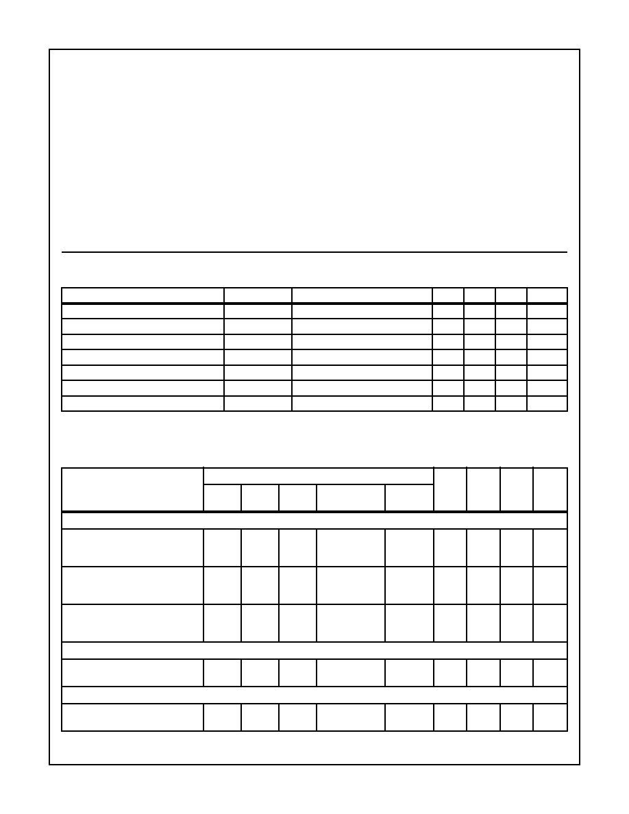
Electrical Specifications
Unless Otherwise Specified: Typical Parameters are at T
A
= 25
o
C, V
CC
= +5V, V
EE
= -5V, V
BAT
= -48V,
AGND = BGND = RGND = 0V, Min-Max Parameters are Over Power Supply and Operating Temperature Range. All Transmission Parame-
ters are Specified at 600
2-Wire Terminating Impedance with 0dB transmit and receive gain.
PARAMETER
CONDITIONS
MIN
TYP
MAX
UNITS
MODE
LOAD
V
BAT
OTHER
CONDITIONS
FREQ/
LEVEL
POWER SUPPLY CURRENTS (Figure 4)
I
CC
normal
reverse
p'down
Open
-48V
V
CC
= 5V
5.0
6.0
2.0
8.0
8.9
3.7
11.0
12.0
5.5
mA
mA
mA
I
EE
normal
reverse
p'down
Open
-48V
V
EE
= -5V
-6.0
-7.0
-3.0
-3.6
-4.9
-1.7
-2.0
-3.0
-0.7
mA
mA
mA
I
BB
normal
reverse
p'down
Open
-48V
V
CC
= 5V,
V
EE
= -5V
-7.0
-7.0
-1.0
-4.2
-4.0
-0.4
-2.0
-2.0
0.0
mA
mA
mA
THERMAL SHUTDOWN
Thermal Shutdown Temperature,
Die Temperature
normal
reverse
-48V
-
150
-
o
C
BATTERY FEED CHARACTERISTICS - 2W VOLTAGES (Figure 4)
V
TIP
normal
reverse
Open
-48V
-5.50
-46.00
-4.16
-43.60
-2.46
-42.00
V
V
HC5520

3
V
RING
normal
reverse
Open
-48V
-45.54
-6.00
-43.80
-4.26
-42.50
-2.00
V
V
V
TIP
normal
reverse
Open
-42V
-5.00
-40.00
-3.68
-38.12
-2.46
-37.00
V
V
V
RING
normal
reverse
Open
-42V
-39.54
-5.00
-38.34
-3.78
-37.00
-2.00
V
V
BATTERY FEED CHARACTERISTICS - LOOP CURRENT (Figure 5)
Normal Loop Current
normal
reverse
1800
-42V
14.5
14.5
16.5
16.3
19.0
19.0
mA
mA
Normal Loop Current
normal
reverse
1800
-48V
18.0
18.0
18.8
18.6
22.0
22.0
mA
mA
Short Circuit Loop Current Limit
normal
reverse
100
-48V
22.0
22.0
26.4
27.0
42.0
42.0
mA
mA
LOOP SUPERVISION - SWITCH HOOK DETECTION (Figure 6)
Off-Hook Detection
normal
reverse
-48V
2.4K
4.6K
9K
LOOP SUPERVISION - DIAL PULSE DISTORTION (Figure 7)
Dial Pulse Distortion
normal
100
-58V
25
o
C
-
0.1
3
%
Dial Pulse Distortion
normal
1800
-42V
25
o
C
-
0.1
3
%
LOOP SUPERVISION - RING TRIP DETECTION (Figure 8)
Ring Trip Detect
Ringing
1800
+1REN
-42V
60V
RMS
-
-
150
ms
Ring Trip Non-Detect
Ringing
3REN//
20K
-58V
90V
RMS
20K
-
-
LOOP SUPERVISION - POLARITY REVERSAL TIME (Figure 9)
Polarity Reversal Time
normal
to
reverse
1800
-42V
-
0.04
10
ms
Polarity Reversal Time
reverse
to
normal
1800
-42V
-
0.04
10
ms
LOOP SUPERVISION - DIGITAL INTERFACE
Input Low Voltage, V
IL
All Digital Inputs
-
-
0.8
V
Input High Voltage, V
IH
All Digital Inputs
2.0
-
-
V
Input Low Current, I
IL
AGND < V
IN
< V
IL
-20
-
-
µ
A
Input High Current, I
IH
V
IH
< V
IN
< V
CC
-
0
+10
µ
A
Output Low Voltage, V
OL
1 LSTTL Load
-
-
0.4
V
Output High Voltage, V
OH
1 LSTTL Load
2.4
-
-
V
Relay Driver Output Low Voltage, V
OL
V
CC
= 4.75V, Load = 35mA
-
0.4
0.8
V
Relay Driver Output High Current, I
OH
V
CC
= 5.25V
-
-
10
µ
A
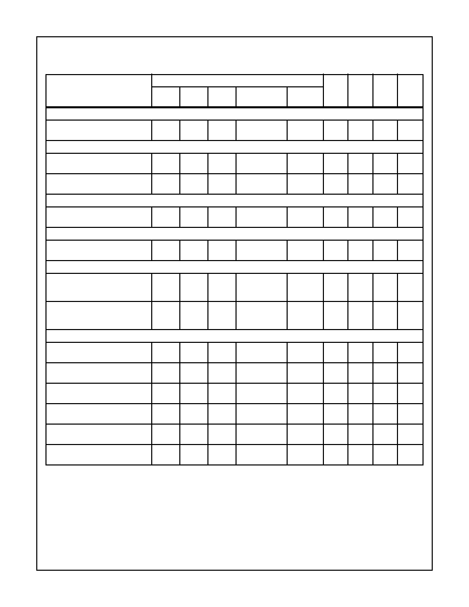
Electrical Specifications
Unless Otherwise Specified: Typical Parameters are at T
A
= 25
o
C, V
CC
= +5V, V
EE
= -5V, V
BAT
= -48V,
AGND = BGND = RGND = 0V, Min-Max Parameters are Over Power Supply and Operating Temperature Range. All Transmission Parame-
ters are Specified at 600
2-Wire Terminating Impedance with 0dB transmit and receive gain. (Continued)
PARAMETER
CONDITIONS
MIN
TYP
MAX
UNITS
MODE
LOAD
V
BAT
OTHER
CONDITIONS
FREQ/
LEVEL
HC5520

4
TRANSMISSION PARAMETERS - 4-WIRE TO 2-WIRE RECEIVE GAIN (Figure 10)
Absolute Receive Gain, ARG
normal
reverse
600
-48V
1020Hz
0dBm
-0.2
0
+0.2
dB
TRANSMISSION PARAMETERS - 4-WIRE TO 2-WIRE FREQUENCY RESPONSE (Figure 10)
Receive Frequency Response
Relative to ARG
normal
reverse
600
-48V
300 to 3.4kHz
0dBm
-0.15
0
+0.15
dB
TRANSMISSION PARAMETERS - 4-WIRE TO 2-WIRE GAIN TRACKING (Figure 10)
Receive Gain Tracking Relative to
ARG
normal
reverse
600
-48V
+3 to -40dBm0
-40 to -50dBm0
1020Hz
-0.12
-
0
0
+0.12
-
dB
dB
TRANSMISSION PARAMETERS - 4-WIRE TO 2-WIRE SIGNAL TO DISTORTION (Figure 10)
Receive Signal to Distortion and
Noise
normal
reverse
600
-48V
+3 to -40dBm0
-40 to -50dBm0
1020Hz
33
-
38
33
-
-
dB
dB
TRANSMISSION PARAMETERS - 4-WIRE TO 2-WIRE IDLE CHANNEL NOISE (Figure 10)
Idle Channel Noise
normal
reverse
600
-48V
P-Message
73
78
-
dBm0P
TRANSMISSION PARAMETERS - 2-WIRE TO 4-WIRE TRANSMIT GAIN (Figure 11)
Absolute Transmit Gain, ATG
normal
reverse
600
-48V
1020Hz
0dBm
-0.2
-0.07
+0.2
dB
TRANSMISSION PARAMETERS - 2-WIRE TO 4-WIRE FREQUENCY RESPONSE (Figure 11)
Transmit Frequency Response
Relative to ATG
normal
reverse
600
-48V
300 to 3.4kHz
0dBm
-0.2
-0.04
+0.2
dB
TRANSMISSION PARAMETERS - 2-WIRE TO 4-WIRE GAIN TRACKING (Figure 11)
Transmit Gain Tracking Relative to
ATG
normal
reverse
600
-48V
+3 to -40dBm0
-40 to -50dBm0
1020Hz
-0.12
-
0
0.02
+0.12
-
dB
dB
TRANSMISSION PARAMETERS - 2-WIRE TO 4-WIRE SIGNAL TO DISTORTION (Figure 11)
Transmit Signal to Distortion and
Noise
normal
reverse
600
-48V
+3 to -40dBm0
-40 to -50dBm0
1020Hz
33
-
38
33
-
dB
dB
TRANSMISSION PARAMETERS - 2-WIRE TO 4-WIRE IDLE CHANNEL NOISE (Figure 11)
Idle Channel Noise
normal
reverse
600
-48V
P Message
73
78
-
dB
TRANSMISSION PARAMETERS - 2-WIRE RETURN LOSS (Figure 12)
2-Wire Return Loss
normal
reverse
600
-48V
R
N
= 6490
K
ZO
= 15400
1020Hz
0dBm
30
45
-
dB
TRANSMISSION PARAMETERS - 4-WIRE TO 4-WIRE INSERTION LOSS (Figure 13)
4-Wire to 4-Wire Insertion Loss
normal
reverse
600
-48V
1020Hz
0dBm
-0.2
-0.02
+0.2
dB
TRANSMISSION PARAMETERS - TRANSHYBRID BALANCE (Figure 13)
Transhybrid Balance
normal
reverse
600
-48V
1020Hz
0dBm
30
38
-
dB
Electrical Specifications
Unless Otherwise Specified: Typical Parameters are at T
A
= 25
o
C, V
CC
= +5V, V
EE
= -5V, V
BAT
= -48V,
AGND = BGND = RGND = 0V, Min-Max Parameters are Over Power Supply and Operating Temperature Range. All Transmission Parame-
ters are Specified at 600
2-Wire Terminating Impedance with 0dB transmit and receive gain. (Continued)
PARAMETER
CONDITIONS
MIN
TYP
MAX
UNITS
MODE
LOAD
V
BAT
OTHER
CONDITIONS
FREQ/
LEVEL
HC5520
5
TRANSMISSION PARAMETERS - 4-WIRE TO 4-WIRE ABSOLUTE DELAY
Absolute Delay
normal
reverse
600
-48V
1020Hz
0dBm
1.5
µ
s
TRANSMISSION PARAMETERS - OVER LOAD LEVEL (Figures 14, 15)
Receive Over Load Level at 4W
and 2W
normal
reverse
600
-42V
1% THD
1020Hz
2.5
-
-
V
PEAK
Transmit Over Load Level at 2W
and 4W
normal
reverse
600
-42V
1% THD
1020Hz
2.15
-
-
V
PEAK
TRANSMISSION PARAMETERS - LONGITUDINAL IMPEDANCE (Figure 16)
Longitudinal Impedance per Wire
normal
reverse
-
-48V
40Hz to
100Hz
-
50
-
TRANSMISSION PARAMETERS - LONGITUDINAL CURRENT CAPABILITY (Figure 17)
Longitudinal Current Limit per Wire
normal
reverse
-
-42V
Triangle
Waveform
40Hz to
100Hz
15
-
-
mA
PEAK
TRANSMISSION PARAMETERS - LONGITUDINAL BALANCE (Figure 18)
2-Wire Longitudinal Balance
normal
reverse
368
+
368
-48V
300Hz
1020Hz
3400Hz
42
48
48
62.2
58.7
69.5
-
dB
dB
dB
4-Wire Longitudinal Balance
normal
reverse
368
+
368
-48V
300Hz
1020Hz
3400Hz
42
48
48
66.0
67.2
77.0
-
dB
dB
dB
POWER SUPPLY REJECTION RATIO (Figure 19)
PSRR V
BAT
To 4-Wire
normal
reverse
600
-48V
V
BAT
= -48V +
100mV
RMS
300Hz
30
42
-
dBC
PSRR V
BAT
To 2-Wire
normal
reverse
600
-48V
V
BAT
= -48V +
100mV
RMS
300Hz
30
42
-
dBC
PSRR V
CC
To 4-Wire
normal
reverse
600
-48V
V
CC
= 4.75V +
100mV
RMS
300Hz
20
33
-
dBC
PSRR V
CC
To 2-Wire
normal
reverse
600
-48V
V
CC
= 4.75V +
100mV
RMS
3420Hz
20
24
-
dBC
PSRR V
EE
To 4-Wire
normal
reverse
600
-48V
V
EE
= -4.75V +
100mV
RMS
2500Hz
20
30
-
dBC
PSRR V
EE
To 2-Wire
normal
reverse
600
-48V
V
EE
= -4.75V +
100mV
RMS
2500Hz
20
32
-
dBC
Electrical Specifications
Unless Otherwise Specified: Typical Parameters are at T
A
= 25
o
C, V
CC
= +5V, V
EE
= -5V, V
BAT
= -48V,
AGND = BGND = RGND = 0V, Min-Max Parameters are Over Power Supply and Operating Temperature Range. All Transmission Parame-
ters are Specified at 600
2-Wire Terminating Impedance with 0dB transmit and receive gain. (Continued)
PARAMETER
CONDITIONS
MIN
TYP
MAX
UNITS
MODE
LOAD
V
BAT
OTHER
CONDITIONS
FREQ/
LEVEL
HC5520

6
Circuit Operation and Design Information
The HC5520 is a current feed voltage sense Subscriber Line
Interface Circuit (SLIC). It provides extensive digitally con-
trolled supervisory functions, DC loop feed functions, and
user selectable 2 wire impedance matching functions.
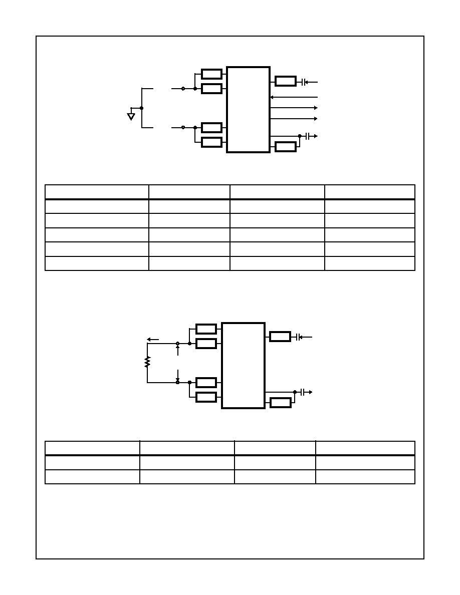
Modes of Operation
The HC5520 has seven possible modes of operation. These
modes of operation are either controlled by the digital control
inputs to the SLIC or controlled by the loop status output of
the SLIC. The modes of operation and the function of the
digital control inputs are given in Table 1.
Normal Loop Feed Mode
When PDI = 1, setting the PRI to a logic "1" places the SLIC
in the Normal Loop Feed mode. This is the normal opera-
tional mode of the SLIC. With a nominal battery supply of -
48V and an on-hook condition, the voltage at the Tip termi-
nal will be approximately 8% of the battery supply voltage. In
this case the Tip voltage is about -3.8V. Similarly, the voltage
at the Ring terminal will be approximately 92% of the battery
supply voltage or about -44.2V.
In the Normal mode the Tip voltage is more positive than
the Ring voltage; therefore, in an off-hook condition, the DC
loop current flows from Tip to Ring. The loop feeding
characteristics will be given in the battery feed section. All of
the specifications applicable to this mode of operation are
provided in the electrical specifications portion of the
HC5520 data sheet.
Reverse Loop Feed Mode
When PDI = 1, setting the PRI to a logic "0" places the SLIC
in the Reverse Loop Feed mode. In this mode, the Ring ter-
minal voltage is more positive than the Tip terminal voltage.
Thus, in an off-hook condition, the DC loop current flows
from Ring to Tip. The loop feeding characteristics in the
Reverse mode are the same as in the Normal mode. All of
the specifications applicable to this mode of operation are
provided in the electrical specifications portion of the
HC5520 data sheet.
Battery Feed
The HC5520 is designed to provide a 300
resistive feed
(150
per wire) for long loop applications. It will supply a DC
loop feed current of 18mA into an 1800
loop at the nominal
battery supply of -48V. At shorter loop lengths or higher bat-
tery supply voltages, the DC feed is current-limited to nomi-
nally 26mA in order to conserve power. For internal chip
power management purposes, external power sharing resis-
tors are used to provide some of the DC loop current. This
allows a substantial amount of the power to be dissipated off
the chip, particularly in short loop applications. A typical loop
feeding characteristic for Normal and Reverse Loop Feed
Modes of operation is shown in Figure 1.
Loop Supervision - Switch Hook Detection
The Loop Supervision circuit operates in the Normal and
Reverse Loop Feed modes. The DC loop current is moni-
tored and the off-hook condition is indicated when the loop
resistance is less than 2.4k
. When this occurs, the SHDO
output will be set to a logic low in order to signal the system
that an off-hook condition exists. If the subscriber is using a
rotary dial telephone, the system can monitor the dial pulses
through the SHDO output.
Ringing - Ring Trip Detection Mode
The ringing voltage is cadenced to a subscriber loop by
applying a logic signal to the Rci input. When a logic "0" is
received at the RCI input, the HC5520 will set the RD output
to low and thus pull current through the ring relay coil and
energize the ring relay. This causes the subscriber's tele-
phone to begin ringing. At this time the ringing current
through the ring ballast resistor is monitored to determine
whether an off-hook condition is present. Once the sub-
scriber goes off-hook, the ring trip circuit will turn off the ring
relay after the next occurrence of a zero net current flow
through the ring ballast resistor. At the same time, the SHDO
output will be set to a logic low to indicate the ring trip detec-
TABLE 1.
OPERATION
MODE
SLIC
FUNCTION
CONTROL
INPUTS
Normal
Loop Feed
Normal
Normal
PRI = High
Reverse
Loop Feed
Reverse
Normal
PRI = Low
Loop
Powerdown
P'down
Loop
power down
PDI = Low
Ringing
Ringing
Ring trip
detection only
RCI = Low
Test out
Test-out
Normal
TAI = Low
Test in
Test-in
Normal
TBI = Low
Thermal
Shut Down
TSD
Loop
Powerdown
I
LOOP
R
LOOP
600 800 1.0K 1.2K 1.4K 1.6K 1.8K 2.0K 2.2K 2.4K
10
20
30
FIGURE 1. BATTERY FEED CHARACTERISTICS
mA
HC5520

7
tion. The ring relay can not be reenergized until the system
acknowledges that a ring trip has occurred. Acknowledg-
ment is achieved by setting the RCI to a logic high.
If the subscriber goes off-hook during the silent portion of
the ringing cadence, the off-hook condition is detected in the
same manner as a switch hook detection. The SHDO output
will be set to a logic low in order to indicate that the sub-
scriber has answered the call and that ringing of the line
should cease.
Loop Power Down Mode
Under any condition when PDI is set to a logic "0", the SLIC
will power down the two wire loop. During loop power down,
the voltages at Tip and Ring are both collapsed to one-half
of the battery voltage and the outputs of the Tip and Ring
feed amplifiers are in a high impedance state. Therefore all
of the supervisory functions and transmission functions are
disabled. The HC5520 will resume normal operation once
the loop power down command is removed.
Thermal Shutdown Mode
The SLIC will power down the loop by itself once the
temperature of the SLIC die reaches 150
o
C. During this
thermal shutdown condition, both TSDO and SHDO outputs
will be set to a default logic low to indicate the condition. The
supervisory functions and transmission functions are
disabled. Once the SLIC die temperature drops 10
o
C lower
than the thermal shutdown temperature, the SLIC will
resume operation.
Test-Out and Test-In Modes
Two additional relay drivers are provided for test-out and
test-in functions. Unlike the ring relay driver circuit, these
relay drivers are operated independently of the rest of the
HC5520 circuitry. The designation of test-out and test-in is
purely arbitrary. When desired, the subscriber's loop condi-
tion can be interrogated through the test-out relay. Likewise,
through the test-in relay, the various SLIC functions and sig-
nal integrity can be examined.
Hybrid Transmission Model
Figure 2 shows a simplified model for bidirectional signal
transmission and 2-wire impedance synthesis. The term
R
SENSE
used in the equations below refers to the pair of
external 100k
sense resistors R
TPS
and R
RGS
. The
HC5520 architecture gives the user the flexibility to set the
gains and 2-wire impedance with external resistors and
resistor ratios. However, to prevent adversely affecting other
SLIC control functions, the value of R
SENSE
should always
be selected to be 100k
.
2W Impedance
The 2W impedance is the AC input impedance synthesized
by the SLIC between the Tip and Ring terminals and will be
referred to as ZO. The value of ZO is user programmable by
varying the value R
N
and Z
KZO
. R
N
is recommended to be
less than 7k
. Z
KZO
can be either a real resistance or a
complex impedance network. ZO is determined by the fol-
lowing equation:
where R
SENSE
is constrained to be 100k
.
4W to 2W Gain
The signal level voltage gain from the 4-wire analog input
(R
X
) to the 2-wire
V
TR
voltage is user programmable using
the following equation:
where R
SENSE
is constrained to be 100k
. The SLIC has a
built-in +6.02dB gain to compensate for the divider effect of
matching the load impedance, making it transparent to the
user.
2W to 4W Gain
The signal level voltage gain from the Tip and Ring terminals
(
V
TR
) to the output of the 4-wire signal amplifier (R
4W
) is
user programmable using the following equation:
Transhybrid Balance
Functionally, when a voice signal is received at V
RX
a cur-
rent which is proportional to the voice signal will pass
through the SLIC 4 wire input R
X
pin. This voice input cur-
rent will be amplified and inverted to drive the load across
the Tip and Ring. The AC voltages at Tip and Ring are fed
back to the SLIC and reproduced as the transmit signal at
the T
X
pin. This received voice signal returned from 2 wire
side of the SLIC will have the same amplitude as the
received AC signal but will be 180 degrees out of phase.
This signal needs to be eliminated from transmission to pre-
vent far end echo.
The most common way of implementing the transhybrid bal-
ance function is to use the analog voice input amplifier in the
Combo as a summing amplifier. The circuit connections are
as shown in Figure 3. Notice that the input impedance net-
works for both received signal and returned signal are bas-
cally the same, if the 62pF capacitor were not added. The
addition of the 62pF capacitor to ground is to compensate for
the phase shift of the returned signal to achieve 15dB or
more improvement in the 2k to 4kHz frequency band as
compared to the data collected from the test circuit.
Sensitive Pins
Tipsen, Ringsen Pins - These pins are very low imped-
ance virtual grounds used for providing feedback current to
the HC5520 DC, AC, and Longitudinal control loops. Para-
sitic capacitance on these pins from the PC board layout
and external components should be minimized to prevent
oscillation.
Z
O
R
SENSE
Z
KZO
∑
400
R
N
∑
-------------------------------------------------
=
A
4
2
≠
R
≠
SENSE
R
X
-----------------------------
=
A
2
4
≠
R
4W
R
SENSE
--------------------------
=
HC5520

8
K
ZO
Pin - The 2-wire impedance that is synthesized by the
HC5520 is a direct function of the network connected to this
pin (see equations). Parasitic capacitance and inductance
from the PC board layout and the external components is
magnified by the same K factor that is utilized to synthesize
the 2-wire impedance. Excessive parasitics can cause inser-
tion loss and return loss degradation, especially at higher
voice band frequencies. Good PC board layout techniques
and proper component selection can minimize these effects
to a negligible level.
R
N
Pin - This pin connects an external resistor to the input
of an internal buffer. The value of this resistor is user speci-
fied based upon the impedance desired at the 2-wire inter-
face (see equations). The value chosen must not have a
value greater than 7k
or the input voltage range of the
buffer may be exceeded during transients.
R
DC
Pin - An external resistor connected to V
CC
is required
at this pin to provide an accurate reference for the DC cur-
rents which feed the subscriber loop. PC board traces
should be made to have low resistance and should connect
directly to V
CC
.
C
DC
Pin - This pin provides a connection to the DC refer-
ence nodes that control the DC loop feed current. These
internal blocks are referenced to V
EE
and it is important that
the capacitor be referenced to V
EE
or else the PSRR perfor-
mance will be degraded.
C
P
Pin - Capacitor C
P
connects to this pin to create a low-
pass filter for the half-battery internal reference point. It is
important that this capacitor be referenced to BGND/AGND
to minimize the effect of noise injected into the subscriber
loop from the battery supply.
R
PSG
, R
PST
, R
PSR
, R
PSB
Pins - These pins are connected
to critical nodes inside the HC5519R3931 feedback control
loops. Parasitic capacitance should be minimized in order to
prevent oscillations.
RD, TB, TA Pins - The pins connect to the driver coils of the
Ring and Test relays and activate the relays by pulling down
the coil voltage to ground. The driver outputs are internally
clamped to V
CC
by diodes to prevent the inductive voltage
transient during relay turn-off from damaging the driver.
Relays attached to any voltage other than V
CC
will not func-
tion properly.
I
RX
TIP
RING
Z
L
V
TR
E
G
I
L
R
4W
V
TX
R
X
V
RX
HC5520
R
RGS
R
TPS
A = 400
I
RS
I
TS
A2
R
N
Z
KZO
I
KZO
I
RS
2x
I
RX
I
KZO
I
KZO
I
TS
I
RS
I
TS
+
-
A = 400
+
-
+
-
A1
+
-
+
-
FIGURE 2. SIMPLIFIED AC TRANSMISSION CIRCUIT
TIP
TIPSEN
RING
RINGSEN
R
TPS
R
PT
R
PR
R
RGS
R
X
TIP
RING
HC5520
T
X
600
50
50
100k
100k
R
X
100k
100k
C
VRX
0.47
µ
F
C
VTX
0.47
µ
F
V
RX
V
TX
50k
100k
100k
+
-
T
X
4
W
R
4W
VOICE INPUT
50k
0.47
µ
F
62pF
AMPLIFIER
FIGURE 3. TRANSHYBRID BALANCE CIRCUIT WITH HIGH AND LOW FREQUENCY COMPENSATION
HC5520
9
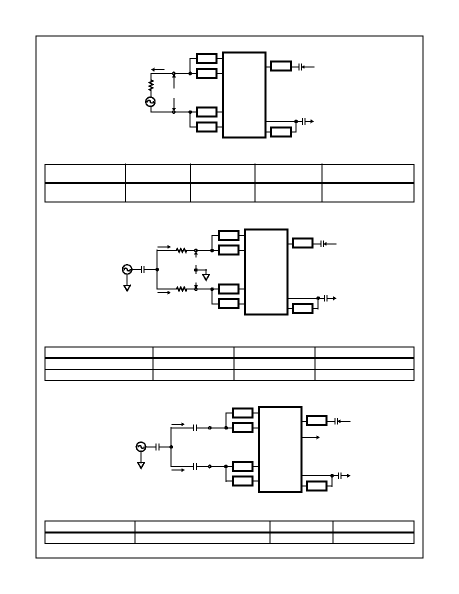
Test Information
TIP
TIPSEN
RING
RINGSEN
R
PT
R
PR
R
RGS
TIP
RING
HC5520
V
RING
V
TIP
V
CC
I
CC
V
EE
I
EE
V
BAT
I
BB
R
X
T
X
R
X
100k
R
4W
C
VRX
0.47
µ
F
C
VTX
0.47
µ
F
V
RX
V
TX
T
X4W
FIGURE 4. POWER SUPPLY CURRENT AND TIP AND RING VOLTAGE TEST CIRCUIT
PARAMETER
INPUT
MEASUREMENT
SPECIFICATIONS
Power Supply Current, I
CC
V
CC
= +4.75 ~ +5.25V
I
CC
Direct Measurement
I
CC
Power Supply Current, I
EE
V
EE
= -4.75 ~ -5.25V
I
EE
Direct Measurement
I
EE
Power Supply Current, I
BB
V
BAT
= -42 ~ -58V
I
BB
Direct Measurement
I
BB
V
TIP
V
BAT
V
TIP
Direct Measurement
V
TIP
V
RING
V
BAT
V
RING
Direct Measurement
V
RING
R
TPS
100k
50
100k
100k
50
TIP
TIPSEN
RING
RINGSEN
HC5520
V
TR
I
L
R
L
FIGURE 5. LOOP CURRENT TEST CIRCUIT
PARAMETER
INPUT
MEASUREMENT
SPECIFICATIONS
Loop Current, I
L
V
BAT
and R
L
V
TR
I
L
= V
TR
/R
L
Short Circuit Loop Current
V
BAT
= -48V and R
L
= 100
V
TR
I
L
= V
TR
/R
L
R
X
T
X
R
X
100k
R
4W
C
VRX
0.47
µ
F
C
VTX
0.47
µ
F
V
RX
V
TX
T
X4W
100k
R
PT
R
PR
R
RGS
R
TPS
100k
50
100k
50
TIP
RING
HC5520

10
>9k
2.4k
SW
R
PT
R
PR
R
RGS
R
TPS
100k
50
100k
50
TIP
TIPSEN
RING
RINGSEN
HC5520
R
X
T
X
T
X4W
R
X
100k
R
4W
C
VRX
0.472
µ
F
C
VTX
0.47
µ
F
V
RX
V
TX
100k
TIP
RING
FIGURE 6. SWITCH HOOK DETECTION TEST CIRCUIT
PARAMETER
INPUT
MEASUREMENT
SPECIFICATIONS
On Hook Condition
SW = Left
SHDO
SHDO = Hi
Off Hook Detection
SW = Right
SHDO
SHDO = Lo
SHDO
R
L
SHDO
SW
ON
SHDO
OFF
OFF-HOOK
OFF-HOOK
OFF-HOOK
OFF-HOOK
ON-HOOK
ON-HOOK
t
PERIOD
t
MAKE
t
BREAK
t
MEAS
R
X
T
X
T
X4W
FIGURE 7. DIAL PULSE DISTORTION TEST CIRCUIT AND WAVEFORMS
PARAMETER
INPUT
MEASUREMENT
SPECIFICATIONS
Percent Break
SW = On, Off, . . .
t
BREAK
and t
PERIOD
(t
BREAK
/t
PERIOD
) x 100%
Dial Pulse Distortion
SW = On, Off, . . .
t
BREAK
and t
PERIOD
and t
MEAS
Abs[(t
BREAK
- t
MEAS
)/t
PERIOD
] x 100%
SW
R
PT
R
PR
R
RGS
R
TPS
100k
50
100k
50
TIP
TIPSEN
RING
RINGSEN
HC5520
TIP
RING
R
X
100k
C
VRX
0.47
µ
F
C
VTX
0.47
µ
F
V
RX
V
TX
100k
R
4W
HC5520

11
V
RINGING
R
BL
R
BH
R
BH
R
BL
R
BAL
RD
200
1600
V
BAT
20k
C
RTD
1
µ
F
C
RTD
-5V
FIGURE 8. RING TRIP DETECTION TEST CIRCUIT
PARAMETER
INPUT
MEASUREMENT
SPECIFICATIONS
No Ring Trip Detection
SW = Up
SHDO
SHDO = Hi
Ring Trip Detection
SW = Down
SHDO
SHDO = Lo
SHDO
R
X
T
X
T
X4W
SW
R
PT
R
PR
R
RGS
R
TPS
100k
50
100k
50
TIP
TIPSEN
RING
RINGSEN
HC5520
TIP
RING
R
X
100k
C
VRX
0.47
µ
F
C
VTX
0.47
µ
F
V
RX
V
TX
100k
3 REN
1 REN
237k
1k
237k
R
4W
90%
90%
V
T
V
R
POLARITY REVERSAL COMMAND
t
REV
FIGURE 9. POLARITY REVERSAL TIME TEST CIRCUIT AND WAVEFORMS
PARAMETER
INPUT
MEASUREMENT
SPECIFICATIONS
Polarity Reversal Time
Reversal Command
t
REV
t
REV
1800
PRI
R
X
T
X
T
X4W
R
PT
R
PR
R
RGS
R
TPS
100k
50
100k
50
TIP
TIPSEN
RING
RINGSEN
HC5520
TIP
RING
RX
100k
C
VRX
0.47
µ
F
C
VTX
0.47
µ
F
V
RX
V
TX
100k
R
4W
V
T
V
R
HC5520

12
FIGURE 10. 4W TO 2W TRANSMISSION TEST CIRCUIT - NORMAL AND REVERSE MODES
PARAMETER
INPUT AT VRX
MEASUREMENT
SPECIFICATIONS AT 600
Absolute Receive Gain, AGR
0dBm0 at 1020Hz
V
TR
at 1020Hz
AGR = 20log(V
TR
/V
RX
)
Receive Frequency Response
0dBm0 at Freq
V
TR
at Freq
20log(V
TR
/V
RX
) - AGR
Receive Gain Tracking
Level at 1020Hz
V
TR
at 1020Hz
20log(V
TR
/Level) - AGR
Receive Signal to Distortion
Level at 1020Hz
V
TR
at 2nd to 5th Harmonics
20log(Level/V
TR
)
Receive Idle Channel Noise
0V
RMS
V
TR
20log(V
TR
/0.7746V
RMS
)
600
R
X
T
X
T
X4W
R
PT
R
PR
R
RGS
R
TPS
100k
50
100k
50
TIP
TIPSEN
RING
RINGSEN
HC5520
TIP
RING
R
X
100k
C
VRX
0.47
µ
F
C
VTX
0.47
µ
F
V
RX
V
TX
100k
R
4W
V
TR
600
R
X
T
X
T
X4W
R
PT
R
PR
R
RGS
R
TPS
100k
50
100k
50
TIP
TIPSEN
RING
RINGSEN
HC5520
TIP
RING
R
X
100k
C
VRX
0.47
µ
F
C
VTX
0.47
µ
F
V
RX
V
TX
100k
R
4W
FIGURE 11. 2W TO 4W TRANSMISSION TEST CIRCUIT - NORMAL AND REVERSE MODES
PARAMETER
INPUT AT V
AC
MEASUREMENT
SPECIFICATIONS AT 600
Absolute Transmit Gain, AGT
2x(0dBm0) at 1020Hz
V
TX
at 1020Hz
AGT = 20log(V
TX
/0.7746V
RMS
)
Transmit Frequency Response
2x(0dBm0) at Freq
V
TX
at Freq
20log(V
TX
/0.7746V
RMS
) - AGT
Transmit Gain Tracking
2x(Level) at 1020Hz
V
TX
at 1020Hz
20log(V
TX
/Level) - AGT
Transmit Signal to Distortion
2x(Level) at 1020Hz
V
TX
at 2nd to 5th Harmonics
20log(Level/V
TX
)
Transmit Idle Channel Noise
0V
RMS
V
TX
20log(V
TX
/0.7746V
RMS
)
V
AC
HC5520

13
FIGURE 12. 2W RETURN LOSS TEST CIRCUIT - NORMAL AND REVERSE MODES
DEFINITION : 2W Return Loss = 20 log[(Z
S
+ Z
L
) / Abs(Z
S
- Z
L
)]. Where Z
S
is the source impedance and Z
L
is the load impedance.
PARAMETER
INPUT AT V
AC
MEASUREMENT
SPECIFICATIONS FOR 600
2W Return Loss
0dBm0 at Freq
V
TR
at Freq
20log[V
AC
/Abs(2xV
TR
- V
AC
)]
600
R
X
T
X
T
X4W
R
PT
R
PR
R
RGS
R
TPS
100k
50
100k
50
TIP
TIPSEN
RING
RINGSEN
HC5520
TIP
RING
R
X
100k
C
VRX
0.47
µ
F
C
VTX
0.47
µ
F
V
RX
V
TX
100k
R
4W
V
AC
Z
S
V
TR
Z
L
V
THB
FIGURE 13. 4W TO 4W INSERTION LOSS AND TRANSHYBRID BALANCE - NORMAL AND REVERSE MODES
PARAMETER
INPUT AT V
RX
MEASUREMENT
SPECIFICATIONS FOR 600
4W to 4W Insertion Loss
0dBm0 at Freq
V
TX
at Freq
20log[V
RX
/V
TX
]
Transhybrid Balance
0dBm0 at Freq
V
THB
at Freq
20log[V
RX
/V
THB
] + 20dB
600
R
X
T
X
T
X4W
R
PT
R
PR
R
RGS
R
TPS
100k
50
100k
50
TIP
TIPSEN
RING
RINGSE
N
HC5520
TIP
RING
R
X
100k
C
VRX
0.47
µ
F
C
VTX
0.47
µ
F
V
RX
V
TX
100k
R
4W
-
+
100k
100k
1M
50k
FIGURE 14. RECEIVE OVER LOAD LEVEL AT 4W AND 2W TEST CIRCUIT - NORMAL AND REVERSE MODES
INPUT AT VRX
AT 1kHz
SLIC OUTPUT
IMPEDANCE
SLIC
VOLTAGE GAIN
MEASUREMENT
SPECIFICATION
AT 600
V
RX
= 2.50V
PEAK
600
0dB
V
TR
at 2nd to 5th Harmonics
20log(V
TR
/V
RX
)
600
R
X
T
X
T
X4W
R
PT
R
PR
R
RGS
R
TPS
100k
50
100k
50
TIP
TIPSEN
RING
RINGSEN
HC5520
TIP
RING
R
X
100k
C
VRX
0.47
µ
F
C
VTX
0.47
µ
F
V
RX
V
TX
100k
R
4W
V
TR
HC5520
14
FIGURE 15. TRANSMIT OVER LOAD LEVEL AT 2W AND 4W TEST CIRCUIT - NORMAL AND REVERSE MODES
INPUT AT V
AC
AT 1kHz
SLIC OUTPUT
IMPEDANCE
SLIC TRANSMIT
GAIN
MEASUREMENT
SPECIFICATION AT 600
V
AC
= 2x(2.15V
PEAK
)
600
0dB
V
TR
and V
TX
at
2nd to 5th Harmonics
20log[V
TR
/(V
AC
/2)]
and 20log[V
TX
/(V
AC
/2)]
600
R
X
T
X
T
X4W
R
PT
R
PR
R
RGS
R
TPS
100k
50
100k
50
TIP
TIPSEN
RING
RINGSEN
HC5520
TIP
RING
R
X
100k
C
VRX
0.47
µ
F
C
VTX
0.47
µ
F
V
RX
V
TX
100k
R
4W
V
AC
V
TR
I
L
V
AC
2.16
µ
F
368
368
I
LONG
I
LONG
FIGURE 16. LONGITUDINAL IMPEDANCE TEST CIRCUIT - NORMAL AND REVERSE MODES
PARAMETER
INPUT
MEASUREMENT
SPECIFICATIONS
Longitudinal Impedance, Tip Side
V
AC
= 0dBm0 at Freq
I
LONG
(rms) and V
T
(rms)
Z
LONG
= V
T
/I
LONG
Longitudinal Impedance, Ring Side
V
AC
= 0dBm0 at Freq
I
LONG
(rms) and V
R
(rms)
Z
LONG
= V
R
/I
LONG
R
X
T
X
T
X4W
R
PT
R
PR
R
RGS
R
TPS
100k
50
100k
50
TIP
TIPSEN
RING
RINGSEN
HC5520
TIP
RING
R
X
100k
C
VRX
0.47
µ
F
C
VTX
0.47
µ
F
V
RX
V
TX
100k
R
4W
V
T
V
R
SHDO
TRIANGULAR
WAVEFORM
V
AC
2.16
µ
F
I
LONG
I
LONG
R
X
T
X
T
X4W
R
PT
R
PR
R
RGS
R
TPS
100k
50
100k
50
TIP
TIPSEN
RING
RINGSEN
HC5520
TIP
RING
R
X
100k
C
VRX
0.47
µ
F
C
VTX
0.47
µ
F
V
RX
V
TX
100k
R
4W
FIGURE 17. ON-HOOK LONGITUDINAL CURRENT LIMIT TEST CIRCUIT - NORMAL AND REVERSE MODES
PARAMETER
INPUT
MEASUREMENT
SPECIFICATIONS
Longitudinal Current Limit
V
AC
at Freq, I
LONG
= 15mA
PEAK
SHDO
SHDO = Hi
20
µ
F
20
µ
F
HC5520

15
V
AC
2.16
µ
F
368
368
I
LONG
I
LONG
R
X
T
X
T
X4W
R
PT
R
PR
R
RGS
R
TPS
100k
50
100k
50
TIP
TIPSEN
RING
RINGSEN
HC5520
TIP
RING
R
X
100k
C
VRX
0.47
µ
F
C
VTX
0.47
µ
F
V
RX
V
TX
100k
R
4W
V
R
FIGURE 18. 2W AND 4W LONGITUDINAL BALANCE TEST CIRCUIT - NORMAL AND REVERSE MODES
PARAMETER
INPUT
MEASUREMENT
SPECIFICATIONS
2W Longitudinal Balance
V
AC
= 0dBm0 at Freq
V
TR
at Freq
20log(V
AC
/V
TR
)
4W Longitudinal Balance
V
AC
= 0dBm0 at Freq
V
TX
at Freq
20log(V
AC
/V
TX
)
V
AC
V
CC
V
EE
V
BB
600
R
X
T
X
T
X4W
R
PT
R
PR
R
RGS
R
TPS
100k
50
100k
50
TIP
TIPSEN
RING
RINGSEN
HC5520
TIP
RING
R
X
100k
C
VRX
0.47
µ
F
C
VTX
0.47
µ
F
V
RX
V
TX
100k
R
4W
V
TR
FIGURE 19. OFF HOOK PSRR 4W AND 2W TEST CIRCUIT - NORMAL AND REVERSE MODES
PARAMETER
INPUT
MEASUREMENT
SPECIFICATIONS
PSRR V
BAT
to 4W
V
BAT
= -48V + V
AC
V
TX
at Freq
20log(V
AC
/V
TX
) at Freq
PSRR V
BAT
to 2W
V
BAT
= -48V + V
AC
V
TR
at Freq
20log(V
AC
/V
TR
) at Freq
PSRR V
CC
to 4W
V
CC
= +5V + V
AC
V
TX
at Freq
20log(V
AC
/V
TX
) at Freq
PSRR V
CC
to 2W
V
CC
= +5V + V
AC
V
TR
at Freq
20log(V
AC
/V
TR
) at Freq
PSRR V
EE
to 4W
V
EE
= -5V + V
AC
V
TX
at Freq
20log(V
AC
/V
TX
) at Freq
PSRR V
EE
to 2W
V
EE
= -5V + V
AC
V
TR
at Freq
20log(V
AC
/V
TR
) at Freq
HC5520

16
Pin Descriptions
MQFP
PLCC
SYMBOL
DESCRIPTION
1
7
R
X
4W receive input pin, a ground referenced current sense input.
2
8
AGND
Analog ground pin. This pin must be tied to the BGND and RGND pins.
3
9
T
X
4W transmit output pin, a ground referenced voltage source.
4
10
T
X4W
Transmit gain setting pin - connecting a resistor between T
X4W
and T
X
establishes the 2W to 4W gain.
5
11
K
ZO
2W impedance setting pin, connecting a network K(Z
L
) between K
ZO
pin and AGND will program the 2W
impedance to be Z
L
.
6
12
R
N
Resistor divider pin for ZO, in conjunction with K
ZO
it defines the 2W impedance.
7
13
R
DC
DC feed reference pin.
8
14
C
DC
DC feeding circuit low pass filter capacitor pin.
9
15
C
P
Half battery voltage reference pin.
10
16
V
EE
Negative power supply pin, V
EE
= -5V at 5%.
11
17
TIPSEN
Tip sense input pin.
12
18
BGND
Battery ground pin. This pin must be tied to the AGND and RGND pins.
13
19
R
PSG
Power sharing resistor ground side connection pin.
14
NC
No connect.
15
20
R
PST
Power sharing resistor Tip side connection pin.
16
21
TIP
Tip feed pin.
17
22
NC
No connect.
18
23
RING
Ring feed pin.
19
24
R
PSR
Power sharing resistor Ring side connection pin.
20
25
NC
No connect.
21
26
R
PSB
Power sharing resistor battery side connection pin.
22
27
V
BAT
Battery power supply pin, V
BAT
= -42V to -58V.
23
28
RINGSEN
Ring sense input pin.
24
29
R
BH
Ring trip amplifier ground side sense input pin.
25
30
R
BL
Ring trip amplifier line side sense input pin.
26
31
C
RTD
Ring trip capacitor pin.
27
32
RD
Ring relay driver pin, open collector output. Diode protected internally.
28
33
TB
Test access relay driver pin, open collector output. Diode protected internally.
29
34
TA
Test access relay driver pin, open collector output. Diode protected internally.
30
35
RGND
Relay driver ground current return pin. This pin must be tied to the AGND and BGND pins.
31
36
V
CC
Positive power supply pin, V
CC
= +5V at 5%.
32
37
NC
No connect.
33
38
NC
No connect.
34
39
NC
No connect.
40
NC
No connect.
35
41
TAI
TA Relay Driver Control Input.
36
42
TBI
TB Relay Driver Control Input.
37
43
RCI
RD Relay Driver Control Input.
38
44
PRI
Loop Feed Polarity Control Input.
39
1
PDI
Loop Feed Control Input.
40
2
NC
No connect.
41
3
NC
No connect.
42
4
TSDO
Thermal Shutdown Indicator Output.
43
5
SHDO
Off Hook Detect Indicator Output.
44
6
NC
No connect.
HC5520

17
Typical Application Circuit Diagram
NOTE: The HC5520 application circuit is configured to provide a receive gain of 0dB, a transmit gain of 0dB, and a synthesized 2W imped-
ance of 593
. Note, the value of R
TPS
, R
RGS
should always be selected to be 100k
.
TIPSEN
TIP
RING
RINGSEN
R
PSG
R
PSR
R
PST
R
PSB
R
BH
R
BL
RGND
TA
TB
RD
TAI
TBI
RCI
PDI
PRI
TSDO
SHDO
R
X
R
N
K
ZO
T
X4W
T
X
C
DC
R
DC
C
RTD
C
P
V
CC
AGND
V
EE
BGND
V
BAT
910
0.47
µ
F
0.47
µ
F
1
µ
F
1
µ
F
4.7
µ
F
+5V
+5V
TEST
ACCESS
RELAY
RING
RELAY
0.1
µ
F
V
RX
V
TX
HC5520
TO RING
GENERATOR
R
CP
R
TPS
R
RGS
R
PR
R
PT
R
N
R
KZO
C
P
-5V
C
DC
C
RTD
R
DC
-5V
-48V
0.1
µ
F
0.1
µ
F
0.1
µ
F
+5V
TIP
RING
±
5V GND
BATTERY GND
R
PST
R
PSR
R
BH
R
BL
R
BAL
CVRX
C
VTX
R
4W
R
X
EARTH GROUND
GROUND PLANE
SURGECTOR
1K
237K
237K
100K
50
100K
50
910
910
RELAY
RELAY
RELAY
2.15K
200
15.4K
6.49K
100K
100K
HC5520

18
External Component List for Application Circuit
NAME
VALUE
TOLERANCE
RATING
R
X,
R
4W,
R
TPS
, R
RGS
100k
1%
1/10W
R
N
6.49k
1%
1/10W
R
DC
2.15k
1%
1/10W
R
BH,
R
BL
237k
1%
1/10W
R
PT
, R
PR
50
5%
2.5W or PTC
R
BAL
1000
5%
1W
R
KZ0
15.4k
1%
1/10W
R
CP
200
5%
1/10W
R
PST,
R
PSR
910
5%
2W
C
VRX,
C
VTX
0.47
µ
F
20%
10V
C
DC
4.7
µ
F
10%
10V Tantalum
C
P
1
µ
F
10%
35V Tantalum
C
RTD
1
µ
F
10%
10V Tantalum
C DECOUPLING
0.1
µ
F
20%
10V except on Vb
SURGECTOR
TISP1072F3SL
Texas Instruments
PTC
TR250-120u
Raychem
HC5520

19
HC5520
D
D1
E E1
-A-
PIN 1
A2 A1
A
5
o
-16
o
5
o
-16
o
0
o
-7
o
0.40
0.016
MIN
L
0
o
MIN
PLANE
B
0.005/0.009
0.13/0.23
WITH PLATING
BASE METAL
SEATING
0.005/0.007
0.13/0.17
B1
-B-
e
0.008
0.20
A-B
S
D
S
C
M
0.10
0.004
-C-
-D-
-H-
Metric Plastic Quad Flatpack Packages (MQFP/PQFP)
Q44.10x10
(JEDEC MO-108AA-2 ISSUE A)
44 LEAD METRIC PLASTIC QUAD FLATPACK PACKAGE
SYMBOL
INCHES
MILLIMETERS
NOTES
MIN
MAX
MIN
MAX
A
-
0.093
-
2.35
-
A1
0.004
0.010
0.10
0.25
-
A2
0.077
0.083
1.95
2.10
-
B
0.012
0.018
0.30
0.45
6
B1
0.012
0.016
0.30
0.40
-
D
0.510
0.530
12.95
13.45
3
D1
0.390
0.398
9.90
10.10
4, 5
E
0.510
0.530
12.95
13.45
3
E1
0.390
0.398
9.90
10.10
4, 5
L
0.026
0.037
0.65
0.95
-
N
44
44
7
e
0.032 BSC
0.80 BSC
-
Rev. 1 1/94
NOTES:
1. Controlling dimension: MILLIMETER. Converted inch
dimensions are not necessarily exact.
2. All dimensions and tolerances per ANSI Y14.5M-1982.
3. Dimensions D and E to be determined at seating plane
.
4. Dimensions D1 and E1 to be determined at datum plane
.
5. Dimensions D1 and E1 do not include mold protrusion.
Allowable protrusion is 0.25mm (0.010 inch) per side.
6. Dimension B does not include dambar protrusion. Allowable
dambar protrusion shall be 0.08mm (0.003 inch) total.
7. "N" is the number of terminal positions.
-C-
-H-

20
All Harris Semiconductor products are manufactured, assembled and tested under ISO9000 quality systems certification.
Harris Semiconductor products are sold by description only. Harris Semiconductor reserves the right to make changes in circuit design and/or specifications at
any time without notice. Accordingly, the reader is cautioned to verify that data sheets are current before placing orders. Information furnished by Harris is
believed to be accurate and reliable. However, no responsibility is assumed by Harris or its subsidiaries for its use; nor for any infringements of patents or other
rights of third parties which may result from its use. No license is granted by implication or otherwise under any patent or patent rights of Harris or its subsidiaries.
Sales Office Headquarters
For general information regarding Harris Semiconductor and its products, call 1-800-4-HARRIS
NORTH AMERICA
Harris Semiconductor
P. O. Box 883, Mail Stop 53-210
Melbourne, FL 32902
TEL: 1-800-442-7747
(407) 729-4984
FAX: (407) 729-5321
EUROPE
Harris Semiconductor
Mercure Center
100, Rue de la Fusee
1130 Brussels, Belgium
TEL: (32) 2.724.2111
FAX: (32) 2.724.22.05
ASIA
Harris Semiconductor PTE Ltd.
No. 1 Tannery Road
Cencon 1, #09-01
Singapore 1334
TEL: (65) 748-4200
FAX: (65) 748-0400
S E M I C O N D U C T O R
HC5520
NOTES:
1. Controlling dimension: INCH. Converted millimeter dimensions
are not necessarily exact.
2. Dimensions and tolerancing per ANSI Y14.5M-1982.
3. Dimensions D1 and E1 do not include mold protrusions. Allow-
able mold protrusion is 0.010 inch (0.25mm) per side.
4. To be measured at seating plane
contact point.
5. Centerline to be determined where center leads exit plastic body.
6. "N" is the number of terminal positions.
A1
A
SEATING
PLANE
0.020 (0.51)
MIN
VIEW "A"
D2/E2
0.025 (0.64)
0.045 (1.14)
R
0.042 (1.07)
0.056 (1.42)
0.050 (1.27) TP
E
E1
0.042 (1.07)
0.048 (1.22)
PIN (1) IDENTIFIER
C
L
D1
D
0.020 (0.51) MAX
3 PLCS
0.026 (0.66)
0.032 (0.81)
0.045 (1.14)
MIN
0.013 (0.33)
0.021 (0.53)
0.025 (0.64)
MIN
VIEW "A" TYP.
0.004 (0.10)
C
-C-
D2/E2
C
L
-C-
Plastic Leaded Chip Carrier Packages (PLCC)
N44.65
(JEDEC MS-018AC ISSUE A)
44 LEAD PLASTIC LEADED CHIP CARRIER PACKAGE
SYMBOL
INCHES
MILLIMETERS
NOTES
MIN
MAX
MIN
MAX
A
0.165
0.180
4.20
4.57
-
A1
0.090
0.120
2.29
3.04
-
D
0.685
0.695
17.40
17.65
-
D1
0.650
0.656
16.51
16.66
3
D2
0.291
0.319
7.40
8.10
4, 5
E
0.685
0.695
17.40
17.65
-
E1
0.650
0.656
16.51
16.66
3
E2
0.291
0.319
7.40
8.10
4, 5
N
44
44
6
Rev. 1 3/95