 | –≠–ª–µ–∫—Ç—Ä–æ–Ω–Ω—ã–π –∫–æ–º–ø–æ–Ω–µ–Ω—Ç: HMP8112 | –°–∫–∞—á–∞—Ç—å:  PDF PDF  ZIP ZIP |

1
Semiconductor
March 1998
HMP8112
NTSC/PAL Video Decoder
Features
∑ Supports ITU-R BT.601 (CCIR601) and Square Pixel
∑ 3 Composite Analog Inputs with Sync Tip AGC, Black
Clamping and White Peak Control
∑ Patented Decoding Scheme with Improved 2-Line
Comb Filter, Y/C Separation
∑ NTSC M, N, and PAL (B, D, G, H, I, M, N, CN) Operation
∑ Composite or S-Video Input
∑ User-Selectable Color Trap and Low Pass Video
Filters
∑ User Selectable Hue, Saturation, Contrast, Sharpness,
and Brightness Controls
∑ User Selectable Data Transfer Output Modes
- 16-Bit 4:2:2 YCbCr
- 8-Bit 4:2:2 YCbCr
∑ User Selectable Clock Range from 20MHz - 30MHz
∑ I
2
C Interface
∑ VMI Compatible Video Data Bus
Applications
∑ Multimedia PCs
∑ Video Conferencing
∑ Video Editing
∑ Video Security Systems
∑ Settop Boxes (Cable, Satellite, and Telco)
∑ Digital VCRs
∑ Related Products
- NTSC/PAL Encoders: HMP8154, HMP8156,
HMP8171, HMP8173
- NTSC/PAL Decoders: HMP8115
Description
The HMP8112 is a high quality, digital video, color decoder with
internal A/D converters. The A/D function includes a 3:1 analog
input mux, Sync Tip AGC, Black clamping and two 8-bit A/D
Converters. The high quality A/D converters minimize pixel jitter
and crosstalk.
The decoder function is compatible with NTSC M, PAL B, D,
G, H, I, M, N and special combination PAL N video stan-
dards. Both composite (CVBS) and S-Video (Y/C) input for-
mats are supported. A 2 line comb filter plus a user
selectable Chrominance trap filter provide high quality Y/C
separation. Various adjustments are available to optimize
the image such as Brightness, Contrast, Saturation, Hue and
Sharpness controls. Video synchronization is achieved with
a 4xf
SC
chroma burst lock PLL for color demodulation and
line lock PLL for correct pixel alignment. A chrominance sub-
sampling 4:2:2 scheme is provided to reduce chrominance
bandwidth.
The HMP8112 is ideally suited as the analog video interface
to VCR's and camera's in any multimedia or video system.
The high quality Y/C separation, user flexibility and inte-
grated phase locked loops are ideal for use with today's pow-
erful compression processors. The HMP8112 operates from
a single 5V supply and is TTL/CMOS compatible.
Table of Contents
Page
Functional Block Diagrams . . . . . . . . . . . . . . . . . . . . . . . . 2
Functional Operation Introduction. . . . . . . . . . . . . . . . . . . 6
Internal Register Description Tables . . . . . . . . . . . . . . . . . 14
Pinout . . . . . . . . . . . . . . . . . . . . . . . . . . . . . . . . . . . . . . . . 21
Pin Descriptions . . . . . . . . . . . . . . . . . . . . . . . . . . . . . . . . 22
AC and DC Electrical Specifications . . . . . . . . . . . . . . . . . 24
Typical Performance Curves . . . . . . . . . . . . . . . . . . . . . . . 27
Applications Information . . . . . . . . . . . . . . . . . . . . . . . . . . 39
Package Dimensions . . . . . . . . . . . . . . . . . . . . . . . . . . . . 40
Ordering Information
PART NUMBER
TEMP.
RANGE (
o
C)
PACKAGE
PKG.NO.
HMP8112CN
0 to 70
80 Ld PQFP
Q80.14x20
HMP8112EVAL2
PCI Reference Design (Includes Part)
HMP8156EVAL2
Frame Grabber Evaluation Board
(Includes Part)
PQFP is also known as QFP and MQFP
CAUTION: These devices are sensitive to electrostatic discharge. Users should follow proper IC Handling Procedures.
Copyright
©
Harris Corporation 1998
File Number
4221.3
NOT RECOMMENDED FOR NEW DESIGNS
See HMP8115

2
Functional Block Diagrams
CbCr[7:0]
Y[7:0]
A
CTIVE
FIELD
D
VLD
USER
ADJUST
.
COLOR
TRAP
OUTPUT
SAMPLE
RA
TE
CONVER
TER
STD_ERR
LOCKED
INPUT
MUX
WHITE PEAK LEVEL
DIGIT
AL COMP
ARA
T
ORS
BLA
CK LEVEL
SYNC LEVEL
8-BIT
ADC
AG
C
CLAMP
AND
VID_IN0
VID_IN1
VID_IN2/Y
CLAMP_CAP
A
GC_CAP
COMP_FIL
TER
COMP_A/D_IN
+ -
CLAMP
DIGIT
AL COMP
ARA
T
O
R
8-BIT
ADC
CLAMP
CHR
OMA_IN
CR_CLAMP_CAP
GAIN_CTRL
+
-
SD
A
SCL
RESET
GAIN
CONTR
OL
LOGIC
AND
LINE
PLL
VSYNC
DETECT
MICR
OPR
OCESSOR
INTERF
A
CE AND
CONTR
OL
HSYNC
VSYNC
LOGIC
COLOR
DEMODULA
TION
Y/C
SEP
ARA
TION
INPUT
SAMPLE
RA
TE
CONVER
TER
CHR
OMA
PLL
HSYNC
DETECT
LOCK
COLOR
ADJUST
HMP8112
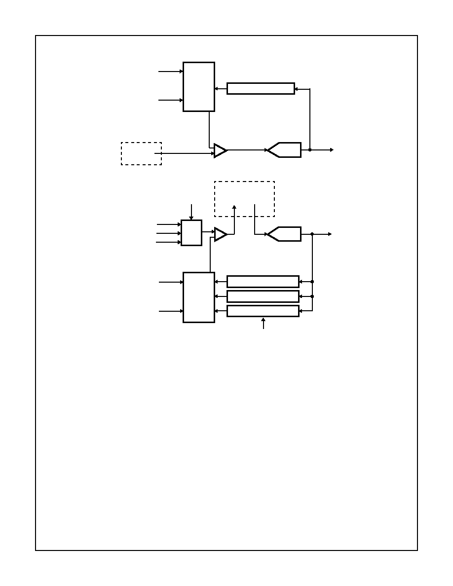
3
VIDEO INPUT
Functional Block Diagrams
(Continued)
INPUT
MUX
WHITE PEAK LEVEL
DIGITAL COMPARATORS
BLACK LEVEL
SYNC LEVEL
8-BIT
ADC
AGC
CLAMP
AND
LIN0
LIN1
LIN2
LCLAMP_CAP
LAGC_CAP
L_OUT
L_ADIN
+
-
CLAMP
DIGITAL COMPARATOR
8-BIT
ADC
CLAMP
CIN3
CCLAMP_CAP
GAIN_CTRL
+
-
GAIN
CONTROL
LOGIC
AND
LOGIC
EXTERNAL
ANTIALIASING
FILTER
EXTERNAL
ANTIALIASING
FILTER
SOURCE
SELECT
WHITE
PEAK
ENABLE
(WPE)
C
CR[7:0]
Y, CVBS
L[7:0]
HMP8112

4
VIDEO DECODER
Functional Block Diagrams
(Continued)
Y
,CVBS
C
CR[7:0]
L[7:0]
M U X
ISL
CHR
OMA
LINE
COMB
C,CVBS
DA
T
A
Y D
A
T
A
CHR
OMA TRAP
ENABLE
Y D
A
T
A
CHR
OMA
DEMODULA
T
O
R
Y D
A
T
A
C,CVBS
DA
T
A
C D
A
T
A
Y D
A
T
A
UV
AG
C
U,
V
UV
SA
TURA
TION
ADJUST
SA
TURA
TION
ADJUST
SHARPNESS
ADJUST
ST
AND
ARD
SELECT
M U X
ISL
HSYNC
DETECT
CHR
OMA
PHASE
DETECT
OR
CHR
OMA
PLL NCO
4FSC
CLOCK
CLK
(20MHz - 30MHZ)
LINE LOCKED
PLL LOOP FIL
TER
HUE
ADJUST
AG
C
ADJUST
VSYNC DETECT
INPUT
RA
TE
CONVER
TER
SAMPLE
FIL
TER
DELA
Y
TRAP
CbCr
DA
T
A
Y
DA
T
A
CLK T
O
4FSC RA
TIO
LO
W P
ASS
FIL
TER ENABLE
HSYNC
VSYNC
ST
AND
ARD ERR
OR
LOCKED
FIELD
SYNC
& CONTRAST
ADJUST
BRIGHTNESS,
STRIPPER,
OUTPUT
RA
TE
CONVER
TER
SAMPLE
LINE LOCKED
NCO
LP FIL
TER
CHR
OMA
PLL LOOP
FIL
TER
HORIZONT
AL
AND VER
TICAL
SHARPNESS
ADJUST
U
,V T
O
CbCr
COLOR
CONVER
TER
AND COLOR
KILLER
SP
A
C
E
HMP8112

5
Schematic
I
2
C CONTROL INTERFACE
OUTPUT INTERFACE
Functional Block Diagrams
(Continued)
SERIAL SHIFT
ADDRESS
POINTER
CONTROL
REGISTERS
....
....
....
....
A0
CONTROL
ADDRESS
POINTER
REGISTER
SDA
SCL
0
1
.
.
.
.
25
DATA BUS
R
E
G
I
S
T
E
R
R
E
G
I
S
T
E
R
8
8
CbCr[7:0]
Y[7:0]
Y[7:0]
CbCr[7:0]
DVLD
OEN
M
U
X
8/16 OUTPUT
SELECT
ACTIVE
FIFO
32 X 16
DEEP
JP1
JUMPER
V
CC
R10
50
C13
15pF
R2
10K
27MHz
64
63
60
58
57
56
55
54
Y7
Y6
Y5
Y4
Y3
Y2
Y1
Y0
Y7
Y6
Y5
Y4
Y3
Y2
Y1
Y0
65
66
67
71
70
ACTIVE
DVLD
FIELD
HSYNC
VSYNC
WPE
RESET
SDA
SCL
CLK
CLK
TEST
L_OUT
L_ADIN
LAGC_CAP
LCLAMP_CAP
CCLAMP_CAP
GAIN_CNTL
DEC_T
DEC_L
LIN2
LIN1
LIN0
CIN
U1
CRCB7
CRCB6
CRCB5
CRCB4
CRCB3
CRCB2
CRCB1
CRCB0
CR_CB7
CR_CB6
CR_CB5
CR_CB4
CR_CB3
CR_CB2
CR_CB1
CR_CB0
51
50
49
48
47
45
43
42
Y10. .71
Y10. .71
CR_CB10. .71
CR_CB10. .71
V
CC
V
CC
V
CC
V
CC
V
CC
V
CC
R11
10K
R12
10K
R13
10K
R14
10K
R15
10K
R16
4K
R17
4K
V
CC
RESET
27MHz
SCL
27
34
40
41
38
13
36
5
6
7
19
9
8
77
76
29
28
78
30
SDA
ACTIVE
DVLD
FIELD
VDRIVE
HDRIVE
LOW PASS FILTER
R7
680
L1
82
µ
H
R8
5.62K
C1
15pF
C4
1.0
µ
F
C5
1.0
µ
F
C3
1.0
µ
F
R5
75
R4
75
R3
75
C6
1.0
µ
F
R6
75
LUMA0
LUMA1
LUMA2
CHROMA
C2
15pF
C9
0.22
µ
F
C8
0.01
µ
F
C7
0.01
µ
F
C12
0.1
µ
F
C11
0.1
µ
F
R9
5K
AV
CC
C10
0.1
µ
F
R1
1K
R18
10
HMP8112
6
Introduction
The HMP8112 is an NTSC/PAL compatible Video Decoder
with both chroma burst and line locked digital phase locked
loops. The HMP8112 contains two 8-bit A/D converters and
an I
2
C port for programming internal registers.
Analog Video/Mux Inputs
The Luminance channel has three analog video inputs that
can be used for composite or the Y input of a S-Video signal,
and one analog input for chrominance. LIN2 is used with CIN
to interface an S-Video input. Three composite or two com-
posite and one S-Video inputs can be applied to the
HMP8112 at any one time. Control of the analog front end is
selected by bits 2 and 1 of the Video Input Control Register.
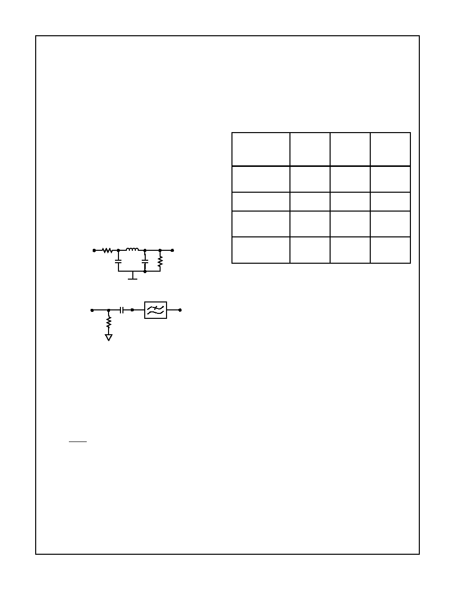
Anti-Aliasing Filter
An external anti-alias filter is required to achieve optimum
performance and prevent high frequency components from
being aliased back into the video image. For the LIN inputs a
single filter is connected to L_OUT and L_ADIN. For CIN the
anti-aliasing filter should be connected to the CIN input. A
recommended filter is shown below.
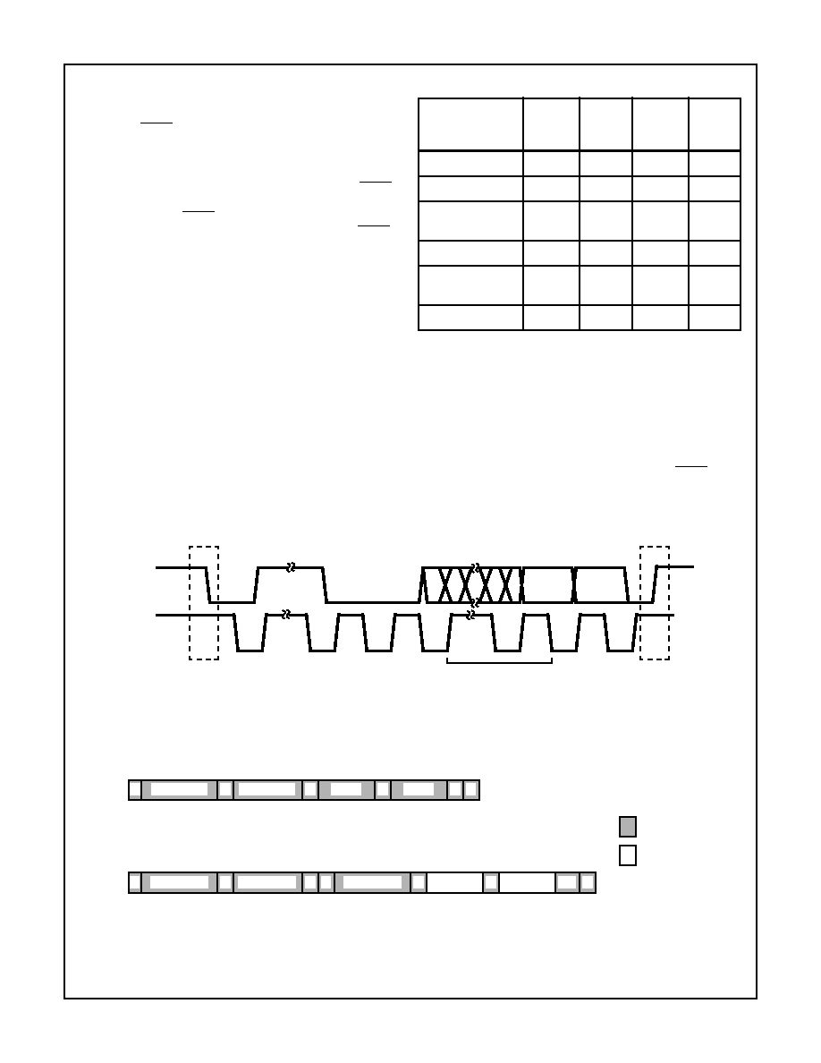
AGC And Clamp Circuit
Inputs LIN0-2 contain a sync tip AGC amplifier. During the
sync tip the value of the A/D is driven to code 0 by gaining up
the video input signal. The sync tip AGC is sampled during the
HAGC pulse time which is controlled by the HAGC Pulse Start
Time and End Time registers. The LIN0-2 inputs apply a DC
clamp reference to the back porch of the video. This is con-
trolled by the DC-RESTORE Pulse Start Time and End Time
Registers.
After a
RESET
, a change of the video standard, or a PLL
Chrominance Subcarrier Ratio Register load, HAGC and DC
RESTORE are overlapped, until LOCKED is asserted. (the
PLL has acquired a stable line lock). This is the acquisition
mode of the PLL where the decoder is trying to lock to a new
video source. Once the PLL is LOCKED, HAGC and DC
RESTORE are moved out to the default programmed values
in the user programming registers. The HAGC should be set
coincident to the incoming horizontal sync signal. The HAGC
pulse should be set to a width of 2
µ
s.
Once the PLL is locked the DC RESTORE signal is moved
out to the default programmed values in the user program-
ming registers. The DC RESTORE pulse can be pro-
grammed with the DC RESTORE Start and End time control
registers. DC RESTORE should be asserted 6.5
µ
s after the
falling edge of horizontal sync (0
HSYNC
) and held for a dura-
tion of 2
µ
s. Both HAGC and DC RESTORE are synchronous
to the output sample rate (OSR) converter and are clocked
in OSR (pixel clock) clock periods. The OSR clock rate is
dependent on the input standard used. See Table 1 for the
register values used for the different video standards.
White Peak Enable
The white peak enable input, (WPE) enables or disables the
white peak control. Enabled, (logic high) when the digital
outputs exceed code 248, the AGC will reduce the gain of
the video amplifier to prevent over-ranging the A/D. If dis-
abled, the AGC operates normally, keeping the horizontal
sync tip at code 0 and allowing the A/D's range to go to 255
at the maximum peak input.
NTSC/PAL Decoder
The NTSC/PAL decoder is designed to convert incoming
Composite or Separated (SVHS, Y/C) video into it's YCbCr
component parts. The digital phase locked loops are
designed to synchronize to the various NTSC/PAL stan-
dards. They provide a stable internal 4xf
SC
(Frequency of
the Color Sub-Carrier) video clock for color demodulation,
and a line locked clock for vertical spatial pixel alignment.
The decoder uses the CLK to run the A/D converters and the
phase locked loops. This asynchronous master clock for the
decoder eliminates the need for a unique clock source in a Mul-
timedia application. CLK can run from 20MHz to 30MHz when
using the 16-bit Synchronous Data output Mode. The user
must program the CLK to Color Sub-Carrier Ratio to match the
CLK frequency used (see Internal Phase Locked Loops discus-
sion). When using the 8-bit Burst Data Output Mode the CLK
should be a 24.5454MHz, 27MHz or 29.5MHz depending on
the output video standard chosen. The crystal oscillator must
have a
±
50ppm accuracy and a 60/40% duty cycle symmetry to
ensure proper operation. Since the video data from the external
A/D's are sampled at the CLK frequency a sample rate con-
verter is employed to convert the data from the CLK rate to the
AGND
680
82
µ
H
15pF
15pF
5.62k
L_OUT
(PIN 9)
L_ADIN
(PIN 8)
CIN
(PIN 19)
75
1.0
µ
F
CHROMA
IN
FIGURE 1. RECOMMENDED ANTI-ALIASING FILTER
LOW PASS FILTER
TABLE 1. HAGC AND DC RESTORE VALUES
VIDEO
OUTPUT
STANDARD
HAGC
START/END
VALUES
DC
RESTORE
START/END
VALUES
HSYNC
START/END
VALUES
Square Pixel
NTSC
640x480
02F8/0008
H
0028/0040
H
0020/0050
H
CCIR601 NTSC
720x480
033F/0000
H
0037/0052
H
033B/0060
H
CCIR601
PAL
720X512
033F/0000
H
0037/0052
H
033B/0060
H
Square Pixel
PAL
768X512
03A0/0018
H
0040/0054
H
0020/0070
H
HMP8112

7
internal decoding frequency of 4xf
SC
.
The input sample rate converter will interpolate between
existing CLK samples to create the chroma locked (4xf
SC
)
samples needed for the color decoder. An interpolation is
done to create the 4xf
SC
pixel and a correction factor is then
applied..
The decoder can be used with the following video sources:
Analog Composite - NTSC M, - PAL B, D, G, H, I, N
And Special Combination PAL N
Analog S - VHS (Y/C) - NTSC M, PAL B, D, G, H, I, N
And Special Combination PAL N
Color Separation, And Demodulation
To separate the chrominance modulated color information
from the baseband luminance signal, a 2 line comb filter is
employed. In NTSC signals the color information changes
phase 180
o
from one line to the next. This interleaves the
chrominance information at half line intervals throughout the
NTSC video spectrum. Therefore, NTSC has 227.5 cycles of
chrominance per NTSC line. The half of a cycle causes the
next reference burst to be 180
o
out of phase with the previ-
ous line's burst. The two line comb efficiently removes the
chrominance information from the baseband luminance sig-
nal. When decoding NTSC, the decoder maintains full lumi-
nance bandwidth horizontally throughout the chrominance
carrier frequency range. Unlike most 2 line comb filter sepa-
ration techniques, vertical bandwidth is maintained by
means of a proprietary transform technique.
For PAL systems there are 283.75 cycles of chrominance
per line. Chrominance information is spaced at quarter line
intervals with a reference phase of 135
o
. The reference
FIGURE 2A. PLL ACQUISITION MODE
FIGURE 2B. PLL LOCKED MODE
VIDEO INPUT
HAGC
DC RESTORE
OVERLAPPED CONTROL
t
PW
= 2.0
µ
s
0
HSYNC
VIDEO INPUT
HAGC
DC RESTORE
START
TIME
END
TIME
START
TIME
END
TIME
6.5
µ
s
0
HSYNC
TIME
INCOMING VIDEO SAMPLES
TIME
RESAMPLED VIDEO
4xf
SC
FIGURE 3. SAMPLE RATE CONVERSION
FREQUENCY
AMPLITUDE
f
H
/2
f
H
/2
f
H
Y
I, Q
Y
FREQUENCY
AMPLITUDE
Y
Y
I, Q
FIGURE 4. COMPOSITE NTSC INTERLEAVE SCHEME
HMP8112

8
phase alternates from line to line by 90
o
. To fully separate
the PAL chrominance and luminance signals the user select-
able filters should be enabled. The chroma notch filter built
into the luminance channel should be enabled for PAL sys-
tems to reduce cross luminance effects. The low pass filter
in the chrominance processing chain helps to reduce cross
color products.
The demodulator in the decoder decodes the color compo-
nents into U and V. The U and V components are converted
to Cb and Cr components after the decoding process.
YCbCr has a usable data range as shown in Figure 4. The
data range for Y is limited to a minimum of 16.
The decoder is compatible with all NTSC and PAL video for-
mats available throughout the world. Table 2 shows the com-
patible video standards.
Horizontal Sync Detection
Horizontal sync is detected in the Output Sample Rate con-
verter (OSR). The OSR spatially aligns the pixels in the verti-
cal direction by using the horizontal sync information
embedded in the digital video data stream. The HSYNC
sync pulse out of the decoder is a video synchronous output
pin. This signal follows the horizontal sync of an input video
source. If there is no source the HSYNC pin will continue to
run at video rates due to the Line Locked PLL free-running.
HSYNC can be moved throughout the video line using the
HSYNC Start and End time registers. This 10-bit register
allows the HSYNC to be moved in OSR clock increments
(12.27MHZ, 13.5MHz or 14.75MHz).
Vertical Sync And Field Detection
The vertical sync and field detect circuit of the decoder uses
a low time counter to detect the vertical sync sequence in
the video data stream. The low time counter accumulates
the low time encounted after the horizontal sync edge or at
the start of each line. When the low time count exceeds the
vertical
sync
detect
threshold,
VSYNC
is
asserted
immediately. VSYNC will remain asserted for a minimum of 1
line. The FIELD flag is updated at the same time as the
VSYNC line. The FIELD pin is a `0' for ODD fields and a `1'
for even fields.
In the case of lost vertical sync or excessive noise that would
prevent the detection of vertical sync, the FIELD flag will
continue to toggle. Lost vertical sync is declared if after 337
lines a vertical sync period was not detected for 3 succes-
sive lines. When this occurs the phase locked loops are ini-
tialized to the acquisition state.
The VSYNC pulse out of the decoder follows the vertical
sync detection and is typically 6.5 lines long. The VSYNC
will run at the field rate of the selected video standard
selected. For NTSC the field rate is 60Hz and for PAL the
field rate is 50Hz. This signal will continue to run even in the
event of no incoming video signal.
Internal Phase Locked Loops
The HMP8112 has two independent digital phase locked
loops on chip. A chroma phase-locked loop is implemented
to maintain chroma lock for demodulation of the color chan-
nel, and a line locked phase lock loop is implemented to
maintain vertical spatial alignment. The phase locked loops
are designed to maintain lock even in the event of VCR
headswitches and multipath noise.
The HMP8112 can use a main crystal (CLK) of 20MHz to
30MHz. The crystal is used as a reference frequency for the
internal phase locked loops. The ratio of the crystal fre-
quency to the video standard is programmed into an internal
register for the PLLs to correctly decode video.
The HMP8112 decoder contains 2 sample rate converters
and 2 phase locked loops that lock to the incoming video. The
input sample rate converter synchronizes the digitized video
from the CLK rate to a 4xf
SC
rate. The chrominance is sepa-
rated from the luminance and then demodulated. The Chroma
phase locked loop uses the CLK source as the PLL reference
frequency. To initialize the chroma PLL, the CLK to 4xf
SC
ratio
must be loaded. For example, if the CLK was 27MHz and the
video signal is NTSC (4 x 3.579545MHz = 14.318MHz) then
the ratio loaded is 0.5302895 in 16-bit precision.
FREQUENCY
AMPLITUDE
f
H
/4
f
H
Y
I, Q
Y
FREQUENCY
AMPLITUDE
Y
Y
f
H
/4
I, Q
I, Q
I, Q
FIGURE 5. COMPOSITE PAL INTERLEAVE SCHEME
Y DATA
RANGE
Cb DATA
RANGE
Cr DATA
RANGE
16
128
248
255
0
16
128
240
255
0
16
128
240
255
212
44
212
44
BLACK
WHITE
100%
BLUE
100%
BLUE
75%
YELLOW
100%
YELLOW
75%
RED
100%
RED
75%
CYAN
100%
CYAN
75%
FIGURE 6. YCbCr DATA RANGES
HMP8112

9
(4 x f
SC
)/CLK = Chroma PLL Value
(4 x 3.579545MHz) / 27MHz = 0.5302895
This value must be loaded to correctly separate and decode
the video signal. A default Chroma PLL Value is used after a
system RESET is applied. The default assumes a CLK of
27MHz and NTSC as the video standard. The default value
is 0.5302895. An ideal 4xf
SC
line should have 910 pixels for
NTSC and 1135 for PAL.
The Output Sample rate converter is locked to the horizontal
line frequency and is used to spatially align pixels in a field.
The LOCKED flag signals when the phase locked loop is
within a
±
4 pixel range of the horizontal sync edge. When
line errors exceed that range the LOCKED flag is cleared.
In cases where VCRs are used in Pause, Fast Forward or
Fast Reverse, lines are typically dropped or added by the
VCR. In a worst case scenario a VCR line tolerance will vary
by
±
8%. The standard detect logic checks the line count
against the given standard to determine an error. VCRs in
trick mode cannot cause a standard error. With an NTSC
standard VCR the number of lines in a field should not
exceed 285. Greater than 285 lines in a field is interpreted
as a PAL video source. An ideal NTSC source should have
262.5 lines per field and a PAL source should have 312.5
lines per field.
The HMP8112 can detect a STANDARD Error that signals
when the video received does not match the standard that
was programmed into the Video Input Control Register. This
TABLE 2. COMPATIBLE VIDEO INPUT STANDARDS
STANDARD
COLOR
SUBCARRIER
f
SC
NUMBER OF
FIELDS PER
SECOND
NUMBER OF
VERTICAL
LINES
LINE
FREQUENCY
NOMINAL
BANDWIDTH
BLACK
SETUP TO
BLANK
NTSC M
3.579545MHz
60Hz
525
15,734
(
±
0.0003%)
4.2MHz
7.5 IRE
PAL B, D, G, H, I
4.43361875MHz
50Hz
625
15,625
(
±
0.02%)
5.0MHz
0 IRE
PAL M
3.579545MHz
60Hz
525
15,750
(
±
0.0003%)
4.2MHz
7.5 IRE
PAL N
4.43361875MHz
50Hz
625
15,625
(
±
0.15%)
4.2MHz
7.5 IRE
Special
Combination
PAL N
3.58205625MHz
50Hz
625
15,750
(
±
0.15%)
4.2MHz
7.5 IRE
O
V
VIDEO INPUT
LOW TIME
VSYNC
FIELD
VSYNC DETECT
THRESHOLD
`EVEN' FIELD
COUNTER
6.5 LINES
FIGURE 7. VSYNC TIMING AND THE EVEN TO ODD TRANSITION
O
V
VIDEO INPUT
LOW TIME
VSYNC
FIELD
VSYNC DETECT
THRESHOLD
`ODD' FIELD
COUNTER
6.5 LINES
FIGURE 8. VSYNC TIMING AND THE ODD TO EVEN TRANSITION
HMP8112

10
flag, when asserted, tells the user that the video standard
that was expected was not found and a different standard
should be selected in the Video Input Control register. The
error flag is cleared after a RESET or after the Chroma PLL
Clock Ratio register has been loaded via the I
2
C bus. After
the flag is cleared the standard error logic verifies the video
standard. The error flag is set after 2 vertical sync periods
have passed and the line count did not match the expected
line count.
Video Adjustments
The HMP8112 allows the user to vary such video parame-
ters as Contrast, Brightness, Sharpness, Hue and Color Sat-
uration. These adjustments can be made via the I
2
C
interface. Contrast, brightness and sharpness are luminance
controls. The full dynamic range of the luminance channel
can be used by selecting the IRE setup cancellation mode.
This mode will remove the IRE setup and blanking level off-
set to take advantage of the full dynamic range of the lumi-
nance processing path. The sharpening filters allow the
enhancement of low, mid and high frequency components of
the luminance signal to compensate for low amplitude video.
Vertical sharpness is also controlled via the I
2
C interface.
Hue and Color saturation controls enhance the CbCr com-
ponents of the incoming video, all under user control.
Luminance Adjustments
The Luminance data can be adjusted in the HMP8112. The
user can adjust brightness and contrast of the Y or lumi-
nance data. The user can also set the IRE or setup subtrac-
tion value to eliminate the black pedestal offset from NTSC
signals. The Contrast adjustment range can exceed a value
of one so as to take full advantage of the 8-bit dynamic
range for Y. The user control settings executes the equation
Y
OUT
= (Y - IRE Setup + BRIGHTNESS) x CONTRAST
Brightness
The user can control the brightness of the incoming video by
programming the Brightness register. The brightness adjust-
ment will offset the Y component. The brightness register is
an 8-bit register where the bottom 7 bits are brightness con-
trol and the top bit is the IRE setup. The IRE setup for NTSC
is 70 and the setup for PAL is 63.
When the IRE bit is set (1) then the value of 70 is subtracted
from the Y data, and if the IRE bit is cleared (0) then the val-
ues of 63 is subtracted. The brightness control bits BR[6-0]
will brighten the picture as the value is increased. BR = -64
is the darkest and BR = +63 is the brightest. The default
value of the register after a RESET is 0 (80
H
).
Contrast
The contrast adjustment will allow the user to increase and
decrease the gain of the Y data. The contrast factor is an 8-bit
number (as shown below) that ranges from 0 to 1.999.
X.XXXXXXX
The default value after a RESET is 1.47 (BD
H
).
Hue or Tint Adjust
The Hue adjustment is applied to the U and the V color differ-
ence signal. The Hue adjusts the phase of the given UV data.
The Hue can be adjusted by
±
30
o
in 1/4
o
increments. This is
achieved by changing the Burst Phase Locked reference
point. Figure 10 shows the block diagram for the color adjust-
ment section. This default value for this register is 0 (00
H
).
Horizontal/Vertical Sharpness
The frequency characteristics of the video waveform can be
altered to enhance the sharpness of the picture. The Horizontal
Sharpness register acts as a 4 band equalizer where the ampli-
tude of specific frequency ranges can be enhanced or dimin-
ished. The Sharpness Control Register allows the Low (LF),
Mid (MF) and High Frequency (HF) bands of the luminance sig-
nal to be enhanced. Vertical Sharpness can be adjusted to 1 or
a factor of 0. The RESET default is a factor of 1.0
TABLE 3. USER CONTROLLED SETTINGS
USER VIDEO SETTINGS
Brightness
Contrast
Hue or Tint
Horizontal Sharpness
Vertical Sharpness
Color Saturation
IRE BLACK SETUP
+
+
-
X
BRIGHTNESS
CONTRAST
Y DATA
FROM
DECODER
Y'
8
FIGURE 9. LUMINANCE CONTROL SETTINGS PATH
(0 TO 1.999)
(NTSC = 70, PAL = 63)
(-64 TO +63)
DEMODULATED
UV DATA
UV DATA
VIDEO
DATA
HUE OFFSET
HUE
ADJUST
+
TO INPUT SAMPLE
RATE
CONVERTER
LOOP
CHROMA
PHASE LOCKED
COLOR
DECODER
CHROMA
AGC AND
USER
SETTINGS
FIGURE 10. HUE ADJUST BLOCK DIAGRAM
HMP8112

11
The 2-bit values allow 4 choices of scaling factors. The
sharpness control helps to compensate for losses in the
scaling interpolators that can reduce the amplitude of high
frequency components.
The Color Killer
(AGC Hysteresis and Loop Limits)
The color killer will disable the color difference path and set
the U and V components to zero. The automatic color killer
circuitry uses the AGC threshold to determine the maximum
and minimum gain factor limits. The loop filter determines
how much the AGC gain factor can be changed within one
line. The maximum gain factor (Max = 8) and the minimum
gain factor (Min = 0.5) will limit the range of the AGC. When
the gain factor exceeds the maximum gain factor of 8, the
gain factor is limited to 8. Once the signal has an amplitude
of 1/16th, the nominal video the color killer is enabled and
the chroma phase locked loop holds it's last phase refer-
ence. While the color killer is enabled, the U and V compo-
nents are forced to zero. Once the input video signal reaches
1/7th the optimum amplitude the color killer is disabled and
the color is returned.
The dynamic range of the AGC allows it to compensate for
video that is 1/8 to 2 times the specified nominal of 1V
P-P
.
Saturation
The color saturation component is controlled via the Color
Saturation Registers. The color saturation is applied to the
UV components after the AGC function. The saturation value
is multiplied by the UV data to increase the color intensity.
The data range is from 0 to 1.96875 where 1.96875 is the
brightest intensity. This is an 8-bit number in the form:
X.XXX XXXX
The default value after a RESET is 1.2074 (9D
H
).
I
2
C Control Interface
The HMP8112 utilizes an I
2
C control bus interface to pro-
gram the internal configuration registers. This standard
mode (up to 100 KBPS) interface consists of the bidirec-
tional Serial Data Line (SDA) and the Serial Clock Line
(SCL). The implementation on the HMP8112 is a simple
slave interface that will not respond to general calls and can-
not initiate a transfer. When the device is not active, the SDA
and SCL control pins should be pulled high through external
4k
pullup resistors.
The I
2
C clock/data timing is shown below in Figure 13. The
HMP8112 contains 29 internal registers used to program and
configure the Decoder. The I
2
C control port contains a pointer
register that auto-increments through the entire register space
and can be written. The autoincrement pointer will wrap after
the last register has been accessed (Product ID Register) and
should be set to the desired starting address each time an
access is started. For a write transfer, the I
2
C device base
address is the first part of a serial transfer. Then the internal
register pointer is loaded. Then a series of registers can be
written. If multiple registers are written, the pointer register will
autoincrement up through the register address space. A stop
cycle is used to end the transfer after the desired number of
registers are programmed.
For a read transfer, the I
2
C device address is the first part of
the serial transfer. Then the internal register pointer is
loaded. At this point another start cycle is initiated to access
the individual registers. Figure 14 shows the programming
flow for read transfer of the internal registers. Multiple regis-
ters can be read and the pointer register will autoincrement
up through the pointer register address space. On the last
data read, an acknowledge should not be issued. A stop
cycle is used to end the transfer after the desired number of
registers are read.
Product ID Register
The HMP8112 contains a product ID register that can be
used to identify the presence of a board during a Plug 'n Play
detection software algorithm. The Product ID code is 12
H
and the register is the last register in the HMP8112 (1B
H
).
Output Data Port Modes
The HMP8112 can output data in 2 formats, an 8-bit Burst
mode and a 16-bit Synchronous Pixel Transfer mode. In 16-bit
Synchronous Pixel Transfer Mode pixel data is output at the
TABLE 4. SHARPNESS GAIN FACTOR SELECTS
XF1
XF0
GAIN FACTOR
0
0
SCALED BY 1.0
0
1
SCALED BY 2.0
1
0
SCALED BY 4.0
1
1
SCALED BY 0
˜
4096
FACTOR
GAIN
MIN
I
2
C
COLOR
KILLER
LINE
COUNT
UV
DATA
AGC
ENABLE
FIGURE 11. LOOP FILTER BLOCK DIAGRAM (HYSTERESIS)
FACTOR
GAIN
MAX
AGC
GAIN
FACTOR
+5V
HMP8112
VIDEO
DECODER
+5V
SDA
SCL
+5V
40
41
4k
4k
FIGURE 12. PULLUP RESISTOR CONFIGURATION
HMP8112
12
CLK frequency and Table 5 shows the number of data points
per video line to expect for a given standard. Data is output as
4:2:2 subsampled data in a Y-Cb/Y-Cr 16-bit sequence. The
Data Valid (DVLD) flag is asserted when video data is present
on the 16-bit output port of the HMP8112 (Y[7:0], CbCr[7:0]).
The ACTIVE flag is asserted when the active video portion of
the horizontal scan line is present on the data output port. See
Figure 15 for Synchronous Pixel Transfer Mode timing. DVLD is
asserted every time the output sample rate converter has a
valid output. When DVLD and ACTIVE are used together the
visual portion of the image can be captured. When DVLD is
used alone all valid data during the Horizontal, Vertical and Ref-
erence Burst Timing are available. ACTIVE is asserted from
lines 22 through 262.5 and lines 285.5 through 525 for NTSC
(and PAL M). Active is asserted from lines 23.5 through 310
and lines 336 through 623.5 for PAL (B, D, G, H, I, N, Comb N).
The CLK can be run on a 20MHz - 30MHz clock source. Data
will be output (on average) at the Output Data Rate shown in
Table 5 for a given standard. Data is clocked out synchronous
to CLK and will come in bursts. To smooth out the data rate to
a regular rate a CLK of 2X the average output data rate can
be used. In the 16-bit pixel transfer, data is sequenced on the
CbCr[7:0] data bus, starting with Cb and then Cr.
For Burst Mode output format the Y[7:0] output bus is used
to transfer all YCbCr data in 8-bit format. The data is also
4:2:2 subsampled but will only contain the active video por-
tion of the line. The HMP8112 uses an internal 32 deep fifo
to handle latencies between the output sample rate and the
CLK frequency. In this mode, the data is clocked out at the
CLK rate and only clock frequencies of 24.5454MHz, 27MHz
and 29.5MHz can be used. In 8-bit data mode, the data is
sequenced on the Y[7:0] bus in Cb, Y, Cr, Y format. ACTIVE
is asserted as soon as the mode is selected. DVLD when
asserted indicates a valid active pixel is available. Pixels dur-
ing the horizontal and vertical blanking are not available.
Only the active portions of the video line are output.
TABLE 5. OUTPUT MODE STANDARDS
STANDARD
OUTPUT
DATA
RATE
ACTIVE
PIXELS/
LINE
TOTAL
PIXELS/
LINE
TOTAL
LINES/
FIELD
NTSC Square Pixel
12.27MHz
640
780
262.5
NTSC CCIR 601
13.5MHz
720
858
262.5
PAL B, D, G, H, I, N,
COMB N, CCIR601
13.5MHz
720
864
312.5
PAL M CCIR 601
13.5MHz
720
858
262.5
PAL B, D, G, H, I, N
Square Pixel
14.74MHz
768
944
312.5
PAL M Square Pixel 14.74MHz
640
780
312.5
SDA
SCL
START
CONDITION
S
1-7
ADDRESS
8
R/W
9
ACK
1-7
DATA
8
9
ACK
STOP
CONDITION
P
FIGURE 13. I
2
C SERIAL TIMING FLOW
S = START CYCLE
P = STOP CYCLE
A = ACKNOWLEDGE
FROM MASTER
FROM HMP8112
0x88
DATA WRITE
DATA
DATA
0x88
DATA READ
REGISTER
POINTED
TO BY
SUBADDR
REGISTER
POINTED
TO BY
SUBADDR
NA = NO ACKNOWLEDGE
0x89
1000 100 (R/W)
1000 100 (R/W)
FIGURE 14. REGISTER WRITE PROGRAMMING FLOW
S
CHIP ADDR
A
SUB ADDR
A
DATA
DATA
A
A
P
NA
A
A
CHIP ADDR
S
A
SUB ADDR
A
CHIP ADDR
S
P
HMP8112

13
Reset
The RESET pin is used to return the decoder to an initializa-
tion state. This pin should be used after a power-up to set
the part into a known state. The internal registers are
returned to their RESET state and the Serial I
2
C port is
returned to inactive state. The RESET pin is an active low
signal and should be asserted for minimum of 1 CLK cycle.
After a RESET or a software reset has occurred all output
pins are three-stated. The following pins must be pulled high
to ensure proper operation:
HSYNC
VSYNC
DVLD
ACTIVE
FIELD
A 10K or smaller pullup resistor to V
CC
is recommended.
/
CLK
Y
N
Y
0
Y
1
Y
2
t
DLY
DVLD
Y[7-0]
ACTIVE
t
DVLD
Cr
N
Cb
0
Cr
0
Cb
1
CbCr[7-0]
NOTE 1
NOTE 2
NOTES:
1. Y0 is the first active luminance pixel of a line. Cb0 and Cr0 are first active chrominance pixels in a line. Cb and Cr will alternate every cycle
due to the 4:2:2 subsampling.
2. Active is asserted for lines 22-262.5 and 285.5-525. DVLD is asserted for every valid pixel during both active and blanking regions. DVLD
is asserted during vertical and horizontal sync.
FIGURE 15A. OUTPUT TIMING 16-BIT MODE
LINES 1-21
(LINES 1-23.5)
(LINES 23.5-310)
(LINES 311-335)
(LINES 336-623.5)
LINES 263.5-284
NTSC M, N PAL M
(PAL B, D, G, H, I, N COMB N)
(PAL B, D, G, H, I, N COMB N)
NTSC M, N PAL M
FIGURE 15B. ACTIVE VIDEO REGIONS IN 16-BIT MODE
<- PIXEL 0
LINES 285-525
<- PIXEL 0
LINES 22-263.5
PIXEL 1
PIXEL 2
PIXEL 3
PIXEL N
PIXEL N-1
PIXEL N-2
PIXEL N-3
CLK
DVLDY
t
DLY
Y[7-0]
ACTIVE
t
DVLD
Cb
0
Y
0
Cr
0
Y
1
Cb
2
Y
2
Cr
2
FIGURE 16. OUTPUT TIMING 8-BIT MODE
HMP8112
14
TABLE 6. VIDEO INPUT CONTROL
DESTINATION ADDRESS = 00
H
BIT
NUMBER
FUNCTION
DESCRIPTION
RESET
STATE
7 - 6
Video Input
Standard
These bits select the video input standard.
00 = PAL B, G, H, I, N; 4.43MHz subcarrier; 50fps; 625 lines/frame;
01 = PAL M; 3.58MHz subcarrier; 60fps; 525 lines/frame;
10 = Special PAL N; 3.58MHz subcarrier; 50fps; 625 lines/frame;
11 = NTSC M; 3.58MHz subcarrier; 60fps; 525 lines/frame (default);
11
B
5
Color Trap Filter
Disable
This bit enables the color subcarrier trap filter. The filter removes the color subcarrier infor-
mation from the luminance channel. The filter should be enabled for PAL Standard systems.
0 = Enabled
1 = Disabled (default)
1
B
4
Chrominance Low
Pass Filter Disable
This bit enables the chrominance low pass filter. This filter band limits the chrominance
channel to remove luminance artifacts. This filter should be enabled for PAL Standard
systems.
0 = Enabled
1 = Disabled (default)
1
B
3
Automatic Color
Gain Control
This bit enables the color AGC function. When this bit is set the color AGC will automati-
cally adjust the chrominance channel gain, to drive the color reference burst to a nominal
±
20 IRE's. When this bit is cleared the color AGC gain factor is set to 1.0 and the color
saturation must be adjusted to obtain nominal CrCb values.
0 = Disabled
1 = Enabled (default)
1
B
2 - 1
A/D Converter
Multiplexor Selects
These bits control the A/D input select multiplexers and whether S-Video is being input as
follows: MUXSEL1,0 =
0, 0 = Select Composite Video Input #0, set decoder for Composite
1, 0 = Select Composite Video Input #1, set decoder for Composite
0, 1 = Select Composite Video Input #2, set decoder for Composite
1, 1 = Select S-Video Y and C Inputs
00
B
0
Not Used
Write Ignored, Read 0's
X
B
TABLE 7. LUMINANCE BRIGHTNESS CONTROL
DESTINATION ADDRESS = 01
H
BIT
NUMBER
FUNCTION
DESCRIPTION
RESET
STATE
7
IRE Setup
Cancellation Control
This bit enables the black setup cancelation circuit for NTSC sources. When this bit is set
a value of 73 is used to strip the sync information from the video signal. When this bit is
cleared a value of 64 is used to strip the sync information.
0 = subtract 64 from the luminance signal
1 = subtract 73 from the luminance signal
1
B
6 - 0
Luminance
Brightness Control
These bits control the brightness adjustment to the luminance channel. The brightness
adjustment value is a number that ranges from +63 to -64. This register is in the two's
complement format, where bit 6 is the sign bit.
000 0000
B
HMP8112

15
TABLE 8. LUMINANCE CONTRAST ADJUST REGISTER
DESTINATION ADDRESS = 02
H
BIT
NUMBER
FUNCTION
DESCRIPTION
RESET
STATE
7 - 0
Luminance Contrast
Adjust Factor
This register sets the contrast adjust factor. This value is multiplied by the luminance data
and allows the data to be scaled from 0 to a factor of +1.96875. This 8-bit number is a
fractional number as shown below:
2
0
2
-1
2
-2
2
-3
2
-4
2
-5
2
-6
2
-7
The contrast factor is applied after the brightness.
1011 1101
B
TABLE 9. HUE ADJUST REGISTER
DESTINATION ADDRESS = 03
H
BIT
NUMBER
FUNCTION
DESCRIPTION
RESET
STATE
7 - 0
Hue Phase Adjust
This register sets the hue phase offset adjustment. This 8-bit number is applied as a
phase offset to the CbCr data coming out of the demodulator. This 8-bit number is a in
the range of +127 to -128. The hue adjust has as range of 30
o
with each count in this
register allowing a 0.25
o
phase adjustment. This register is in two's complement format,
where bit 7 is the sign bit.
0000 0000
B
TABLE 10. LUMINANCE SHARPNESS CONTROL REGISTER
DESTINATION ADDRESS = 04
H
BIT
NUMBER
FUNCTION
DESCRIPTION
RESET
STATE
7 - 6
High Frequency
Enhancement Factor
These bits adjust the amplitude of high frequency components in the luminance video
signal. The attenuation or multiplication of the high frequency components is adjusted as
shown below:
00 = Multiply high frequency components by 1.0
01 = Multiply high frequency components by 2.0
10 = Multiply high frequency components by 4.0
11 = Zero out high frequency components.
00
B
5 - 4
Middle Frequency
Enhancement
Factor
These bits adjust the amplitude of middle frequency components in the luminance video
signal. The attenuation or multiplication of the middle frequency components is adjusted
as shown below:
00 = Multiply middle frequency components by 1.0
01 = Multiply middle frequency components by 2.0
10 = Multiply middle frequency components by 4.0
11 = Zero out middle frequency components.
00
B
3 - 2
Low Frequency
Enhancement
Factor
These bits adjust the amplitude of low frequency components in the luminance video sig-
nal. The attenuation or multiplication of the low frequency components is adjusted as
shown below:
00 = Multiply low frequency components by 1.0
01 = Multiply low frequency components by 2.0
10 = Multiply low frequency components by 4.0
11 = Zero out low frequency components.
00
B
1 - 0
Vertical High
Frequency
Enhancement
Factor
These bits adjust the amplitude of vertical high frequency components in the luminance
video signal. The attenuation or multiplication of the vertical high frequency components
is adjusted as shown below:
00 = Multiply vertical high frequency components by 1.0
01 = Reserved.
10 = Reserved.
11 = Zero out vertical high frequency components.
00
B
HMP8112
16
TABLE 11. COLOR SATURATION ADJUST FACTOR
DESTINATION ADDRESS = 05
H
BIT
NUMBER
FUNCTION
DESCRIPTION
RESET
STATE
7 - 0
Color Saturation
Adjust Factor
This register sets the color saturation adjust factor. This value is multiplied by the chromi-
nance (CbCr) data and allows the data to be scaled from 0 to a factor of +1.96875. This 8-bit
number is a fractional number as shown below:
2
0
2
-1
2
-2
2
-3
2
-4
2
-5
2
-6
2
-7
The contrast factor is applied after the brightness.
1001 1101
B
TABLE 12. PHASE LOCKED LOOP CHROMINANCE SUBCARRIER TO BUS CLOCK FREQUENCY RATIO
DESTINATION ADDRESS = 06
H
BIT
NUMBER
FUNCTION
DESCRIPTION
RESET
STATE
7 - 0
Chroma PLL Ratio
These bits are used to program the ratio of the incoming video chrominance color sub-
carrier frequency to the BUS Clock used. This number serves as the reference frequency
of the chrominance PLL and must be very accurate. This is the lower byte of the ratio and
encompasses the following range:
2
-9
2
-10
2
-11
2
-12
2
-13
2
-14
2
-15
2
-16
The default value is for a CLK frequency of 27MHz and a color subcarrier of 3.579545
MHz.
1100 0001
B
TABLE 13. PHASE LOCKED LOOP CHROMINANCE SUBCARRIER TO BUS CLOCK FREQUENCY RATIO
DESTINATION ADDRESS = 07
H
BIT
NUMBER
FUNCTION
DESCRIPTION
RESET
STATE
15 - 8
Chroma PLL Ratio
These bits are used to program the ratio of the incoming video chrominance color sub-
carrier frequency to the BUS Clock used. This number serves as the reference frequency
of the chrominance PLL and must be very accurate. This is the upper byte of the ratio
and encompasses the following range:
2
-1
2
-2
2
-3
2
-4
2
-5
2
-6
2
-7
2
-8
1000 0111
B
TABLE 14. HORIZONTAL AGC START TIME REGISTER
DESTINATION ADDRESS = 08
H
BIT
NUMBER
FUNCTION
DESCRIPTION
RESET
STATE
7 - 0
Horizontal AGC
Pulse Programmable
Start Time
This register provides a programmable delay for the HAGC pulse that control the sync
tip AGC in the A/D converters. The start time of the HAGC pulse is set from the detection
of horizontal sync in the video data. HAGC is programmable in CLK increments and has
a fixed 1 clock delay following the falling edge of horizontal sync. This is the lower byte
of the 10-bit word.
0011 1111
B
TABLE 15. HORIZONTAL AGC START TIME REGISTER
DESTINATION ADDRESS = 09
H
BIT
NUMBER
FUNCTION
DESCRIPTION
RESET
STATE
15 - 10
Not Used
Write Ignored, Read 0's.
XXXX XX
HMP8112

17
9 - 8
Horizontal AGC
Pulse Programmable
Start Time
This register provides a programmable delay for the HAGC pulse that control the sync
tip AGC in the A/D converters. The start time of the HAGC pulse is set from the detection
of horizontal sync in the video data. HAGC is programmable in CLK increments and has
a fixed 1 clock delay following the falling edge of horizontal sync. This is the upper byte
of the 10-bit word.
11
B
TABLE 16. HORIZONTAL AGC END TIME REGISTER
DESTINATION ADDRESS = 0A
H
BIT
NUMBER
FUNCTION
DESCRIPTION
RESET
STATE
7 - 0
Horizontal AGC
Pulse Programmable
End Time
This register provides a programmable delay for the HAGC pulse that control the sync
tip AGC in the A/D converters. The end time of the HAGC pulse is set from the detection
of horizontal sync in the video data. HAGC is programmable in CLK increments and has
a fixed 1 clock delay following the falling edge of horizontal sync. This is the lower byte
of the 10-bit word.
0000 0000
B
TABLE 17. HORIZONTAL AGC END TIME REGISTER
DESTINATION ADDRESS = 0B
H
BIT
NUMBER
FUNCTION
DESCRIPTION
RESET
STATE
15 - 10
Not Used
Write Ignored, Read 0's
XXXX XX
9 - 8
Horizontal AGC
Pulse Programmable
End Time
This register provides a programmable delay for the HAGC pulse that control the sync
tip AGC in the A/D converters. The end time of the HAGC pulse is set from the detection
of horizontal sync in the video data. HAGC is programmable in CLK increments and has
a fixed 1 clock delay following the falling edge of horizontal sync. This is the upper byte
of the 10-bit word.
00
B
TABLE 18. HORIZONTAL SYNC START TIME REGISTER
DESTINATION ADDRESS = 0C
H
BIT
NUMBER
FUNCTION
DESCRIPTION
RESET
STATE
7 - 0
Horizontal Drive
Programmable Start
Time
This register provides a programmable delay for the external HDRIVE signal. The start
time of the HDRIVE pulse is set from the detection of horizontal sync in the video data.
HDRIVE is programmable in CLK increments and has a fixed 1 clock delay following the
falling edge of horizontal sync. This is the lower byte of the 10-bit word.
0011 1011
B
TABLE 19. HORIZONTAL SYNC START TIME REGISTER
DESTINATION ADDRESS = 0D
H
BIT
NUMBER
FUNCTION
DESCRIPTION
RESET
STATE
15 - 10
Not Used
Write Ignored, Read 0's
XXXX XX
9 - 8
Horizontal Drive
Programmable Start
Time
This register provides a programmable delay for the external HDRIVE signal. The start
time of the HDRIVE pulse is set from the detection of horizontal sync in the video data.
HDRIVE is programmable in CLK increments and has a fixed 1 clock delay following the
falling edge of horizontal sync. This is the upper byte of the 10-bit word.
11
B
TABLE 15. HORIZONTAL AGC START TIME REGISTER (Continued)
DESTINATION ADDRESS = 09
H
BIT
NUMBER
FUNCTION
DESCRIPTION
RESET
STATE
HMP8112

18
TABLE 20. HORIZONTAL SYNC END TIME REGISTER
DESTINATION ADDRESS = 0E
H
BIT
NUMBER
FUNCTION
DESCRIPTION
RESET
STATE
7 - 0
Horizontal Drive
Programmable End
Time
This register provides a programmable delay for the external HDRIVE signal. The end
time of the HDRIVE pulse is set from the detection of horizontal sync in the video data.
HDRIVE is programmable in CLK increments and has a fixed 1 clock delay following the
falling edge of horizontal sync. This is the lower byte of the 10-bit word.
0010 0000
B
TABLE 21. HORIZONTAL SYNC END TIME REGISTER
DESTINATION ADDRESS = 0F
H
BIT
NUMBER
FUNCTION
DESCRIPTION
RESET
STATE
15 - 10
Not Used
Write Ignored, Read 0's
XXXX XX
9 - 8
Horizontal Drive
Programmable End
Time
This register provides a programmable delay for the external HDRIVE signal. The end
time of the HDRIVE pulse is set from the detection of horizontal sync in the video data.
HDRIVE is programmable in CLK increments and has a fixed 1 clock delay following the
falling edge of horizontal sync. This is the upper byte of the 10-bit word.
00
B
TABLE 22. PHASE LOCKED LOOP ADJUST REGISTER
DESTINATION ADDRESS = 10
H
BIT
NUMBER
FUNCTION
DESCRIPTION
RESET
STATE
7 - 0
Phase Locked Loop
Filter Adjust Test
Register
The Phase Locked Loop time constants can be changed for testing purposes. It is rec-
ommended that the default value of (20
H
) always be used. The reset state is 00
H
.
0000 0000
B
TABLE 23. PHASE LOCKED LOOP SYNC DETECT WINDOW REGISTER
DESTINATION ADDRESS = 11
H
BIT
NUMBER
FUNCTION
DESCRIPTION
RESET
STATE
7 - 0
Phase Locked Loop
Horizontal Sync
Detect Window
These bits control the PLL horizontal sync detect window. This window sets the length
of time that the line lock PLL will allow the detection of the HSYNC. HSYNC outside of
this window are declared missing and will cause the missing sync logic to start counting
missing syncs. For NTSC this value should be DD
H
and for PAL, FF
H
.
1101 1101
B
TABLE 24. DC RESTORE START TIME REGISTER
DESTINATION ADDRESS = 12
H
BIT
NUMBER
FUNCTION
DESCRIPTION
RESET
STATE
7 - 0
DC Restore
Programmable Start
Time
This register provides a programmable delay for the internal DC RES signal. The start
time of the DC RES pulse is set from the detection of horizontal sync in the video data.
DC RES is programmable in CLK increments and has a fixed 1 clock delay following the
falling edge of horizontal sync. This signal is used to run the GATE B pin of the A/D con-
verter. This is the lower byte of the 10-bit word.
0011 0111
B
HMP8112

19
TABLE 25. DC RESTORE START TIME REGISTER
DESTINATION ADDRESS = 13
H
BIT
NUMBER
FUNCTION
DESCRIPTION
RESET
STATE
15 - 10
Not Used
XXXX XX
9 - 8
DC Restore
Programmable Start
Time
This register provides a programmable delay for the internal DC RES signal. The start
time of the DC RES pulse is set from the detection of horizontal sync in the video data.
DC RES is programmable in CLK increments and has a fixed 1 clock delay following the
falling edge of horizontal sync. This is the upper byte of the 10-bit word.
00
B
TABLE 26. DC RESTORE END TIME REGISTER
DESTINATION ADDRESS = 14
H
BIT
NUMBER
FUNCTION
DESCRIPTION
RESET
STATE
7 - 0
DC Restore
Programmable End
Time
This register provides a programmable delay for the internal DC RES signal. The end
time of the DC RES pulse is set from the detection of horizontal sync in the video data.
DC RES is programmable in CLK increments and has a fixed 1 clock delay following the
falling edge of horizontal sync. This signal is used to run the GATE B pin of the A/D con-
verter. This is the lower byte of the 10-bit word.
0101 0010
B
TABLE 27. DC RESTORE END TIME REGISTER
DESTINATION ADDRESS = 15
H
BIT
NUMBER
FUNCTION
DESCRIPTION
RESET
STATE
15 - 10
Not Used
XXXX XX
9 - 8
DC Restore
Programmable End
Time
This register provides a programmable delay for the external DC RES signal. The end
time of the DC RES pulse is set from the detection of horizontal sync in the video data.
DC RES is programmable in CLK increments and has a fixed 1 clock delay following the
falling edge of horizontal sync. This is the upper byte of the 10-bit word.
00
B
TABLE 28. OUTPUT FORMAT CONTROL REGISTER
DESTINATION ADDRESS = 16
H
BIT
NUMBER
FUNCTION
DESCRIPTION
RESET
STATE
7
Square Pixel/ITU-R
BT601 Select
When "1", Square pixel output is selected, when "0" ITU-R BT601 output rate is selected.
0
B
6, 5, 4
Output Field Control
"FLD_CONT(2-0)"
These bits control the field capture rate of the HMP8112. The user can select every 4th
field, every other field or every field of video to be output to the data port.
000 = No Capture Enabled
001 = Capture every 4th field
010 = Capture every 2nd field
011 = Capture every 2nd odd field
100 = Capture every 2nd even field
101 = Capture every odd field
110 = Capture every even field
111 = Capture all fields
000
B
3
8/16 output Select
When "1", the 8-bit Burst Transfer output mode is selected. When "0", the 16-bit Synchro-
nous Pixel Transfer output mode is selected.
0
B
2
OEN
This bit enables the Y(7-0), CbCr(7-0), ACTIVE, HSYNC, VSYNC and DVLD outputs.
1 = Outputs enabled; 0 = three-stated.
0
B
HMP8112

20
1
Vertical Pixel Siting
When this bit is cleared (`0') the chrominance pixels have a 1/2 line pixel offset from their
associated luminance pixel in a 4:2:2 subsampled scheme. When this bit is set (`1') the
pixel siting is line aligned with the luminance pixels in a 4:2:2 subsampled scheme. The
bit is cleared by a RESET.
0
B
0
Not Used
Write Ignored, Read 0's
X
TABLE 29. SOFTWARE RESET AND VIDEO STATUS REGISTER
DESTINATION ADDRESS = 17
H
BIT
NUMBER
FUNCTION
DESCRIPTION
RESET
STATE
7
Software Reset
When this bit is set to 1, the entire device except the I
2
C bus is reset to a known state
exactly like the RESET input. The software reset will initialize all register bits to their reset
state as well as place the PLLs back at the power-up state. Once set this bit is self clear-
ing after only 4 CLK periods. This bit is cleared on power-up by the external RESET pin.
0
B
6
Black Screen
This flag when set (`1') will set the output video to black when a lost vertical sync has
been detect. This flag is cleared after a RESET.
Read Only
5
Line Locked Flag
This flag when set (`1') indicates that the Line Locked-Phase Locked Loop has locked to
the video data. The state of this flag is reflected on the LOCKED output pin. This flag is
cleared after a RESET of Software Reset.
Read Only
4
Standard Error Flag
This flag when set (`1') indicates that the Standard detected does not match the one se-
lected in the Video Input Control Register. The standard is checked against a line count
and if the line count is significantly different than the expected value then this flag is trig-
gered. The state of this flag is reflected on the STANDARD_ERROR output pin. This flag
is cleared after a RESET or Software Reset.
Read Only
3 - 0
Not Used
Write ignored, Read 0's.
XXXX XX
TABLE 30. RESERVED
DESTINATION ADDRESS = 18
H
BIT
NUMBER
FUNCTION
DESCRIPTION
RESET
STATE
7 - 0
Reserved Read
Only
This register is reserved for future use. This register will read all zero's and is write ig-
nored.
0000 0000
B
TABLE 31. RESERVED
DESTINATION ADDRESS = 19
H
BIT
NUMBER
FUNCTION
DESCRIPTION
RESET
STATE
7 - 6
Reserved Read
Only
This register is reserved for future use. This register will read all zero's and is write ig-
nored.
00
B
5
Lost HSYNC
Control
This bit controls when the PLL will declare lost horizontal sync, leave track mode and re-
turn to acquisition to acquire a new HSYNC reference. This bit should be used with
VCR's with extremely gross headswitch errors. When this bit is cleared, lost line lock is
declared after 12 missing horizontal syncs. When this bit is set, lost line lock is declared
after one missing horizontal sync and the line lock PLL will reacquire the first HSYNC is
detects. This bit is cleared by RESET.
0
B
4 - 0
Reserved Read
Only
This register is reserved for future use. This register will read all zero's and is write ignored.
0 0000
B
TABLE 28. OUTPUT FORMAT CONTROL REGISTER (Continued)
DESTINATION ADDRESS = 16
H
BIT
NUMBER
FUNCTION
DESCRIPTION
RESET
STATE
HMP8112

21
Pinout
80 LEAD PQFP
TOP VIEW
TABLE 32. RESERVED
DESTINATION ADDRESS = 1A
H
BIT
NUMBER
FUNCTION
DESCRIPTION
RESET
STATE
7 - 0
Reserved Read
Only
This register is reserved for future use. This register will read all zero's and is write ig-
nored.
0000 0000
B
TABLE 33. PRODUCT ID REGISTER
DESTINATION ADDRESS = 1B
H
BIT
NUMBER
FUNCTION
DESCRIPTION
RESET
STATE
7 - 0
Product ID Code
This register contains the last two digits of the product part number for use as a software
ID. These bits are read only and always read 12
H
.
0001 0010
B
21
22
23
24
25 26 27 28 29 30 31 32 33 34 35 36
1
2
3
4
5
6
7
8
9
10
11
12
13
14
15
16
AGND
AV
CC
AGND
LIN0
NC
LIN2
LIN1
AGND
AGND
AV
CC
AGND
L_OUT
AGND
AV
CC
CLK
DGND
DV
CC
WPE
GAIN_CNTL
CCLAMP_CAP
DEC_L
DV
CC
DGND
DGND
RESET
DGND
TEST
L_ADIN
60
59
58
57
56
55
54
53
52
51
50
49
48
47
46
45
Y5
DV
CC
Y4
Y3
Y2
Y1
Y0
DGND
DV
CC
CbCr7
CbCr6
CbCr5
CbCr4
CbCr3
DGND
CbCr2
64
65
66
67
68
69
70
71
72
73
74
75
76
77
78
79
DGND
DV
CC
DEC_T
LA
GC_CAP
LCLAMP_CAP
DV
CC
DGND
DGND
HSYNC
VSYNC
DGND
DV
CC
D
VLD
A/D_TEST
NC
CIN
NC
63
62
61
A
CTIVE
Y7
DGND
DGND/NC
37 38 39 40
DV
CC
CLK
DGND
SD
A
DVCC/NC
CbCr1
CbCr0
SCL
44
43
42
41
17
18
19
20
80
AGND
NC
FIELD
Y6
AGND
AGND
AGND
HMP8112

22
Pin Description
NAME
PQFP PIN
NUMBER
INPUT/
OUTPUT
DESCRIPTION
LIN[0:2]
5, 6, 7
Input
Analog Video Inputs. Inputs 0 and 1 are composite inputs. Input 2 can be either a
composite input or the Y component of an S-Video signal.
CIN
19
Input
Analog Chroma input component of an S-Video Input.
WPE
27
Input
White Peak Enable. When enabled (`1'), the video amplifiers gain is reduced when
the digital output code exceeds 248. When disabled (`0') the video amplifier will clip
when the A/D reaches code 255.
GAIN_CTRL
28
Input
Gain Control Input. DC voltage to set the video amplifier's gain.
DEC_T
78
Input
Decoupling for A/D Converter Reference. Connect a 0.01
µ
F and 0.1
µ
F capacitors to
AGND.
DEC_L
30
Input
Decoupling for A/D Converter Reference. Connect a 0.01
µ
F and 0.1
µ
F capacitors to
AGND.
LAGC_CAP
77
Input
Capacitor Connection for Luminance AGC Circuit. Controls the AGC loop time con-
stant.
LCLAMP_CAP
76
Input
Capacitor Connection for Luminance Clamp Circuit. Controls the clamp loop time
constant.
CCLAMP_CAP
29
Input
Capacitor Connection for Chrominance Clamp Circuit. Controls the clamp loop time
constant.
L_ADIN
8
Input
Luminance A/D Converters input from antialiasing filter.
L_OUT
9
Output
Luminance or Composite Analog Video Amplifier output to antialiasing filter.
SDA
40
Input/
Output
The serial I
2
C serial input/output data line.
SCL
41
Input
The serial I
2
C serial bus clock line.
CLK
13, 38
Input
Master clock for the decoder. This clock is used to run the internal logic, A/D convert-
ers, and Phase Locked Loops. All I/O pins (except the I
2
C) are synchronous to this
master clock. A 50ppmcrystal should be used with a waveform symmetry of 60/40%
or better.
RESET
34
Input
Asynchronous Reset pin. Master Chip reset to initialize the internal states and set
the internal registers to a known state.
CbCr[0:7]
42, 43, 45,
47-51
Output
CbCr Data Output Port. The chrominance data output port of the decoder. Data is in
unsigned format and can range from 0 to 255. The CbCr data is subsampled to 4:2:2
format. In 4:2:2 format the CbCr bus toggles between Cb and Cr samples with the
first sample of a line always being Cb. The port is designed to minimize external logic
needed to interface to a VRAM Serial Access Port, DRAM or FIFO.
Y[0:7]
54-58, 60, 63,
64
Output
Y Data Output Port. The luminance data output port of the decoder. Data is in un-
signed format and can range from 16 to 255. The port is designed to minimize exter-
nal logic needed to interface to a VRAM Serial Access Port, DRAM or FIFO.
DVLD
66
Output
Data Valid. This pin signals when valid data is available on the data output ports. This
pin is three-stated after a RESET or software reset and should be pulled high
through a 10K resistor.
HSYNC
71
Output
Horizontal Sync. This video synchronous pulse is generated by the detection of hor-
izontal sync on the video input. In the absence of video, the HSYNC rate is set when
the internal PLL counters overflow. The HSYNC begin and end time can be pro-
grammed and is synchronous to CLK. This pin is three-stated after a RESET or soft-
ware reset and should be pulled high through a 10K resistor.
HMP8112

23
VSYNC
70
Output
Vertical Sync. This video synchronous pulse is generated by the detection of a vertical
sync on the video input. In the absence of video the VSYNC rate is set by the over flow
of the internal line rate counter. This pin is three-stated after a RESET or software reset
and should be pulled high through a 10K resistor.
FIELD
67
Output
Field Flag. When set (`0') this signals that an ODD field is presently being output from
the decoder. When cleared (`1') this signals an EVEN field. This flag will toggle when
no vertical sync is detected and 337 lines have elapsed. This pin is three-stated after
a RESET or software reset and should be pulled high through a 10K resistor.
ACTIVE
65
Output
Active Video Flag. This flag is asserted (`1') when the active portion of the video line
is available on the output port. This signal is always set during Burst Output data
mode. This flag is free running and synchronous to CLK. This pin is three-stated after
a RESET or software reset and should be pulled high through a 10K resistor.
TEST
36
Input
Test input. This pin is used for production test and should be connected to digital
ground.
DV
CC
26, 31,37, 44,
52, 59, 68, 75,
79
Input
5V Logic Supply Pins
DGND
25, 32, 33, 35,
39, 46, 53, 61,
62, 69, 72, 73,
80
Input
Digital Ground Pins
AV
CC
2, 12,14
Input
5V Analog Supply Pins
AGND
1, 3, 10, 11,
15,16, 21, 22,
23, 24
Input
Analog GND
A/D TEST
17
Output
A/D Test Pin. This pin should be left open.
NC
4, 18, 20, 74
NA
No Connect. These pins should be left open.
Pin Description
(Continued)
NAME
PQFP PIN
NUMBER
INPUT/
OUTPUT
DESCRIPTION
HMP8112

24
Absolute Maximum Ratings
Thermal Information
Digital Supply Voltage (V
CC
to DGND) . . . . . . . . . . . . . . . . . . . 7.0V
Digital Input Voltages . . . . . . . . . . . . . . . . . GND -0.5V to V
CC
0.5V
ESD Classification . . . . . . . . . . . . . . . . . . . . . . . . . . . . . . . . Class 1
Operating Temperature Range
HMP8112CN . . . . . . . . . . . . . . . . . . . . . . . . . . . . . . . . 0
o
C to 70
o
C
Thermal Resistance (Typical, See Note 1)
JA
(
o
C/W)
PQFP Package . . . . . . . . . . . . . . . . . . . . . . . . . . . .
42
Maximum Power Dissipation
HMP8112CN . . . . . . . . . . . . . . . . . . . . . . . . . . . . . . . . . . . . . 1.9W
Maximum Storage Temperature Range . . . . . . . . . .-65
o
C to 150
o
C
Maximum Junction Temperatures . . . . . . . . . . . . . . . . . . . . . 150
o
C
Maximum Lead Temperature (Soldering 10s) . . . . . . . . . . . . 300
o
C
CAUTION: Stresses above those listed in "Absolute Maximum Ratings" may cause permanent damage to the device. This is a stress only rating and operation
of the device at these or any other conditions above those indicated in the operational sections of this specification is not implied.
NOTE:
1.
JA
is measured with the component mounted on an evaluation PC board in free air. Dissipation rating assumes device is mounted with
all leads soldered to printed circuit board
Electrical Specifications
V
CC
= 5.0V, T
A
= 25
o
C
PARAMETER
SYMBOL
TEST CONDITION
HMP8112C
UNITS
MIN
TYP
MAX
POWER SUPPLY CHARACTERISTICS
Power Supply Voltage Range
DV
CC
, AV
CC
Note 2
4.75
5
5.25
V
Power Supply Current
Digital I
CCOP
f
CLK
= 30MHz,
DV
CC
= 5.25V,
Outputs Not Loaded
-
45
60
mA
Analog I
CAOP
f
CLK
= 30MHz,
AV
CC
= 5.25V
-
170
180
mA
Total Power Dissipation
P
TOT
f
CLK
= 30MHz,
DV
CC
= AV
CC
= 5.25,
Outputs Not Loaded
-
0.95
1.26
W
DIGITAL I/O
Bus Clock Frequency
CLK
Note 2
20
-
30
MHz
Clock Cycle Time
CLK
33
-
50
ns
Clock Waveform Symmetry
40
-
60
%
Clock Pulse Width High
t
PWH
8
-
-
ns
Clock Pulse Width
t
PWL
13
-
-
ns
Input Logic High Voltage
V
IH
CLK
DV
CC
= Max
2.8
-
-
V
Input Logic Low Voltage
V
IL
CLK
DV
CC
= Min
-
-
0.8
V
Input Leakage Current
I
IH
DV
CC
= Max
Input = 0V or DV
CC
-
-
10
µ
A
I
IL
-400
-
-
µ
A
Input/Output Capacitance
C
IN
CLK Frequency = 1MHz,
Note 2, All Measurements
Referenced to Ground T
A
= 25
o
C
-
-
8
pF
Rise/Fall Time
t
r
, t
f
Note 2
-
-
2.0
ns
Input Logic High Voltage
V
IH
DV
CC
= Max
2.0
-
-
V
Input Logic Low Voltage
V
IL
DV
CC
= Min
-
-
0.8
V
Input Logic Current
I
IH
, I
IL
DV
CC
= Max
Input = 0V or 5V
-
-
10
µ
A
HMP8112
25
Output Logic High Voltage
V
OH
I
OH
= -4mA, DV
CC
= Max
2.4
-
-
V
Output Logic Low Voltage
V
OL
I
OL
= 4mA, DV
CC
= Min
-
-
0.4
V
Output Logic Current
I
OH
DV
CC
= Max, Input = 0V or 5V
-
-
4
mA
Three-State Output Current Leakage
I
OZ
-
-
10
µ
A
I
2
C DIGITAL I/O
(SDA, SCL, Fast Mode)
Input Logic High Voltage
V
IH
DV
CC
= Max
0.7xV
CC
-
-
V
Input Logic Low Voltage
V
IL
DV
CC
= Min
-
-
0.3xV
CC
V
Input Logic Current
I
IH
, I
IL
DV
CC
= Max
Input = 0V or 5V
-
-
10
µ
A
Input/Output Capacitance
C
IN
CLK Frequency = 400kHz,
Note 2, All Measurements
Referenced to GND
T
A
= 25
o
C
-
-
8
pF
Output Logic High Voltage
V
OH
I
OH
= -1mA, DV
CC
= Max
3.0
-
-
V
Output Logic Low Voltage
V
OL
I
OL
= 3mA, DV
CC
= Min
0
-
0.4
V
SCL Clock Frequency
f
SCL
Note 2
0
-
100
kHz
SCL Minimum Low Pulse Width
t
LOW
4.7
-
-
µ
s
SCL Minimum High Pulse Width
t
HIGH
4.0
-
-
µ
s
Data Hold Time
t
HD:DATA
See Figure 31
0
-
-
ns
Data Setup Time
t
SU:DATA
See Figure 31
250
-
-
ns
Rise Time
t
R
Note 2
-
-
1000
ns
Fall Time
t
F
-
-
300
ns
TIMING CHARACTERISTICS
Data Setup Time
t
SU
Notes 2, 3
10
-
-
ns
Data Hold Time
t
HD
0
-
-
ns
Clock to Out
t
DVLD
-
-
8.0
ns
ANALOG PERFORMANCE
Video Input Amplifier Voltage Range
V
LIN[0:2],
V
CIN
Input Termination of 75
and
1.0
µ
F AC Coupling, Note 2
0.625
1.0
2.0
V
P-P
Video Input Amplifier Impedance
R
AIN
Note 2
200
-
-
k
Color Sub-carrier AGC Range
SC
AGC
-6
-
+18
dB
Video Input Amplifier Analog
Bandwidth
B
1V
P-P
Sine Wave Input to
-3dBc Reduction, Note 2
-
15
-
MHz
A/D Input Range
A
IN
+ FULL SCALE
Note 2
-
AV
CC
-
1.4
-
V
A
IN
OFFSET/ZERO
-
AV
CC
-
3.0
-
V
A/D Input Bandwidth
B
A/D
5
-
-
MHz
Electrical Specifications
V
CC
= 5.0V, T
A
= 25
o
C (Continued)
PARAMETER
SYMBOL
TEST CONDITION
HMP8112C
UNITS
MIN
TYP
MAX
HMP8112

26
VIDEO PERFORMANCE
Differential Gain
A
V DIFF
EBU 75% Color Bars, Note 2
-
2
-
%
Differential Phase
DIFF
-
1
-
o
C
Integral Linearity
INL
Best Fit Linearity
-
1.5
2.25
LSB
Differential Linearity
DNL
No Missing Codes
-
0.5
1.0
LSB
SNR
SNRL
WEIGHTED
Note 2
-
49.9
-
dB
Luminance to Chrominance Crosstalk
X
LUMA
In Composite Input Mode,
Note 2
-
40
-
dB
Chrominance to Luminance Crosstalk
X
CHROMA
-
40
-
dB
Horizontal Locking and Recovery Time
t
LOCK
Time from Initial Lock
Acquisition to an Error of
1 Pixel, Note 2
-
30
-
Lines
# of Missing Horizontal Syncs Before
Lost Lock Declared
H
SYNC LOST
Note 2
-
-
12
#
# of Missing Vertical Syncs Before Lost
Lock Declared
V
SYNC LOST
-
-
3
#
Subcarrier Lock in Range
400
-
-
Hz
Pixel Jitter
-
1/ 8
-
Pixel
-
10
-
ns
Color Saturation Adjustment Range
-
-
10
dB
Hue Accuracy
-
-
2
o
C
Hue Adjustment Range
-
-
30
o
C
Brightness Adjustment Range
-
-
10
dB
NOTES:
2. Guaranteed by design or characterization.
3. Test performed with C
L
= 40pF, I
OL
= 4mA, I
OH
= -4mA. Input reference level is 1.5V for all inputs. V
IH
= 3.0V, V
IL
= 0V.
Electrical Specifications
V
CC
= 5.0V, T
A
= 25
o
C (Continued)
PARAMETER
SYMBOL
TEST CONDITION
HMP8112C
UNITS
MIN
TYP
MAX
HMP8112

27
Typical Performance Curves
NTSC Composite Phase
FIGURE 17. COLOR BARS NTSC 100% (EIA)
FIGURE 18. COLOR BARS VECTORSCOPE
HMP8112
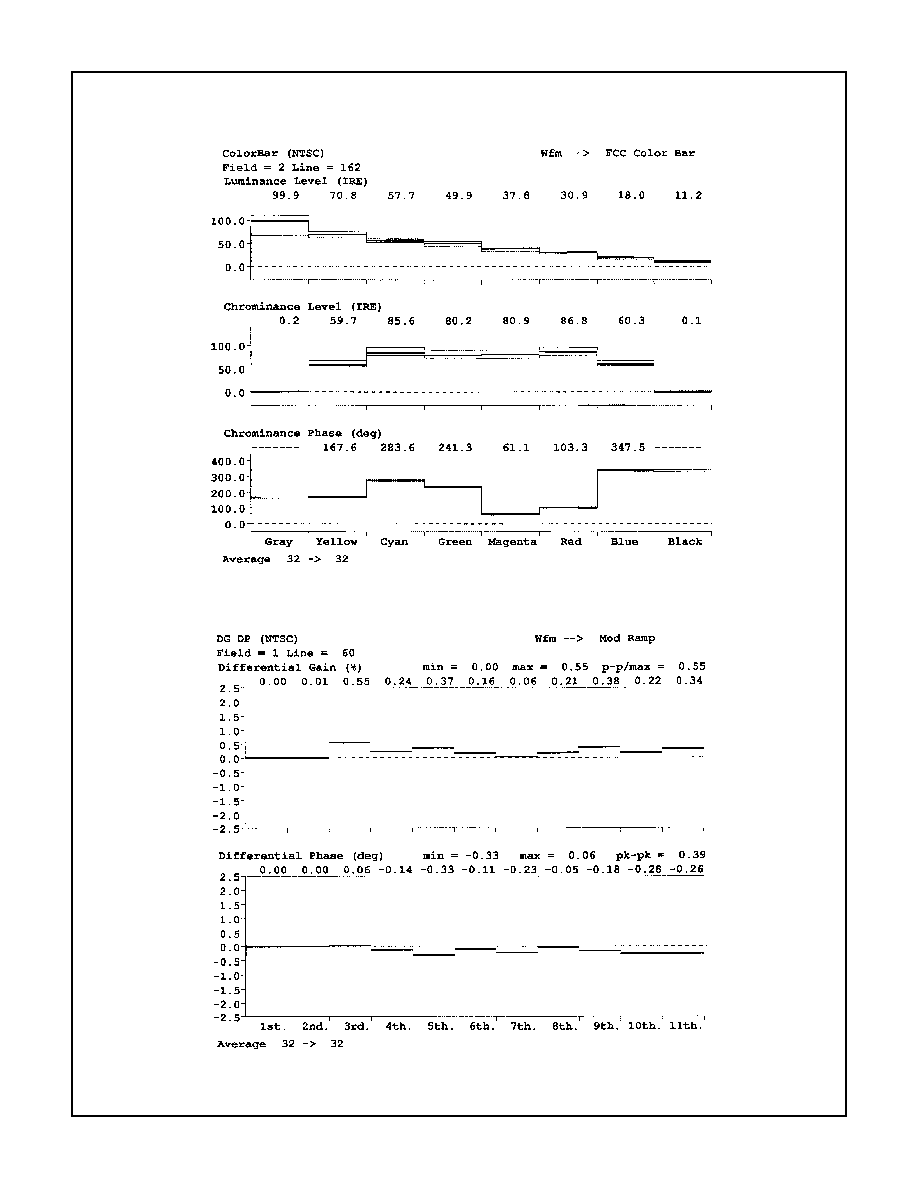
28
NTSC Composite Phase
(Continued)
FIGURE 19. COLOR BARS VM700 TEST
FIGURE 20. DIFFERENTIAL PHASE AND GAIN
Typical Performance Curves
(Continued)
HMP8112

29
NTSC Frequency Response
FIGURE 21. MULTIBURST
FIGURE 22. MULTIBURST VM700 FREQUENCY ROLL-OFF TEST
Typical Performance Curves
(Continued)
HMP8112

30
NTSC Noise Measurements
FIGURE 23. SIGNAL TO NOISE RATIO - FLAT FREQUENCY RESPONSE
FIGURE 24. SIGNAL TO NOISE RATIO - 5.0MHz LOW PASS FILTERED
Typical Performance Curves
(Continued)
HMP8112

31
NTSC Noise Measurements
(Continued)
FIGURE 25. SIGNAL TO NOISE RATIO - 4.2MHz LOW PASS FILTERED
Pixel Jitter Test
FIGURE 26. LONG TERM JITTER - 20 PULSE BAR 2T
Typical Performance Curves
(Continued)
HMP8112

32
PAL Composite Phase
FIGURE 27. COLOR BARS NTSC 100% (EIA)
FIGURE 28. COLOR BARS VECTORSCOPE
Typical Performance Curves
(Continued)
HMP8112

33
PAL Composite Phase
(Continued)
FIGURE 29. COLOR BARS VM700 TEST
FIGURE 30. DIFFERENTIAL PHASE AND GAIN
Typical Performance Curves
(Continued)
HMP8112

34
PAL Frequency Response
FIGURE 31. MULTIBURST
FIGURE 32. NTSC MULTI-TEST PATTERN
Typical Performance Curves
(Continued)
HMP8112

35
FIGURE 33. NTSC CONVERGENCE TEST PATTERN
FIGURE 34. NTSC MULTIBURST TEST PATTERN
Typical Performance Curves
(Continued)
HMP8112

36
FIGURE 35. NTSC SMPTE COLORBARS TEST PATTERN
FIGURE 36. PAL CONVERGENCE TEST PATTERN
Typical Performance Curves
(Continued)
HMP8112

37
FIGURE 37. PAL MULTIBURST TEST PATTERN
FIGURE 38. PAL SMPTE COLORBARS TEST PATTERN
Typical Performance Curves
(Continued)
HMP8112

38
FIGURE 39. CHROMINANCE AMPLIFIER GAIN vs GAIN
CONTROL VOLTAGE
FIGURE 40. LUMINANCE AMPLIFIER GAIN vs AGC CAP
VOLTAGE
Timing Waveforms
FIGURE 41. TIMING DIAGRAM
Typical Performance Curves
(Continued)
10
8
6
4
2
0
-2
-4
dB
2.6
2.8
3.0
3.2
3.4
3.6
3.8
4.0
4.2
4.4
GAIN CONTROL VOLTAGE
TEMPERATURE = 25
o
C
V
CC
= 5V
10
8
6
4
2
0
-2
-4
dB
2.6
2.8
3.0
3.2
3.4
3.6
3.8
4.0
4.2
4.4
AGC CAP VOLTAGE
TEMPERATURE = 25
o
C
V
CC
= 5V
SDA
SCL
t
BUF
t
LOW
t
HIGH
t
R
t
F
t
SU:DATA
t
HD:DATA
t
SU:STOP
HMP8112

39
PCB Layout Considerations
A PCB board with a minimum of 4 layers is recommended, with
layers 1 and 4 (top and bottom) for signals and layers 2 and 3
for power and ground. The PCB layout should implement the
lowest possible noise on the power and ground planes by pro-
viding excellent decoupling. PCB trace lengths between groups
of V
CC
and GND pins should be as short as possible.
The optimum layout places the HMP8112 as close as
possible to the power supply connector and the video output
connector.
Component Placement
External components should be positioned as close as pos-
sible to the appropriate pin, ideally such that traces can be
connected point to point. Chip capacitors are recommended
where possible, with radial lead ceramic capacitors the sec-
ond-best choice.
Power supply decoupling should be done using a 0.1
µ
F
ceramic capacitor in parallel with a 0.01
µ
F chip capacitor for
each group of V
CC
pins to ground. These capacitors should
be located as close to the V
CC
and GND pins as possible,
using short, wide traces.
Ground Plane
A common ground plane for all devices, including the
HMP8112, is recommended. All GND pins on the HMP8112
must be connected to the ground plane.
Power Planes
The HMP8112 should have its own power plane that is iso-
lated from the common power plane of the board, with a gap
between the two power planes of at least 1/8 inch. All V
CC
pins on the HMP8112 must be connected to this HMP8112
power plane. The HMP8112 power plane should be con-
nected to the board's normal V
CC
power plane at a single
point though a low-resistance ferrite bead, such as a Ferrox-
cube 5659065-3B, Fair-Rite 2743001111, or TDK BF45-
4001. The ferrite bead provides resistance to switching cur-
rents, improving the performance of HMP8112. A single
47
µ
F capacitor should also be used between the HMP8112
power plane and the ground plane to control low-frequency
power supply ripple.
If a separate linear regulator is used to provide power to the
HMP8112 power plane, the power-up sequence should be
designed to ensure latchup will not occur. A separate linear
regulator is recommended if the power supply noise on the
V
CC
pins exceeds 200mV. About 10% of the noise (that is
less than 1MHz) on the V
CC
pins will couple onto the analog
outputs.
Analog Signals
Traces containing digital signals should not be routed over,
under, or adjacent to the analog output traces to minimize
crosstalk. If this is not possible, coupling can be minimized
by routing the digital signals at a 90 degree angle to the ana-
log signals. The analog output traces should also not overlay
the HMP8112 and V
CC
power planes to maximize high-fre-
quency power supply rejection.
Evaluation Boards
The HMP8112EVAL stand-alone evaluation board allows
connecting the NTSC/PAL decoder into an IBM PC ISA slot
for evaluation. The board contains the HMP8112 NTSC/PAL
decoder, 2 Mbytes of VRAM and a encoder. The board can
accept Composite or S-Video input and display video on a
stand composite or S-Video display. The ISA bus and evalu-
ation software allows easy plug and play of the decoder for
analysis with such tools as a VM700 video test system.
HMP8112

40
HMP8112
Metric Plastic Quad Flatpack Packages (MQFP/PQFP)
D
D1
E E1
-A-
PIN 1
A2 A1
A
5
o
-16
o
5
o
-16
o
0
o
-7
o
0.40
0.016
MIN
L
0
o
MIN
PLANE
B
0.005/0.009
0.13/0.23
WITH PLATING
BASE METAL
SEATING
0.005/0.007
0.13/0.17
B1
-B-
e
0.008
0.20
A-B
S
D
S
C
M
0.10
0.004
-C-
-D-
-H-
Q80.14x20
(JEDEC MO-108CB-1 ISSUE A)
80 LEAD METRIC PLASTIC QUAD FLATPACK PACKAGE
SYM-
BOL
INCHES
MILLIMETERS
NOTES
MIN
MAX
MIN
MAX
A
-
0.134
-
3.40
-
A1
0.010
-
0.25
-
-
A2
0.100
0.120
2.55
3.05
-
B
0.012
0.018
0.30
0.45
6
B1
0.012
0.016
0.30
0.40
-
D
0.904
0.923
22.95
23.45
3
D1
0.783
0.791
19.90
20.10
4, 5
E
0.667
0.687
16.95
17.45
3
E1
0.547
0.555
13.90
14.10
4, 5
L
0.026
0.037
0.65
0.95
-
N
80
80
7
e
0.032 BSC
0.80 BSC
-
ND
24
24
-
NE
16
16
-
Rev. 0 1/94
NOTES:
1. Controlling dimension: MILLIMETER. Converted inch
dimensions are not necessarily exact.
2. All dimensions and tolerances per ANSI Y14.5M-1982.
3. Dimensions D and E to be determined at seating plane
.
4. Dimensions D1 and E1 to be determined at datum plane
.
5. Dimensions D1 and E1 do not include mold protrusion.
Allowable protrusion is 0.25mm (0.010 inch) per side.
6. Dimension B does not include dambar protrusion. Allowable
dambar protrusion shall be 0.08mm (0.003 inch) total.
7. "N" is the number of terminal positions.
-C-
-H-