
1
Semiconductor
March 1998
HMP8112A
NTSC/PAL Video Decoder
Features
∑ Supports ITU-R BT.601 (CCIR601) and Square Pixel
∑ 3 Composite Analog Inputs with Sync Tip AGC, Black
Clamping and White Peak Control
∑ Patented Decoding Scheme with Improved 2-Line
Comb Filter, Y/C Separation
∑ NTSC M and PAL (B, D, G, H, I, M, N, CN) Operation
∑ Composite or S-Video Input
∑ User-Selectable Color Trap and Low Pass Video
Filters
∑ User Selectable Hue, Saturation, Contrast, Sharpness,
and Brightness Controls
∑ User Selectable Data Transfer Output Modes
∑ 16-Bit 4:2:2 YCbCr
∑ 8-Bit 4:2:2 YCbCr
∑ User Selectable Clock Range from 20MHz - 30MHz
∑ I
2
C Interface
∑ VMI Compatible Video Data Bus
Applications
∑ Multimedia PCs
∑ Video Conferencing
∑ Video Editing
∑ Video Security Systems
∑ Digital VCRs
∑ Related Products
- NTSC/PAL Encoders: HMP8154, HMP8156A,
HMP8170/1, HMP8172/3
- NTSC/PAL Decoders: HMP8115, HMP8130/1
Description
The HMP8112A is a high quality, digital video, color decoder
with internal A/D converters. The A/D function includes a 3:1
analog input mux, Sync Tip AGC, Black clamping and two 8-
bit A/D Converters. The high quality A/D converters minimize
pixel jitter and crosstalk.
The decoder function is compatible with NTSC M, PAL B, D,
G, H, I, M, N and special combination PAL N video stan-
dards. Both composite (CVBS) and S-Video (Y/C) input for-
mats are supported. A 2-line comb filter plus a user
selectable Chrominance trap filter provide high quality Y/C
separation. Various adjustments are available to optimize the
image such as Brightness, Contrast, Saturation, Hue and
Sharpness controls. Video synchronization is achieved with
a 4xf
SC
chroma burst lock PLL for color demodulation and
line lock PLL for correct pixel alignment. A chrominance sub-
sampling 4:2:2 scheme is provided to reduce chrominance
bandwidth.
The HMP8112A is ideally suited as the analog video inter-
face to VCR's and camera's in any multimedia or video sys-
tem. The high quality Y/C separation, user flexibility and
integrated phase locked loops are ideal for use with today's
powerful compression processors. The HMP8112A operates
from a single 5V supply and is TTL/CMOS compatible.
Table of Contents
Page
Functional Block Diagrams . . . . . . . . . . . . . . . . . . . . . . . . 2
Functional Operation Introduction . . . . . . . . . . . . . . . . . . 5
Internal Register Description Tables. . . . . . . . . . . . . . . . 15
Pinout . . . . . . . . . . . . . . . . . . . . . . . . . . . . . . . . . . . . . . . 22
Pin Descriptions . . . . . . . . . . . . . . . . . . . . . . . . . . . . . . . 23
AC and DC Electrical Specifications. . . . . . . . . . . . . . . . 25
Typical Performance Curves . . . . . . . . . . . . . . . . . . . . . . 28
Applications Information . . . . . . . . . . . . . . . . . . . . . . . . . 39
Package Dimensions . . . . . . . . . . . . . . . . . . . . . . . . . . . 40
Ordering Information
PART NUMBER
TEMP.
RANGE (
o
C)
PACKAGE
PKG.NO.
HMP8112ACN
0 to 70
80 Ld PQFP
Q80.14x20
HMP8112EVAL2
PCI Reference Design (Includes Part)
HMP8156EVAL2
Frame Grabber Evaluation Board
(Includes Part)
PQFP is also known as QFP and MQFP
CAUTION: These devices are sensitive to electrostatic discharge. Users should follow proper IC Handling Procedures.
Copyright
©
Harris Corporation 1998
File Number
4407.2
NOT
RE
COM
MEN
DED
FO
R N
EW
DE
SIG
NS
See
HM
P81
15

4-2
Functional Block Diagrams
CbCr[7:0
]
Y[
7
:
0]
AC
T
I
V
E
FIELD
DV
L
D
USE
R
ADJUST
.
COL
O
R
TRAP
OUT
P
UT
SAMPLE
RA
TE
CONVE
R
TER
STD_E
R
R
LOCKED
INP
U
T
MUX
WHI
T
E PEAK LEVE
L
DIGIT
A
L COMP
AR
A
T
ORS
BLA
CK LEVEL
SY
N
C
LE
VE
L
8-
B
I
T
ADC
AG
C
CLAMP
AND
LIN0
LIN1
LI
N
2
/
Y
LC
L
A
M
P
_
C
AP
LA
GC_CAP
L_OUT
L_ADIN
+ -
CL
AMP
DIGIT
A
L C
O
MP
ARA
T
O
R
8-
B
I
T
ADC
CLAMP
CI
N
CC
LAMP_
C
A
P
GAI
N
_CT
R
L
+
-
SD
A
SC
L
RE
SET
GAIN
CONTR
O
L
LOG
I
C
AND
LI
NE
PL
L
V
SYNC
DETECT
MICR
OPR
O
CES
S
OR
INTERF
A
C
E AN
D
CONT
R
O
L
HS
YNC
VSY
NC
LO
GI
C
COLOR
DE
MODULA
T
ION
Y/
C
S
E
P
ARA
TION
INP
U
T
SA
M
P
LE
RA
TE
CONVER
TE
R
CHR
OMA
PLL
HSY
N
C
DE
T
E
CT
LOC
K
COL
O
R
ADJUST
EX
TERNAL
AN
TIALIASING
FI
L
T
ER
EX
TERNAL
A
N
TIALIASING
FI
L
T
E
R
HMP8112A

4-3
VIDEO DECODER
Functional Block Diagrams
(Continued)
Y
,
CV
BS
C
CR[7
:
0]
L[7:0
]
M U
X
IS
L
CHR
OMA
LI
NE
COMB
C,CVBS
DA
T
A
Y D
A
T
A
CHR
OMA
TRAP
ENABLE
Y D
A
T
A
CH
R
O
MA
DEMOD
U
LA
T
O
R
Y D
A
T
A
C,CV
B
S
DA
T
A
C D
A
T
A
Y D
A
T
A
UV
AG
C
U,
V
UV
SA
TURA
TION
ADJUS
T
SA
TUR
A
TI
ON
AD
J
U
S
T
SHARPNES
S
ADJUST
S
T
AND
ARD
SELE
C
T
M U
X
IS
L
HSY
N
C
DETE
C
T
CHR
OMA
PHASE
DETECT
OR
CHR
OMA
PLL NCO
4FSC
CLOCK
CLK
(20
M
H
z
- 30MHZ)
LIN
E
LOCK
ED
PLL LO
OP
FI
L
T
ER
HU
E
ADJUST
AG
C
ADJUST
V
SYNC
DETECT
INP
U
T
RA
TE
CONVE
R
TER
SAMPLE
FIL
T
ER
DELA
Y
TRAP
CbCr
DA
T
A
Y
DA
T
A
CLK T
O
4FSC RA
TIO
LO
W P
A
SS
F
I
L
T
ER ENABLE
HS
YNC
VS
YNC
ST
AN
D
ARD E
R
R
O
R
L
O
CKED
FI
ELD
SY
NC
& CONT
RAS
T
ADJUST
B
R
IGHTNES
S
,
STRI
PPE
R
,
OU
TPU
T
RA
TE
CONVE
R
TER
SA
M
P
LE
LIN
E
LOCK
ED
NCO
LP FIL
T
ER
CHR
OMA
PLL
LO
OP
FI
L
T
ER
HORIZ
O
NT
AL
AND
VE
R
T
ICAL
SHARPNES
S
ADJUST
U,
V
T
O
C
b
C
r
COLOR
CONV
ER
TER
AND COLOR
KI
LLER
SP
A
C
E
HMP8112A

4-4
Schematic
I
2
C CONTROL INTERFACE
OUTPUT INTERFACE
Functional Block Diagrams
(Continued)
SERIAL SHIFT
ADDRESS
POINTER
CONTROL
REGISTERS
....
....
....
....
A0
CONTROL
ADDRESS
POINTER
REGISTER
SDA
SCL
0x00
0x01
.
.
.
.
0x1B
DATA BUS
R
E
G
I
S
T
E
R
R
E
G
I
S
T
E
R
8
8
CbCr[7:0]
Y[7:0]
Y[7:0]
CbCr[7:0]
DVLD
OEN
M
U
X
8/16 OUTPUT
SELECT
ACTIVE
FIFO
32 X 16
DEEP
R4
75
JP1
JUMPER
V
AA
R8
50
C12
15pF
R7
10K
27MHz
64
63
60
58
57
56
55
54
Y7
Y6
Y5
Y4
Y3
Y2
Y1
Y0
Y7
Y6
Y5
Y4
Y3
Y2
Y1
Y0
65
66
67
71
70
ACTIVE
DVLD
FIELD
HSYNC
VSYNC
WPE
RESET
SDA
SCL
CLK
CLK
TEST
L_OUT
L_ADIN
LAGC_CAP
LCLAMP_CAP
CCLAMP_CAP
GAIN_CNTL
DEC_T
DEC_L
LIN0
LIN1
LIN2
CIN
U1
CbCr7
CbCr6
CbCr5
CbCr4
CbCr3
CbCr2
CbCr1
CbCr0
CB_CR7
CB_CR6
CB_CR5
CB_CR4
CB_CR3
CB_CR2
CB_CR1
CB_CR0
51
50
49
48
47
45
43
42
Y[0..7]
Y[0..7]
CB_CR[0..7]
CB_CR[0..7]
V
CC
V
CC
V
CC
V
CC
V
CC
V
CC
R9
10K
R10
10K
R11
10K
R12
10K
R13
10K
R14
4K
R15
4K
V
CC
RESET
27MHz
SCL
27
34
40
41
38
13
36
7
6
5
19
9
8
78
SDA
ACTIVE
DVLD
FIELD
VDRIVE
HDRIVE
C1
1.0
µ
F
LUMA0
CHROMA
V
AA
77
76
29
28
30
C10
0.1
µ
F
C11
0.01
µ
F
C8
0.1
µ
F
C9
0.01
µ
F
R5
1K
R6
750
C7
0.047
µ
F
C6
0.047
µ
F
C5
0.01
µ
F
R3
75
LUMA1
LUMA2/Y
R2
75
R1
75
C2
1.0
µ
F
C3
1.0
µ
F
ANTI-ALIAS
C4
1.0
µ
F
FILTER
ANTI-ALIAS
FILTER
HMP8112A
4-5
Introduction
The HMP8112A is designed to decode baseband composite
or s-video NTSC and PAL signals, and convert them to either
digital YCbCr or RGB data.
The digital PLLs are designed to synchronize to all NTSC
and PAL standards. A chroma PLL is used to maintain
chroma lock for demodulation of the color information; a line-
locked PLL is used to maintain vertical spatial alignment.
The PLLs are designed to maintain lock even in the event of
VCR headswitches.
The HMP8112A contains two 8-bit A/D converters and an
I
2
C port for programming internal registers
Analog Video Inputs
The HMP8112A supports either three composite or two
composite and one S-Video input.
Three analog video inputs (LIN0, LIN1, LIN2) are used to
select which one of three composite video sources are to be
decoded. To support S-video applications, the Y channel
drives the LIN2 analog input, and the C channel drives the
CIN analog input.
The analog inputs must be AC-coupled to the video signals,
as shown in the Applications section.
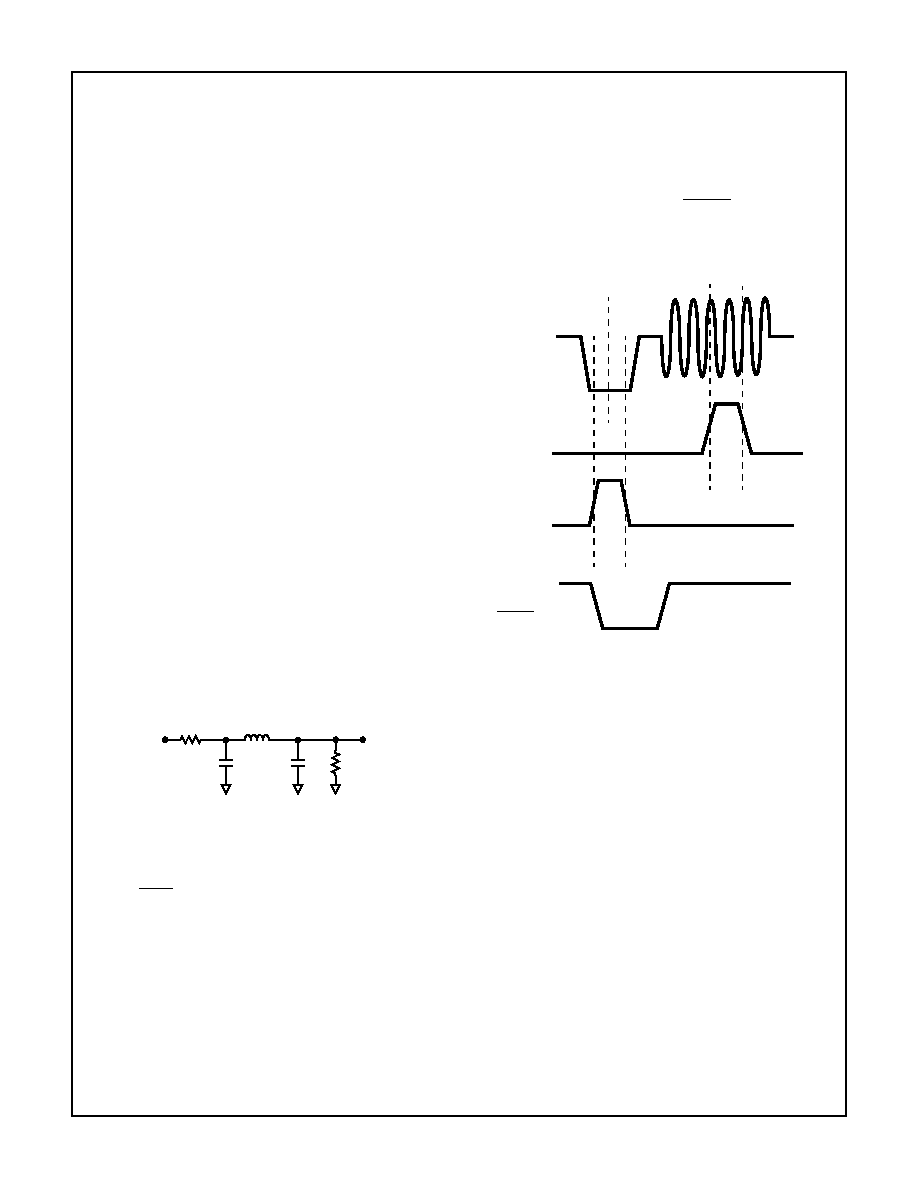
Anti-Aliasing Filter
An external anti-alias filter is required to achieve optimum
performance and prevent high frequency components from
being aliased back into the video image.
For the LIN0-2 inputs, a single filter is connected to L_OUT
and L_ADIN. For CIN the anti-aliasing filter should be con-
nected to the CIN input. A recommended filter is shown
below in Figure 1.
Luminance AGC And DC RESTORE Circuits
After a
RESET
, a change of the video standard, or a PLL
Chrominance Subcarrier Ratio Register load, the decoder
enters Acquisition Mode by attempting to lock to a new video
source. During this mode, the HAGC and DC RESTORE cir-
cuits perform continuous gain and bias adjustments until the
PLL is LOCKED onto the video signal. Once LOCKED, the
HAGC and DC RESTORE functions are performed during
programmable window periods for each horizontal video line.
The digital PLL zeroes a 10-bit pixel clock counter during
each horizontal sync tip and increments the count for each
pixel of the entire video line. The AGC amplifier attenuates or
amplifies the analog video signal during the horizontal sync
tip to maintain an average ADC code of 0. The DC
RESTORE circuit clamps the video signal during the back
porch to maintain an average ADC code of 64. Reference
Figure 2 for timing information and Table 5 for the recom-
mended register values to use for different video standards.
The START and END times of the HSYNC output are also
programmable and can be used as a reference for confirm-
ing proper HAGC and DC RESTORE timing.
White Peak Enable
The white peak enable input, (WPE) enables or disables the
white peak control of the luminance input. If enabled, the
AGC will reduce the gain of the video amplifier when the dig-
ital outputs exceed code 248 to prevent over-ranging the
A/D. If disabled, the AGC operates normally, keeping the hor-
izontal sync tip at code 0 and allowing the A/D's range to go
to 255 at the maximum peak input.
Chrominance Input
The chrominance amplifier gain control is manually set by a
voltage applied to the GAIN_CNTL pin. Refer to Figure 3
below for gain characteristics. The chrominance channel
also has a digital AGC which can drive the color reference
burst to a nominal +-20 IRE. This function is enabled by
default on reset, but can be disabled using the Video Input
Control register. The chrominance input is clamped during
the DC RESTORE window to maintain an average ADC
code of 128.
FIGURE 1. RECOMMENDED ANTI-ALIASING FILTER
R1
332
R2
4.02K
C2
82pF
L1
8.2
µ
H
C1
33pF
FIGURE 2. DC RESTORE AND HAGC TIMING
VIDEO INPUT
HAGC
DC RESTORE
START
TIME
END
TIME
START
TIME
END
TIME
0
HSYNC
HSYNC
START
TIME
END
TIME
HMP8112A

4-6
Reset
The RESET pin is used to return the decoder to an
initialization state. This pin should be used after a power-up
to set the part into a known state. The internal registers are
returned to their RESET state and the Serial I
2
C port is
returned to inactive state. The RESET pin is an active low
signal and should be asserted for minimum of 1 CLK cycle.
After a RESET or a software reset has occurred all output
pins are three-stated. The VSYNC, HSYNC, DVLD, ACTIVE
and FIELD output pins must be pulled high to ensure proper
operation. A 10K or smaller pullup resistor to V
CC
is
recommended.
NTSC/PAL Decoder
The NTSC/PAL decoder is designed to convert incoming
Composite or Separated (SVHS, Y/C) video into it's YCbCr
component parts. The digital phase locked loops are
designed to synchronize to the various NTSC/PAL stan-
dards. They provide a stable internal 4xf
SC
(Frequency of
the Color Sub-Carrier) video clock for color demodulation,
and a line locked clock for vertical spatial pixel alignment.
The decoder uses the CLK to run the A/D converters and the
phase locked loops. This asynchronous master clock for the
decoder eliminates the need for a unique clock source in a
Multimedia application. CLK can run from 20MHz to 30MHz
when using the 16-bit Synchronous Data output Mode. The
user must program the CLK to Color Sub-Carrier Ratio to
match the CLK frequency used (see Internal Phase Locked
Loops discussion). When using the 8-bit Burst Data Output
Mode the CLK should be a 24.54MHz, 27MHz or 29.5MHz
depending on the output video standard chosen. The crystal
oscillator must have a ±50ppm accuracy and a 60/40% duty
cycle symmetry to ensure proper operation. Since the video
data from the external A/D's are sampled at the CLK fre-
quency a sample rate converter is employed to convert the
data from the CLK rate to the internal decoding frequency of
4xfSC.
The input sample rate converter will interpolate between
existing CLK samples to create the chroma locked (4xf
SC
)
samples needed for the color decoder. An interpolation is
done to create the 4xf
SC
pixel and a correction factor is then
applied.
The decoder can be used with the following video sources:
Analog Composite - NTSC M, - PAL B, D, G, H, I, N
And Special Combination PAL N
Analog S - VHS (Y/C) - NTSC M, PAL B, D, G, H, I, N
And Special Combination PAL N
Color Separation, and Demodulation
To separate the chrominance modulated color information
from the baseband luminance signal, a 2-Line comb filter is
employed. In NTSC signals the color information changes
phase 180
o
from one line to the next. This interleaves the
chrominance information at half line intervals throughout the
NTSC video spectrum. Therefore, NTSC has 227.5 cycles of
chrominance per NTSC line. The half of a cycle causes the
next reference burst to be 180
o
out of phase with the previ-
ous line's burst. The 2-Line comb efficiently removes the
chrominance information from the baseband luminance sig-
nal. When decoding NTSC, the decoder maintains full lumi-
nance bandwidth horizontally throughout the chrominance
carrier frequency range. Unlike most 2 line comb filter sepa-
ration techniques, vertical bandwidth is maintained by
means of a proprietary transform technique.
Reset
The RESET pin is used to return the decoder to an initializa-
tion state. This pin should be used after a power-up to set the
part into a known state. The internal registers are returned to
their RESET state and the Serial I
2
C port is returned to inac-
tive state. The RESET pin is an active low signal and should
be asserted for minimum of 1 CLK cycle. After a RESET or a
software reset has occurred all output pins are three-stated.
The VSYNC, HSYNC, DVLD, ACTIVE and FIELD output pins
must be pulled high to ensure proper operation. A 10K or
smaller pullup resistor to V
CC
is recommended.
7
6
5
4
3
2
1
0
LI
NEA
R
G
A
IN
1.6
1.8
2.0
2.2
2.4
2.6
2.8
3.0
3.2
3.4
GAIN CONTROL VOLTAGE
TEMPERATURE = 25
o
C
V
CC
= 5V
FIGURE 3. CHROMINANCE AMPLIFIER GAIN
TIME
INCOMING VIDEO SAMPLES
TIME
RESAMPLED VIDEO
4xf
SC
FIGURE 4. SAMPLE RATE CONVERSION
HMP8112A

4-7
For PAL systems there are 283.75 cycles of chrominance
per line. Chrominance information is spaced at quarter line
intervals with a reference phase of 135
o
. The reference
phase alternates from line to line by 90
o
. To fully separate
the PAL chrominance and luminance signals the user select-
able filters should be enabled. The chroma notch filter built
into the luminance channel should be enabled for PAL sys-
tems to reduce cross luminance effects. The low pass filter in
the chrominance processing chain helps to reduce cross
color products.
The demodulator in the decoder decodes the color compo-
nents into U and V. The U and V components are converted
to Cb
and Cr components after the decoding process.
YCbCr has a usable data range as shown in Figure 7. The
data range for Y is limited to a minimum of 16.
The decoder is compatible with all NTSC and PAL video for-
mats available throughout the world. Table 2 shows the com-
patible video standards.
Horizontal Sync Detection
Horizontal sync is detected in the Output Sample Rate con-
verter (OSR). The OSR spatially aligns the pixels in the verti-
cal direction by using the horizontal sync information
embedded in the digital video data stream. The HSYNC
sync pulse out of the decoder is a video synchronous output
pin. This signal follows the horizontal sync of an input video
source. If there is no source the HSYNC pin will continue to
run at video rates due to the Line Locked PLL free-running.
HSYNC can be moved throughout the video line using the
HSYNC Start and End time registers. This 10-bit register
allows the HSYNC to be moved in OSR clock increments
(12.27MHZ, 13.5MHz or 14.75MHz).
Vertical Sync and Field Detection
The vertical sync and field detect circuit of the decoder uses
a low time counter to detect the vertical sync sequence in
the video data stream. The low time counter accumulates
the low time encounted after the horizontal sync edge or at
the start of each line. When the low time count exceeds the
vertical sync detect threshold, VSYNC is asserted immedi-
ately. VSYNC will remain asserted for a minimum of 1 line.
The FIELD flag is updated at the same time as the VSYNC
line. The FIELD pin is a `0' for ODD fields and a `1' for even
fields.
In the case of lost vertical sync or excessive noise that would
prevent the detection of vertical sync, the FIELD flag will
continue to toggle. Lost vertical sync is declared if after 337
lines a vertical sync period was not detected for 3 successive
lines. When this occurs the phase locked loops are initialized
to the acquisition state.
The VSYNC pulse out of the decoder follows the vertical
sync detection and is typically 6.5 lines long. The VSYNC
will run at the field rate of the selected video standard
selected. For NTSC the field rate is 60Hz and for PAL the
field rate is 50Hz. This signal will continue to run even in the
event of no incoming video signal.
FREQUENCY
AMPLITUDE
f
H
/2
f
H
/2
f
H
Y
I, Q
Y
FREQUENCY
AMPLITUDE
Y
Y
I, Q
FIGURE 5. COMPOSITE NTSC INTERLEAVE SCHEME
FREQUENCY
AMPLITUDE
f
H
/4
f
H
Y
I, Q
Y
FREQUENCY
AMPLITUDE
Y
Y
f
H
/4
I, Q
I, Q
I, Q
FIGURE 6. COMPOSITE PAL INTERLEAVE SCHEME
Y DATA
RANGE
Cb DATA
RANGE
Cr DATA
RANGE
16
128
248
255
0
16
128
240
255
0
16
128
240
255
212
44
212
44
BLACK
WHITE
100%
BLUE
100%
BLUE
75%
YELLOW
100%
YELLOW
75%
RED
100%
RED
75%
CYAN
100%
CYAN
75%
FIGURE 7. YCbCr DATA RANGES
HMP8112A

4-8
Internal Phase Locked Loops
The HMP8112A has two independent digital phase locked
loops on chip. A chroma phase-locked loop is implemented
to maintain chroma lock for demodulation of the color chan-
nel, and a line locked phase lock loop is implemented to
maintain vertical spatial alignment. The phase locked loops
are designed to maintain lock even in the event of VCR
headswitches.
The HMP8112A can use a main crystal (CLK) of 20MHz to
30MHz. The crystal is used as a reference frequency for the
internal phase locked loops. The ratio of the crystal fre-
quency to the video standard is programmed into an internal
register for the PLLs to correctly decode video.
The HMP8112A decoder contains 2 sample rate converters
and 2 phase locked loops that lock to the incoming video.
The input sample rate converter synchronizes the digitized
video from the CLK rate to a 4xfSC rate. The chrominance is
separated from the luminance and then demodulated.
The Chroma PLL uses the CLK source as a reference fre-
quency. To initialize the Chroma PLL, the CLK to 4xfSC ratio
value must be loaded into the Chroma PLL Ratio Register
pair. A default 16-Bit Fractional Chroma PLL Ratio Value of
0x87C1 is used after a system RESET is applied. Refer to
Table 1 for example PLL Ratio values to use with the sup-
ported video standards 27MHz or 24.54MHz clocks. Using a
different CLK will require different values to be calculated per
the method shown below. The default assumes a CLK of
27MHz and NTSC as the video standard, and is calculated
as follows:
Ratio =
(4 x fSC) / CLK
=
(4 x 3.579545MHz) / 27MHz
=
0.530303
Register Data: Ratio * 65536
0.530303 * 65536 = 34753.94
Hex Conversion:
0x87C1
The Output Sample Rate converter is locked to the horizon-
tal line frequency and is used to spatially align pixels in a
field. The LOCKED flag signals when the phase locked loop
is within a
±
4 pixel range of the horizontal sync edge. When
line errors exceed that range the LOCKED flag is cleared.
In cases where VCRs are used in Pause, Fast Forward or
Fast Reverse, lines are typically dropped or added by the
VCR. In a worst case scenario a VCR line tolerance will vary
by
±
8%. The standard detect logic checks the line count
against the given standard to determine an error. VCRs in
trick mode cannot cause a standard error. With an NTSC
standard VCR the number of lines in a field should not
O
V
VIDEO
LOW TIME
VSYNC
FIELD
VSYNC DETECT THRESHOLD
`EVEN' FIELD
COUNTER
APPROX. 5.75 LINES
FIGURE 8. VSYNC TIMING AND THE EVEN TO ODD FIELD TRANSITION
`ODD' FIELD
HSYNC
INPUT
1
LINE #
2
3
4
5
6
7
8
9
10
525
524
1
2
3
4
5
FIGURE 9. VSYNC TIMING AND THE ODD TO EVEN FIELD TRANSITION
O
V
VIDEO
LOW TIME
VSYNC
FIELD
VSYNC DETECT THRESHOLD
`ODD' FIELD
COUNTER
APPROX. 6.25 LINES
`EVEN' FIELD
HSYNC
INPUT
264
LINE #
265
266
267
268
269
270
271
272
273
263
262
1
2
3
4
5
6
HMP8112A

4-9
exceed 285. Greater than 285 lines in a field is interpreted
as a PAL video source. An ideal NTSC source should have
262.5 lines per field and a PAL source should have 312.5
lines per field.
The HMP8112A can detect a STANDARD ERROR that sig-
nals when the video received does not match the standard
that was programmed into the Video Input Control Register.
This flag, when asserted, tells the user that the video stan-
dard that was expected was not found and a different stan-
dard should be selected in the Video Input Control register.
The error flag is cleared after a RESET or after the Chroma
PLL Clock Ratio register has been loaded via the I
2
C bus.
After the flag is cleared the standard error logic verifies the
video standard. The error flag is set after 2 vertical sync peri-
ods have passed and the line count did not match the
expected line count.
Video Adjustments
The HMP8112A allows the user to vary such video parame-
ters as Contrast, Brightness, Sharpness, Hue and Color Sat-
uration. These adjustments can be made via the I
2
C
interface. Contrast, brightness and sharpness are luminance
controls. The full dynamic range of the luminance channel
can be used by selecting the IRE setup cancellation mode.
This mode will remove the IRE setup and blanking level off-
set to take advantage of the full dynamic range of the lumi-
nance processing path. The sharpening filters allow the
enhancement of low, mid and high frequency components of
the luminance signal to compensate for low amplitude video.
Vertical sharpness is also controlled via the I
2
C interface.
Hue and Color saturation controls enhance the CbCr compo-
nents of the incoming video, all under user control.
Luminance Adjustments
The Luminance data can be adjusted in the HMP8112A. The
user can adjust brightness and contrast of the Y or lumi-
nance data. The user can also set the IRE or setup subtrac-
tion value to eliminate the black pedestal offset from NTSC
signals. The Contrast adjustment range can exceed a value
of one so as to take full advantage of the 8-bit dynamic range
for Y. The user control settings executes the equation
Y
OUT
= (Y - IRE Setup + BRIGHTNESS) x CONTRAST
Brightness
The user can control the brightness of the incoming video by
programming the Brightness register. The brightness adjust-
ment will offset the Y component. The brightness register is
an 8-bit register where the bottom 7 bits are brightness con-
trol and the top bit enables NTSC 7.5 IRE black setup can-
cellation.
When the IRE bit is set (1) for NTSC, then 73 is subtracted
from the Y data. If the IRE bit is cleared (0) for PAL, then 64
is subtracted. The brightness control bits BR[6-0] will
brighten the picture as the value is increased. BR = -64 is the
darkest and BR = +63 is the brightest. The default value of
the register after a RESET is 0 (80
H
).
Contrast
The contrast adjustment will allow the user to increase and
decrease the gain of the Y data. The contrast factor is an 8-
bit number (as shown below) that ranges from 0 to 1.992.
X.XXXXXXX
The default register value of 1.4766 (0xBD) is calculated as
follows:
Register = Factor * 128 = 1.4766 * 128 = 189 = 0xBD
TABLE 1. COMPATIBLE VIDEO INPUT STANDARDS
STANDARD
COLOR
SUBCARRIER
f
SC
27MHz
PLL
Ratio
24.54MHz
PLL
Ratio
FIELDS/
SECOND
VERTICAL
LINES
LINE
FREQUENCY
NOMINAL
BANDWIDTH
BLACK
SETUP TO
BLANK
NTSC
(M)
3.579545MHz
0x87C1
0x955D
60Hz
525
15,734
(
±
0.0003%)
4.2MHz
7.5 IRE
PAL
(B, D, G, H, I)
4.43361875MHz
0xA826
0xB901
50Hz
625
15,625
(
±
0.02%)
5.0MHz
0 IRE
PAL
(M)
3.57561149MHz
0x879B
0x9533
60Hz
525
15,750
(
±
0.0003%)
4.2MHz
7.5 IRE
PAL
(N)
4.43361875MHz
0xA826
0xB901
50Hz
625
15,625
(
±
0.15%)
4.2MHz
7.5 IRE
PAL Special
Combination N
3.58205625MHz
0x97DA
0x9578
50Hz
625
15,750
(
±
0.15%)
4.2MHz
7.5 IRE
IRE BLACK SETUP
+
+
-
X
BRIGHTNESS
CONTRAST
Y DATA
FROM
DECODER
Y'
8
FIGURE 10. LUMINANCE CONTROL SETTINGS PATH
(0 TO 1.999)
(NTSC = 73, PAL = 64)
(-64 TO +63)
HMP8112A

4-10
Hue or Tint Adjust
The Hue adjustment is applied to the U and the V color dif-
ference signal. The Hue adjusts the phase of the given UV
data. The Hue can be adjusted by ±30 degrees in 1/4 degree
increments. This is achieved by changing the Burst Phase
Locked reference point. Figure 11 shows the block diagram
for the color adjustment section. This default value for this
register is 0.
Horizontal/Vertical Sharpness
The frequency characteristics of the video waveform can be
altered to enhance the sharpness of the picture. The Hori-
zontal Sharpness register acts as a 4 band equalizer where
the amplitude of specific frequency ranges can be
enhanced or diminished. The Sharpness Control Register
allows the Low (LF), Mid (MF) and High Frequency (HF)
bands of the luminance signal to be enhanced. Vertical
Sharpness can be adjusted to 1 or a factor of 0. The
RESET default is a factor of 1.0
The 2-bit values allow 4 choices of scaling factors. The
sharpness control helps to compensate for losses in the
scaling interpolators that can reduce the amplitude of high
frequency components.
The Color Killer
(AGC Hysteresis and Loop Limits)
The color killer will disable the color difference path and set
the U and V components to zero. The automatic color killer
circuitry uses the AGC threshold to determine the maximum
and minimum gain factor limits. The loop filter determines
how much the AGC gain factor can be changed within one
line. The maximum gain factor (Max = 8) and the minimum
gain factor (Min = 0.5) will limit the range of the AGC. When
the gain factor exceeds the maximum gain factor of 8, the
gain factor is limited to 8. Once the signal has an amplitude
of 1/16th, the nominal video the color killer is enabled and
the chroma phase locked loop holds it's last phase refer-
ence. While the color killer is enabled, the U and V compo-
nents are forced to zero. Once the input video signal reaches
1/7th the optimum amplitude the color killer is disabled and
the color is returned.
The dynamic range of the AGC allows it to compensate for
video that is 1/8 to 2 times the specified nominal of 1V
P-P
.
Saturation
The color saturation component is controlled via the Color
Saturation Registers. The color saturation is applied to the
UV components after the AGC function. The saturation value
is multiplied by the UV data to increase the color intensity.
This is an 8-bit number (as shown below) that ranges from 0
to 1.992.
X.XXXXXXX
The default register value of 1.2266 (0x9D) is calculated as
follows:
Register = Factor * 128 = 1.2266 * 128 = 157 = 0x9D
TABLE 2. SHARPNESS GAIN FACTOR SELECTS
XF1
XF0
GAIN FACTOR
0
0
Scaled By 1.0
0
1
Scaled By 2.0
1
0
Scaled By 4.0
1
1
Scaled By 0
DEMODULATED
UV DATA
UV DATA
VIDEO
DATA
HUE OFFSET
HUE
ADJUST
+
TO INPUT SAMPLE
RATE
CONVERTER
LOOP
CHROMA
PHASE LOCKED
COLOR
DECODER
CHROMA
AGC AND
USER
SETTINGS
FIGURE 11. HUE ADJUST BLOCK DIAGRAM
˜
4096
FACTOR
GAIN
MIN
I
2
C
COLOR
KILLER
LINE
COUNT
UV
DATA
AGC
ENABLE
FIGURE 12. LOOP FILTER BLOCK DIAGRAM (HYSTERESIS)
FACTOR
GAIN
MAX
AGC
GAIN
FACTOR
HMP8112A
4-11
Output Data Port Modes
The HMP8112A can output data in 2 formats, an 8-bit Pixel
Transfer Mode and a 16-bit Pixel Transfer mode.
16-Bit Pixel Transfer Mode
In 16-bit Pixel Transfer Mode pixel data is output at the CLK
frequency and Table 3 shows the number of data points per
video line to expect for a given standard. Data is output as
4:2:2 subsampled data in a Y-Cb/Y-Cr 16-bit sequence. The
Data Valid (DVLD) flag is asserted when video data is
present on the 16-bit output port (Y[7:0], CbCr[7:0]). The
luminance data is output on Y[7:0] bus. Chrominance data is
sequenced on the CbCr[7:0] bus, starting with Cb and then
Cr. Per Figure 13, the ACTIVE flag is asserted when the
active video portion of the horizontal scan line is present on
the data output port. See Figure 14 for 16-Bit Pixel Transfer
Mode timing. DVLD is asserted every time the output sample
rate converter has a valid output. When DVLD and ACTIVE
are used together the visual portion of the image can be
captured. When DVLD is used alone all valid data during the
Horizontal, Vertical and Reference Burst Timing are
available.
The CLK can be run on a 20MHz - 30MHz clock source.
Data will be output (on average) at the Output Data Rate
shown in Table 3 for a given standard. Data is clocked out
synchronous to CLK and will come in bursts. To smooth out
the data output to a regular rate, a CLK of 2X the average
output data rate can be used.
8-Bit Pixel Transfer Mode
For 8-Bit Pixel Transfer Mode the Y[7:0] output bus is used to
transfer all YCbCr data. The data is 4:2:2 subsampled but
will only contain the active video portion of the line. See Fig-
ure 15 for 8-Bit Pixel Transfer Mode timing. In this mode, the
data is clocked out at the CLK rate and only clock frequen-
cies of 24.54MHz, 27MHz and 29.5MHz can be used. In 8-
bit Mode, the data is sequenced on the Y[7:0] bus in Cb, Y,
Cr, Y format. ACTIVE is asserted as soon as the mode is
selected. DVLD when asserted, indicates a valid active pixel
is available. Pixels during the horizontal and vertical blanking
are not available. Only the active portions of the video line
are output.
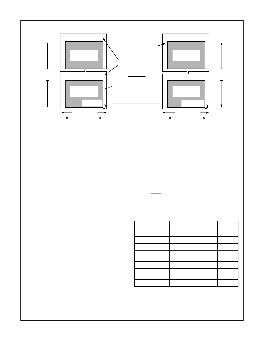
FIGURE 13. ACTIVE VIDEO REGIONS
LINES 1 - 22 NOT ACTIVE
NTSC M, PAL M
PAL B, D, G, H, I, N, COMB N
ODD FIELD
LINES 263 - 284 NOT ACTIVE
EVEN FIELD
LINES 1 - 22 NOT ACTIVE
LINES 311 - 335 NOT ACTIVE
858
NUMBER OF PIXELS
TOTAL PIXELS
ACTIVE PIXELS
720
(780)
(640)
864
TOTAL PIXELS
ACTIVE PIXELS
720
(944)
(768)
RECTANGULAR (SQUARE)
SYNC AND
BACK
PORCH
FRONT
PORCH
VERTICAL
BLANKING
NTSC
PAL
480 ACTIVE
LINES/FRAME
(NTSC, PAL M)
576 ACTIVE
LINES/FRAME
(PAL)
(LINES 23-262)
240 ACTIVE LINES
PER FIELD
(LINES 285 - 524)
240 ACTIVE LINES
PER FIELD
LINE 525
NOT ACTIVE
(LINES 23 - 310)
288 ACTIVE LINES
PER FIELD
LINES 624-625
NOT ACTIVE
(LINES 336 - 623)
288 ACTIVE LINES
PER FIELD
TABLE 3. OUTPUT MODE STANDARDS
STANDARD
OUTPUT
DATA
RATE
TOTAL
PIXELS
(WITH SYNCS)
ACTIVE
PIXELS
NTSC Square Pixel
12.27MHz
780 x 525
640 x 480
NTSC CCIR 601
13.5MHz
858 x 525
720 x 480
PAL B, D, G, H, I, N,
COMB N, CCIR601
13.5MHz
864 x 625
720 x 576
PAL M CCIR 601
13.5MHz
858 x 525
720 x 480
PAL B, D, G, H, I, N
Square Pixel
14.74MHz
944 x 625
768 x 576
PAL M Square Pixel
14.74MHz
780 x 525
640 x 480
HMP8112A

4-12
NOTES:
1. Y
0
is the first active luminance pixel of a line. Cb
0
and Cr
0
are first active chrominance pixels in a line. Cb and Cr will alternate every cycle
due to the 4:2:2 subsampling. Y
N
the last valid pixel in the blanking period.
2. ACTIVE is asserted per Figure 13.
3. DVLD is asserted for every valid pixel during both active and blanking regions. DVLD is not a 50% duty cycle synchronous output and will
appear to jitter as the Output Sample Rate converter adjusts the output timing for various data rates and clock frequency inputs.
FIGURE 14. OUTPUT TIMING 16-BIT MODE
Y
0
Y
N
Cb
0
Cr
N
Y
1
Cr
0
Y
2
Cb
2
Y
3
Cr
2
Y
4
Cb
4
CLK
DVLD
ACTIVE
Y[7-0]
CbCr[7-0]
t
DVLD
NOTE 1
NOTE 2
NOTE 3
CLK
DVLD
ACTIVE
Y[7-0]
t
DVLD
Cb
0
Y
0
Cr
0
Cb
2
Y
2
Cr
2
Y
1
Y
3
Cb
4
NOTES:
4. Y
0
is the first active luminance pixel of a line. Cb
0
and Cr
0
are first active chrominance pixels in a line. Cb and Cr will alternate every cycle
due to the 4:2:2 subsampling. Pixel data is not output during the blanking period.
5. ACTIVE stays asserted as soon as 8-Bit mode is selected.
6. DVLD is asserted for every valid pixel during the active region only per Figure 13. DVLD may deassert briefly during the active video region
as the Output Sample Rate converter adjusts the output timing for various data rates and clock frequency inputs.
FIGURE 15. OUTPUT TIMING 8-BIT MODE
NOTE 6
NOTE 4
NOTE 5
HMP8112A

4-13
I
2
C Control Interface
The HMP8112A utilizes an I
2
C control bus interface to pro-
gram the internal configuration registers. This standard
mode (up to 100 KBPS) interface consists of the bidirectional
Serial Data Line (SDA) and the Serial Clock Line (SCL). The
implementation on the HMP8112A is a simple slave interface
that will not respond to general calls and cannot initiate a
transfer. The SDA and SCL control pins should be pulled
high through external 4k
pullup resistors to
V
CC
.
The I
2
C clock/data timing is shown below in Figure 16. The
HMP8112A always uses chip address 0x88. There are 28
internal registers used to program and configure the
decoder. The I
2
C control port contains a pointer register that
auto-increments through the entire register space and can
be written. The autoincrement pointer will wrap after the last
register has been accessed (Product ID Register) and
should be set to the desired starting address each time an
access is started. For a write transfer, the I
2
C device base
address is the first part of a serial transfer. Then the internal
register pointer is loaded and a series of registers can be
written. If multiple registers are written, the pointer register
will autoincrement up through the register address space. A
stop cycle is used to end the transfer after the desired num-
ber of registers are programmed.
For a read transfer, the I
2
C device address is the first part of
the serial transfer. Then the internal register pointer is
loaded. At this point another start cycle is initiated to access
the individual registers. Figure 18 shows the programming
flow for read transfer of the internal registers. Multiple regis-
ters can be read and the pointer register will autoincrement
up through the pointer register address space. On the last
data read, an acknowledge should not be issued. A stop
cycle is used to end the transfer after the desired number of
registers are read.
The HMP8112A contains a product ID register that can be
used to identify the presence of a board during a Plug 'n Play
detection software algorithm. The Product ID Code register is
at sub address 0x1B and always returns a data value of 0x12.
FIGURE 16. I
2
C TIMING DIAGRAM
SDA
SCL
t
BUF
t
LOW
t
HIGH
t
R
t
F
t
SU:DATA
t
HD:DATA
t
SU:STOP
SDA
SCL
START
CONDITION
S
1-7
ADDRESS
8
R/W
9
ACK
1-7
DATA
8
9
ACK
STOP
CONDITION
P
FIGURE 17. I
2
C SERIAL DATA FLOW
S = START CYCLE
P = STOP CYCLE
A = ACKNOWLEDGE
FROM MASTER
FROM HMP8112A
0x88
DATA WRITE
DATA
DATA
0x88
DATA READ
NA = NO ACKNOWLEDGE
0x89
1000 1000 (R/W)
1000 1000
FIGURE 18. REGISTER WRITE/READ FLOW
S
CHIP ADDR
A
SUB ADDR
DATA
DATA
P
NA
CHIP ADDR
S
SUB ADDR
CHIP ADDR
S
P
A
A
A
A
A
A
REGISTER
POINTED
TO BY
SUB ADDR
OPTIONAL FRAME
MAY BE REPEATED
n TIMES
A
REGISTER
POINTED
TO BY
SUB ADDR
OPTIONAL FRAME
MAY BE REPEATED
n TIMES
HMP8112A

4-14
/
TABLE 4. DEFAULT REGISTER VALUES
SUB
ADDR
(HEX)
REGISTER NAME
DEFAULT
VALUE
(HEX)
USE
VALUE
(HEX)
Comments
0x00
0x01
0x02
0x03
0x04
0x05
0x06
0x07
0x08
0x09
0x0A
0x0B
0x0C
0x0D
0x0E
0x0F
0x10
0x11
0x12
0x13
0x14
0x15
0x16
0x17
0x18
0x19
0x1A
0x1B
Video Input Control
Luminance Brightness Control
Luminance Contrast Adjust
Hue Adjust
Luminance Sharpness Control
Color Saturation Adjust
PLL Clock Frequency Ratio (LSB)
PLL Clock Frequency Ratio (MSB)
HAGC Start Time (LSB)
HAGC Start Time (MSB)
HAGC End Time (LSB)
HAGC End Time (MSB)
HSYNC Start Time (LSB)
HSYNC Start Time (MSB)
HSYNC End Time (LSB)
HSYNC End Time (MSB)
PLL Adjust
PLL Sync Detect Window
DC RESTORE Start Time (LSB)
DC RESTORE Start Time (MSB)
DC RESTORE End Time (LSB)
DC RESTORE End Time (MSB)
Output Format Control
Software Reset and Video Status
Reserved
Reserved
Reserved
Product ID
0xF8
0x80
0xBD
0x00
0x00
0x9D
0xC1
0x87
0x3F
0x03
0x00
0x00
0x3B
0x03
0x20
0x00
0x00
0xDD
0x37
0x00
0x52
0x00
0x00
0x00
0x00
0x00
0x00
0x12
Table 1
Table 1
Table 5
Table 5
Table 5
Table 5
Table 5
Table 5
Table 5
Table 5
0x20
0x20
Table 5
Table 5
Table 5
Table 5
Defaults to NTSC and Mux = LIN0
Defaults to NTSC with 27MHz Clock Ratio
Recommend PLL Adjust = 0x20
Recommend PLL Sync Detect Window = 0x20
Bits 6-2 define Output Mode.
Set Bit 7 to Reset.
TABLE 5. RECOMMENDED TIMING REGISTER CONFIGURATION
VIDEO
STANDARD
(ACTIVE PIXELS)
TOTAL
PIXELS
PER
LINE
LAST
PIXEL
COUNT
(HEX)
HAGC WINDOW
(SYNC TIP)
DC RESTORE WINDOW
(BACK PORCH)
HSYNC WINDOW
(BLANKING INTERVAL)
START
END
START
END
START
END
REGISTERS
MSB/LSB
0x09/0x08
REGISTERS
MSB/LSB
0x0B/0x0A
REGISTERS
MSB/LSB
0x13/0x12
REGISTERS
MSB/LSB
0x15/0x14
REGISTERS
MSB/LSB
0x0D/0x0C
REGISTERS
MSB/LSB
0x0F/0x0E
NTSC, CCIR601
Rectangular Pixel
(720 x 480)
858
0x0359
0x033B
0x001B
0x002D
0x0048
0x033B
0x0060
NTSC
Square Pixel
(640 x 480)
780
0x030B
0x02F0
0x0014
0x0028
0x0040
0x02F0
0x0050
PAL-B, CCIR601
Rectangular Pixel
(720 x 576)
864
0x035F
0x0345
0x001A
0x0032
0x0050
0x0345
0x0070
PAL-B
Square Pixel
(768 x 576)
944
0x03AF
0x0392
0x001C
0x0044
0x0056
0x0392
0x0070
HMP8112A

4-15
TABLE 6. VIDEO INPUT CONTROL
SUB ADDRESS = 0x00
BIT
NUMBER
FUNCTION
DESCRIPTION
RESET
STATE
7 - 6
Video Input
Standard
These bits select the video input standard.
00 = PAL B, G, H, I, N; 4.43MHz subcarrier; 50fps; 625 lines/frame;
01 = PAL M; 3.58MHz subcarrier; 60fps; 525 lines/frame;
10 = Special PAL N; 3.58MHz subcarrier; 50fps; 625 lines/frame;
11 = NTSC M; 3.58MHz subcarrier; 60fps; 525 lines/frame (default);
11
B
5
Color Trap Filter
Disable
This bit enables the color subcarrier trap filter. The filter removes the color subcarrier infor-
mation from the luminance channel. The filter should be enabled for PAL Standard systems.
0 = Enabled
1 = Disabled (default)
1
B
4
Chrominance Low
Pass Filter Disable
This bit enables the chrominance low pass filter. This filter band limits the chrominance
channel to remove luminance artifacts. This filter should be enabled for PAL Standard
systems.
0 = Enabled
1 = Disabled (default)
1
B
3
Automatic Color
Gain Control
This bit enables the color AGC function. When this bit is set the color AGC will automati-
cally adjust the chrominance channel gain, to drive the color reference burst to a nominal
±
20 IRE's. When this bit is cleared the color AGC gain factor is set to 1.0 and the color
saturation must be adjusted to obtain nominal CrCb values.
0 = Disabled
1 = Enabled (default)
1
B
2 - 1
A/D Converter
Multiplexer Selects
These bits control the A/D input select multiplexers and whether S-Video is being input as
follows:
0, 0 = Select Composite Video Input = LIN0 (Pin 7), set decoder for Composite
1, 0 = Select Composite Video Input = LIN1 (Pin 6), set decoder for Composite
0, 1 = Select Composite Video Input = LIN2 (Pin 5), set decoder for Composite
1, 1 = Select S-Video Y Input = LIN2 (Pin 5) and C Input = CIN (Pin 19)
00
B
0
Not Used
Write Ignored, Read 0's
0
B
TABLE 7. LUMINANCE BRIGHTNESS CONTROL
SUB ADDRESS = 0x01
BIT
NUMBER
FUNCTION
DESCRIPTION
RESET
STATE
7
IRE Setup
Cancellation Control
This bit enables the black setup cancellation circuit for NTSC sources. When this bit is set
a value of 73 is used to strip the sync information from the video signal. When this bit is
cleared a value of 64 is used to strip the sync information.
0 = subtract 64 from the luminance signal
1 = subtract 73 from the luminance signal
1
B
6 - 0
Luminance
Brightness Control
These bits control the brightness adjustment to the luminance channel. The brightness
adjustment value is a number that ranges from +63 to -64. This register is in the two's
complement format, where bit 6 is the sign bit.
000 0000
B
HMP8112A

4-16
TABLE 8. LUMINANCE CONTRAST ADJUST REGISTER
SUB ADDRESS = 0x02
BIT
NUMBER
FUNCTION
DESCRIPTION
RESET
STATE
7 - 0
Luminance Contrast
Adjust Factor
This register sets the contrast adjust factor which is applied after the brightness. This val-
ue is multiplied by the luminance data and allows the data to be scaled from 0 to a factor
of +1.996. This 8-bit number is a fractional number as shown below:
2
0
2
-1
2
-2
2
-3
2
-4
2
-5
2
-6
2
-7
The default contrast factor of 1.4766 is calculated as follows:
Register Data = Factor * 128 = 1.4766 * 128 = 189 = 0xBD
1011 1101
B
(0xBD)
TABLE 9. HUE ADJUST REGISTER
SUB ADDRESS = 0x03
BIT
NUMBER
FUNCTION
DESCRIPTION
RESET
STATE
7 - 0
Hue Phase Adjust
This register sets the hue phase offset adjustment. This 8-bit number is applied as a
phase offset to the CbCr data coming out of the demodulator. This 8-bit number is a in
the range of +127 to -128. The hue adjust has as range of 30
o
with each count in this
register allowing a 0.25
o
phase adjustment. This register is in two's complement format,
where bit 7 is the sign bit.
0000 0000
B
(0x00)
TABLE 10. LUMINANCE SHARPNESS CONTROL REGISTER
SUB ADDRESS = 0x04
BIT
NUMBER
FUNCTION
DESCRIPTION
RESET
STATE
7 - 6
High Frequency
Enhancement Factor
These bits adjust the amplitude of high frequency components in the luminance video
signal. The attenuation or multiplication of the high frequency components is adjusted as
shown below:
00 = Multiply high frequency components by 1.0
01 = Multiply high frequency components by 2.0
10 = Multiply high frequency components by 4.0
11 = Zero out high frequency components.
00
B
5 - 4
Middle Frequency
Enhancement
Factor
These bits adjust the amplitude of middle frequency components in the luminance video
signal. The attenuation or multiplication of the middle frequency components is adjusted
as shown below:
00 = Multiply middle frequency components by 1.0
01 = Multiply middle frequency components by 2.0
10 = Multiply middle frequency components by 4.0
11 = Zero out middle frequency components.
00
B
3 - 2
Low Frequency
Enhancement
Factor
These bits adjust the amplitude of low frequency components in the luminance video sig-
nal. The attenuation or multiplication of the low frequency components is adjusted as
shown below:
00 = Multiply low frequency components by 1.0
01 = Multiply low frequency components by 2.0
10 = Multiply low frequency components by 4.0
11 = Zero out low frequency components.
00
B
1 - 0
Vertical High
Frequency
Enhancement
Factor
These bits adjust the amplitude of vertical high frequency components in the luminance
video signal. The attenuation or multiplication of the vertical high frequency components
is adjusted as shown below:
00 = Multiply vertical high frequency components by 1.0
01 = Reserved.
10 = Reserved.
11 = Zero out vertical high frequency components.
00
B
HMP8112A

4-17
TABLE 11. COLOR SATURATION ADJUST FACTOR
SUB ADDRESS = 0x05
BIT
NUMBER
FUNCTION
DESCRIPTION
RESET
STATE
7 - 0
Color Saturation
Adjust Factor
This register sets the color saturation adjust factor. This value is multiplied by the chromi-
nance (CbCr) data and allows the data to be scaled from 0 to a factor of +1.996. This 8-bit
number is a fractional number as shown below:
2
0
2
-1
2
-2
2
-3
2
-4
2
-5
2
-6
2
-7
The default saturation factor of 1.2266 is calculated as follows:
Register Data = Factor * 128 = 1.2266 * 128 = 157 = 0x9D
1001 1101
B
(0x9D)
TABLE 12. PLL CLOCK FREQUENCY RATIO (LSB)
SUB ADDRESS = 0x06
BIT
NUMBER
FUNCTION
DESCRIPTION
RESET
STATE
7 - 0
PLL Clock
Frequency Ratio
(LSB)
These bits are used to program the ratio of the incoming video chrominance color sub-
carrier frequency to the input clock (CLK) used. This number serves as the reference fre-
quency of the chrominance PLL. This is the lower byte (LSB) of the ratio and
encompasses the following range:
2
-9
2
-10
2
-11
2
-12
2
-13
2
-14
2
-15
2
-16
The default value is for a CLK frequency of 27MHz and a color subcarrier of 3.579545
MHz. The register data is calculated as follows:
Ratio =(4 x fSC) / CLK
=(4 x 3.579545MHz) / 27MHz
=0.530303
Register Data: Ratio * 65536
0.530303 * 65536
34753.94
Convert to Hex:0x87C1
Reg 0x06 LSB =0xC1
Reg 0x07 MSB =0x87
Refer to Table 1 for common PLL Ratio values with CLKs of 27MHz or 24.54Hz
1100 0001
B
(0xC1)
TABLE 13. PLL CLOCK FREQUENCY RATIO (MSB)
SUB ADDRESS = 0x07
BIT
NUMBER
FUNCTION
DESCRIPTION
RESET
STATE
15 - 8
PLL Clock
Frequency Ratio
(MSB)
This is the upper data byte (MSB) of the PLL Clock Freq as described in Reg 0x06 above
and encompasses the following range:
2
-1
2
-2
2
-3
2
-4
2
-5
2
-6
2
-7
2
-8
1000 0111
B
(0x87)
HMP8112A

4-18
TABLE 14. HAGC START TIME (LSB) REGISTER
SUB ADDRESS = 0x08
BIT
NUMBER
FUNCTION
DESCRIPTION
RESET
STATE
7 - 0
HAGC
START Time (LSB)
This register provides a programmable delay for the HAGC pulse that control the sync
tip AGC in the A/D converters. This is the lower byte of the 10-bit word.
0011 1111
B
(0x3F)
TABLE 15. HAGC START TIME (MSB) REGISTER
SUB ADDRESS = 0x09
BIT
NUMBER
FUNCTION
DESCRIPTION
RESET
STATE
15 - 10
Not Used
Write Ignored, Read 0's.
0000 0011
B
(0x03)
9 - 8
HAGC
START Time (MSB)
This register provides a programmable delay for the HAGC pulse that control the sync
tip AGC in the A/D converters. This is the upper byte of the 10-bit word.
TABLE 16. HAGC END TIME (LSB) REGISTER
SUB ADDRESS = 0x0A
BIT
NUMBER
FUNCTION
DESCRIPTION
RESET
STATE
7 - 0
HAGC
END Time (LSB)
This register provides a programmable delay for the HAGC pulse that control the sync
tip AGC in the A/D converters. This is the lower byte of the 10-bit word.
0000 0000
B
(0x00)
TABLE 17. HAGC END TIME (MSB) REGISTER
SUB ADDRESS = 0x0B
BIT
NUMBER
FUNCTION
DESCRIPTION
RESET
STATE
15 - 10
Not Used
Write Ignored, Read 0's
0000 0000
B
(0x00)
9 - 8
HAGC
END Time (MSB)
This register provides a programmable delay for the HAGC pulse that controls the sync
tip AGC in the A/D converters. This is the upper byte of the 10-bit word.
TABLE 18. HSYNC START TIME (LSB) REGISTER
SUB ADDRESS = 0x0C
BIT
NUMBER
FUNCTION
DESCRIPTION
RESET
STATE
7 - 0
HSYNC Pulse
START Time (LSB)
This register provides a programmable delay for the external HSYNC pulse. This is the
lower byte of the 10-bit word.
0011 1011
B
(0x3B)
TABLE 19. HSYNC START TIME (MSB) REGISTER
SUB ADDRESS = 0x0D
BIT
NUMBER
FUNCTION
DESCRIPTION
RESET
STATE
15 - 10
Not Used
Write Ignored, Read 0's
0000 0011
B
(0x03)
9 - 8
HSYNC Pulse
START Time (MSB)
This register provides a programmable delay for the external HSYNC pulse. This is the
upper byte of the 10-bit word.
HMP8112A

4-19
TABLE 20. HSYNC END TIME (LSB) REGISTER
SUB ADDRESS = 0x0E
BIT
NUMBER
FUNCTION
DESCRIPTION
RESET
STATE
7 - 0
HSYNC Pulse
END Time (LSB)
This register provides a programmable delay for the external HSYNC pulse. This is the
lower byte of the 10-bit word.
0010 0000
B
(0x20)
TABLE 21. HSYNC END TIME (MSB) REGISTER
SUB ADDRESS = 0x0F
BIT
NUMBER
FUNCTION
DESCRIPTION
RESET
STATE
15 - 10
Not Used
Write Ignored, Read 0's
0000 0000
B
(0x00)
9 - 8
HSYNC Pulse
END Time (MSB)
This register provides a programmable delay for the external HSYNC pulse. This is the
upper byte of the 10-bit word.
TABLE 22. PLL FILTER ADJUST REGISTER
SUB ADDRESS = 0x10
BIT
NUMBER
FUNCTION
DESCRIPTION
RESET
STATE
7 - 0
PLL Filter Adjust
Register
The Phase Locked Loop (PLL) time constants can be changed for testing purposes. It is
recommended that the default value of 0x20 always be used. The reset state is 0x00.
0000 0000
B
(0x00)
TABLE 23. PLL SYNC DETECT WINDOW REGISTER
SUB ADDRESS = 0x11
BIT
NUMBER
FUNCTION
DESCRIPTION
RESET
STATE
7 - 0
PLL Horizontal Sync
Detect Window
These bits control the PLL horizontal sync detect window. This window sets the length
of time that the line lock PLL will allow the detection of the HSYNC. HSYNC outside of
this window are declared missing and will cause the missing sync logic to start counting
missing syncs.
1101 1101
B
(0xDD)
TABLE 24. DC RESTORE START TIME (LSB) REGISTER
SUB ADDRESS = 0x12
BIT
NUMBER
FUNCTION
DESCRIPTION
RESET
STATE
7 - 0
DC RESTORE
START Time (LSB)
This register provides a programmable delay for the internal DC RESTORE signal. This
is the lower byte of the 10-bit word.
0011 0111
B
(0x3F)
TABLE 25. DC RESTORE START TIME (MSB) REGISTER
SUB ADDRESS = 0x13
BIT
NUMBER
FUNCTION
DESCRIPTION
RESET
STATE
15 - 10
Not Used
Write Ignored, Read 0's
0000 0000
B
(0x00)
9 - 8
DC RESTORE
START Time (MSB)
This register provides a programmable delay for the internal DC RESTORE signal. This
is the upper byte of the 10-bit word.
HMP8112A

4-20
TABLE 26. DC RESTORE END TIME (LSB) REGISTER
SUB ADDRESS = 0x14
BIT
NUMBER
FUNCTION
DESCRIPTION
RESET
STATE
7 - 0
DC RESTORE
END Time (LSB)
This register provides a programmable delay for the internal DC RESTORE signal. This
is the lower byte of the 10-bit word.
0101 0010
B
(0x52)
TABLE 27. DC RESTORE END TIME (MSB) REGISTER
SUB ADDRESS = 0x15
BIT
NUMBER
FUNCTION
DESCRIPTION
RESET
STATE
15 - 10
Not Used
Write Ignored, Read 0's
0000 0000
B
(0x00)
9 - 8
DC RESTORE
END Time (MSB)
This register provides a programmable delay for the internal DC RESTORE signal. This
is the upper byte of the 10-bit word.
TABLE 28. OUTPUT FORMAT CONTROL REGISTER
SUB ADDRESS = 0x16
BIT
NUMBER
FUNCTION
DESCRIPTION
RESET
STATE
7
Square Pixel/ITU-R
BT601 Select
When "1", Square pixel output is selected, when "0" ITU-R BT601 output rate is selected.
0
B
6, 5, 4
Output Field Control
"FLD_CONT(2-0)"
These bits control the field capture rate of the HMP8112A. The user can select every 4th
field, every other field or every field of video to be output to the data port.
000 = No Capture Enabled
001 = Capture every 4th field
010 = Capture every 2nd field
011 = Capture every 2nd odd field
100 = Capture every 2nd even field
101 = Capture every odd field
110 = Capture every even field
111 = Capture all fields
000
B
3
8/16 output Select
When "1", the 8-bit Burst Transfer output mode is selected. When "0", the 16-bit Synchro-
nous Pixel Transfer output mode is selected.
0
B
2
OEN
This bit enables the Y(7-0), CbCr(7-0), ACTIVE, FIELD, HSYNC, VSYNC and DVLD out-
puts. 1 = Outputs enabled; 0 = three-stated.
0
B
1
Vertical Pixel Siting
When this bit is cleared (`0') the chrominance pixels have a 1/2 line pixel offset from their
associated luminance pixel in a 4:2:2 subsampled scheme. When this bit is set (`1') the
pixel siting is line aligned with the luminance pixels in a 4:2:2 subsampled scheme. The
bit is cleared by a RESET.
0
B
0
Not Used
Write Ignored, Read 0's
0
B
HMP8112A

4-21
TABLE 29. SOFTWARE RESET AND VIDEO STATUS REGISTER
SUB ADDRESS = 0x17
BIT
NUMBER
FUNCTION
DESCRIPTION
RESET
STATE
7
Software Reset
When this bit is set to 1, the entire device except the I
2
C bus is reset to a known state
exactly like the RESET input. The software reset will initialize all register bits to their reset
state. Once set this bit is self clearing after only 4 CLK periods. This bit is cleared on pow-
er-up by the external RESET pin.
0
B
6
Black Screen
This flag when set (`1') will set the output video to black when a lost vertical sync has
been detect. This flag is cleared after a RESET.
0
B
5
Line LOCKED Flag
This flag when set (`1') indicates that the Line Locked-Phase Locked Loop has locked to
the video data. This flag is read only and cleared after a RESET or Software Reset.
0
B
4
Standard Error Flag
This flag when set (`1') indicates that the Standard detected does not match the one se-
lected in the Video Input Control Register. The standard is checked against a line count
and if the line count is significantly different than the expected value then this flag is trig-
gered. This flag is read only and cleared after a RESET or Software Reset.
0
B
3 - 0
Not Used
Write ignored, Read 0's.
0000
B
TABLE 30. RESERVED
SUB ADDRESS = 0x18
BIT
NUMBER
FUNCTION
DESCRIPTION
RESET
STATE
7 - 0
Reserved
This register is reserved. This register will read all zero's and is write ignored.
0000 0000
B
TABLE 31. RESERVED
SUB ADDRESS = 0x19
BIT
NUMBER
FUNCTION
DESCRIPTION
RESET
STATE
7 - 6
Reserved
This register is reserved. This register will read all zero's and is write ignored.
00
B
5
Lost HSYNC
Control (SNAP Bit)
This bit controls when the PLL will declare lost horizontal sync, leave track mode and re-
turn to acquisition to acquire a new HSYNC reference. When this bit is cleared, lost line
lock is declared after 12 missing horizontal syncs. When this bit is set, lost line lock is
declared after one missing horizontal sync. This bit is cleared by RESET.
0
B
4 - 0
Reserved
This register is reserved. This register will read all zero's and is write ignored.
0 0000
B
TABLE 32. RESERVED
SUB ADDRESS = 0x1A
BIT
NUMBER
FUNCTION
DESCRIPTION
RESET
STATE
7 - 0
Reserved
This register is reserved. This register will read all zero's and is write ignored.
0000 0000
B
TABLE 33. PRODUCT ID REGISTER
SUB ADDRESS = 0x1B
BIT
NUMBER
FUNCTION
DESCRIPTION
RESET
STATE
7 - 0
Product ID Code
This register contains the last two digits of the product part number for use as a software
ID. These bits are read only and always read 0x12.
0001 0010
B
(0x12)
HMP8112A

4-22
Pinout
80 LEAD PQFP
TOP VIEW
NOTE:
7. Refer to Pin Description for this pin.
21
22
23
24
25 26 27 28 29 30 31 32 33 34 35 36
1
2
3
4
5
6
7
8
9
10
11
12
13
14
15
16
AGND
V
AA
AGND
LIN0
NC
LIN2
LIN1
AGND
AGND
V
AA
AGND
L_OUT
AGND
V
AA
CLK
GND
V
CC
WPE
GAIN_CNTL
CCLAMP_CAP
DE
C
_
L
V
CC
GND
GND
RESE
T
NC
TEST
L_ADIN
60
59
58
57
56
55
54
53
52
51
50
49
48
47
46
45
Y5
V
CC
Y4
Y3
Y2
Y1
Y0
GND
V
CC
CbCr7
CbCr6
CbCr5
CbCr4
CbCr3
GND
CbCr2
64
65
66
67
68
69
70
71
72
73
74
75
76
77
78
79
GND
V
CC
DEC_T
LA
GC_CAP
LCLAM
P
_CAP
V
CC
NC
GND
HSY
N
C
VS
YNC
GND
V
CC
DV
L
D
A/D_TEST
NC
CIN
NC
63
62
61
AC
T
I
V
E
Y7
GND
NC (NOTE 7)
37 38 39 40
V
CC
CLK
GND
SD
A
NC (NOTE 7)
CbCr1
CbCr0
SCL
44
43
42
41
17
18
19
20
80
AGND
NC
FI
ELD
Y6
AGND
AGND
AGND
HMP8112A

4-23
Pin Description
NAME
PQFP PIN
NUMBER
INPUT/
OUTPUT
DESCRIPTION
LIN0
7
Input
Composite video input. This input must be AC-coupled to the video signal using a
1.0
µ
F capacitor and terminated with a 75-ohm resistor. These components should
be as close to this pin as possible for best performance. If not used, this pin should
be connected to AGND thru a 0.1
µ
F capacitor.
LIN1
6
Input
Composite video input. This input must be AC-coupled to the video signal using a
1.0
µ
F capacitor and terminated with a 75-ohm resistor. These components should
be as close to this pin as possible for best performance. If not used, this pin should
be connected to AGND thru a 0.1
µ
F capacitor.
LIN2
5
Input
Composite video or Luminance (Y) video input. This input must be AC-coupled to the
video signal using a 1.0
µ
F capacitor and terminated with a 75-ohm resistor. These
components should be as close to this pin as possible for best performance. If not
used, this pin should be connected to AGND thru a 0.1
µ
F capacitor.
CIN
19
Input
Chrominance (C) video Input. This input must be AC-coupled to the video signal us-
ing a 1.0
µ
F capacitor and terminated with a 75-ohm resistor. These components,
and corresponding anti-aliasing low-pass filter, should be as close to this pin as pos-
sible for best performance. If not used, this pin should be connected to AGND thru a
0.1
µ
F capacitor.
WPE
27
Input
White Peak Enable. When enabled (`1'), the video amplifiers gain is reduced when
the digital output code exceeds 248. When disabled (`0') the video amplifier will clip
when the A/D reaches code 255.
GAIN_CTRL
28
Input
Gain Control Input. DC voltage to set the S-Video CIN chrominance video amplifier's
gain. Reference Figure 3 for gain control curve.
DEC_T
78
Input
Decoupling for upper A/D Converter Reference. Recommend connecting 0.1
µ
F and
0.01
µ
F ceramic capacitors in parallel to AGND.
DEC_L
30
Input
Decoupling for lower A/D Converter Reference. Recommend connecting 0.1
µ
F and
0.01
µ
F ceramic capacitors in parallel to AGND.
LAGC_CAP
77
Input
Capacitor Connection for Luminance AGC Circuit. Controls the AGC loop time con-
stant. Recommend connecting a 0.01
µ
F ceramic capacitor to AGND.
LCLAMP_CAP
76
Input
Capacitor Connection for Luminance Clamp Circuit. Controls the clamp loop time
constant. Recommend connecting a 0.047
µ
F ceramic capacitor to AGND.
CCLAMP_CAP
29
Input
Capacitor Connection for Chrominance Clamp Circuit. Controls the clamp loop time
constant. Recommend connecting a 0.047
µ
F ceramic capacitor to AGND.
L_ADIN
8
Input
Luminance A/D Converter input from external anti-alias filter. Reference Figure 1.
L_OUT
9
Output
Analog output of the video multiplexer. This output should connect to an external
anti-alias filter and return to L_ADIN input. Reference Figure 1.
SDA
40
Input/
Output
The serial I
2
C serial input/output data line.
SCL
41
Input
The serial I
2
C serial bus clock line.
CLK
13, 38
Input
Master clock for the decoder. This clock is used to run the internal logic, A/D convert-
ers, and Phase Locked Loops. All I/O pins (except the I
2
C) are synchronous to this
master clock. A ±50ppm crystal should be used with a waveform symmetry of
60/40% or better.
RESET
34
Input
Asynchronous Reset pin. Master Chip reset to initialize the internal states and set
the internal registers to a known state.
HMP8112A

4-24
CbCr[0:7]
42, 43, 45,
47-51
Output
CbCr Data Output Port. The chrominance data output port of the decoder. Data is in
unsigned format and can range from 0 to 255. The CbCr data is subsampled to 4:2:2
format. In 4:2:2 format the CbCr bus toggles between Cb and Cr samples with the
first sample of a line always being Cb. The port is designed to minimize external logic
needed to interface to a VRAM Serial Access Port, DRAM or FIFO.
Y[0:7]
54-58, 60, 63,
64
Output
Y Data Output Port. The luminance data output port of the decoder. Data is in un-
signed format and can range from 16 to 255. The port is designed to minimize exter-
nal logic needed to interface to a VRAM Serial Access Port, DRAM or FIFO.
DVLD 66
Output
Data Valid. This pin signals when valid data is available on the data output ports. This
pin is three-stated after a RESET or software reset and should be pulled high through
a 10K resistor.
HSYNC
71
Output
Horizontal Sync. This video synchronous pulse is generated by the detection of hor-
izontal sync on the video input. In the absence of video, the HSYNC rate is set when
the internal PLL counters overflow. The HSYNC START and END time can be pro-
grammed. This pin is three-stated after a RESET or software reset and should be
pulled high through a 10K resistor.
VSYNC
70
Output
Vertical Sync. This video synchronous pulse is generated by the detection of a vertical
sync on the video input. In the absence of video the VSYNC rate is set by the over flow
of the internal line rate counter. This pin is three-stated after a RESET or software reset
and should be pulled high through a 10K resistor.
FIELD
67
Output
Field Flag. When set (`0') this signals that an ODD field is presently being output from
the decoder. When cleared (`1') this signals an EVEN field. This flag will toggle when
no vertical sync is detected and 337 lines have elapsed. This pin is three-stated after
a RESET or software reset and should be pulled high through a 10K resistor.
ACTIVE
65
Output
Active Video Flag. This flag is asserted (`1') when the active portion of the video line
is available on the output port. This signal is always set during Burst Output data
mode. This flag is free running and synchronous to CLK. This pin is three-stated after
a RESET or software reset and should be pulled high through a 10K resistor.
TEST
36
Input
Test input. This pin is used for production test and should be connected to digital
ground.
V
CC
26, 31, 37, 52,
59, 68, 75, 79
Input
5V Logic Supply Pins
GND
25, 33, 35, 39,
46, 53, 62, 69,
72, 80
Input
Digital Ground Pins
V
AA
2, 12,14
Input
5V Analog Supply Pins
AGND
1, 3, 10, 11,
15,16, 21, 22,
23, 24
Input
Analog GND
A/D TEST
17
Output
Chrominance ADC Test Pin. This pin should be left open.
NC
44, 61
NA
Pins used as logic outputs on later decoders. Refer to HMP8115 data sheet for de-
tails.
NC
4, 18, 20, 32,
73, 74
NA
No Connect. These pins should be left open.
Pin Description
(Continued)
NAME
PQFP PIN
NUMBER
INPUT/
OUTPUT
DESCRIPTION
HMP8112A

4-25
Absolute Maximum Ratings
Thermal Information
Digital Supply Voltage (V
CC
to GND) . . . . . . . . . . . . . . . . . . . . 7.0V
Digital Input Voltages . . . . . . . . . . . . . . . . . GND -0.5V to V
CC
0.5V
ESD Classification . . . . . . . . . . . . . . . . . . . . . . . . . . . . . . . . Class 1
Operating Conditions
Temperature Range, HMP8112ACN . . . . . . . . . . . . . . 0
o
C to 70
o
C
Thermal Resistance (Typical, See Note 8)
JA
(
o
C/W)
PQFP Package . . . . . . . . . . . . . . . . . . . . . . . . . . . .
42
Maximum Power Dissipation
HMP8112ACN . . . . . . . . . . . . . . . . . . . . . . . . . . . . . . . . . . . . 1.9W
Maximum Storage Temperature Range . . . . . . . . . . -65
o
C to 150
o
C
Maximum Junction Temperatures . . . . . . . . . . . . . . . . . . . . . 150
o
C
Maximum Lead Temperature (Soldering 10s) . . . . . . . . . . . . 300
o
C
CAUTION: Stresses above those listed in "Absolute Maximum Ratings" may cause permanent damage to the device. This is a stress only rating and operation of
the device at these or any other conditions above those indicated in the operational sections of this specification is not implied.
NOTE:
8.
JA
is measured with the component mounted on an evaluation PC board in free air. Dissipation rating assumes device is mounted with
all leads soldered to printed circuit board
Electrical Specifications
V
CC
= 5.0V, T
A
= 25
o
C
PARAMETER
SYMBOL
TEST CONDITION
HMP8112AC
UNITS
MIN
TYP
MAX
POWER SUPPLY CHARACTERISTICS
Power Supply Voltage Range
V
CC
, V
AA
Note 9
4.75
5
5.25
V
Power Supply Current
Digital I
CCOP
f
CLK
= 30MHz,
V
CC
= 5.25V,
Outputs Not Loaded
-
45
60
mA
Analog I
CAOP
f
CLK
= 30MHz,
V
AA
= 5.25V
-
190
220
mA
Total Power Dissipation
P
TOT
f
CLK
= 30MHz,
V
CC
= V
AA
= 5.25,
Outputs Not Loaded
-
1.11
1.47
W
DIGITAL I/O
Bus Clock Frequency
CLK
Note 9
20
-
30
MHz
Clock Cycle Time
CLK
33
-
50
ns
Clock Waveform Symmetry
40
-
60
%
Clock Pulse Width High
t
PWH
8
-
-
ns
Clock Pulse Width
t
PWL
13
-
-
ns
Input Logic High Voltage
V
IH
CLK
V
CC
= Max
2.8
-
-
V
Input Logic Low Voltage
V
IL
CLK
V
CC
= Min
-
-
0.8
V
Input Leakage Current
I
IH
V
CC
= Max
Input = 0V or V
CC
-
-
10
µ
A
I
IL
-450
-
-
µ
A
Input/Output Capacitance
C
IN
CLK Frequency = 1MHz,
Note 9, All Measurements
Referenced to Ground T
A
= 25
o
C
-
-
8
pF
Rise/Fall Time
t
r
, t
f
Note 9
-
-
2.0
ns
Input Logic High Voltage
V
IH
V
CC
= Max
2.0
-
-
V
Input Logic Low Voltage
V
IL
V
CC
= Min
-
-
0.8
V
Input Logic Current
I
IH
, I
IL
V
CC
= Max
Input = 0V or 5V
-
-
±10
µ
A
HMP8112A

4-26
Output Logic High Voltage
V
OH
I
OH
= -4mA, V
CC
= Max
2.4
-
-
V
Output Logic Low Voltage
V
OL
I
OL
= 4mA, V
CC
= Min
-
-
0.4
V
Output Logic Current
I
OH
V
CC
= Max, Input = 0V or 5V
-
-
4
mA
Three-State Output Current Leakage
I
OZ
-
-
10
µ
A
I
2
C DIGITAL I/O
(SDA, SCL, Fast Mode)
Input Logic High Voltage
V
IH
V
CC
= Max
0.7x
V
CC
-
-
V
Input Logic Low Voltage
V
IL
V
CC
= Min
-
-
0.3xV
CC
V
Input Logic Current
I
IH
, I
IL
V
CC
= Max
Input = 0V or 5V
-
-
10
µ
A
Input/Output Capacitance
C
IN
CLK Frequency = 400kHz,
Note 9, All Measurements
Referenced to GND
T
A
= 25
o
C
-
-
8
pF
Output Logic High Voltage
V
OH
I
OH
= -1mA, V
CC
= Max
3.0
-
-
V
Output Logic Low Voltage
V
OL
I
OL
= 3mA, V
CC
= Min
0
-
0.4
V
SCL Clock Frequency
f
SCL
Note 9
0
-
100
kHz
SCL Minimum Low Pulse Width
t
LOW
4.7
-
-
µ
s
SCL Minimum High Pulse Width
t
HIGH
4.0
-
-
µ
s
Data Hold Time
t
HD:DATA
0
-
-
ns
Data Setup Time
t
SU:DATA
250
-
-
ns
Rise Time
t
R
Note 9
-
-
1000
ns
Fall Time
t
F
-
-
300
ns
TIMING CHARACTERISTICS
Data Setup Time
t
SU
Notes 9, 10
10
-
-
ns
Data Hold Time
t
HD
0
-
-
ns
Clock to Out
t
DVLD
-
-
8.0
ns
ANALOG PERFORMANCE
Video Input Amplifier Voltage Range
V
LIN[0:2],
V
CIN
Input Termination of 75
and
1.0
µ
F AC Coupling, Note 9
0.5
1.0
2.0
V
P-P
Video Input Amplifier Impedance
R
AIN
Note 9
200
-
-
k
Color Sub-carrier AGC Range
SC
AGC
-6
-
+18
dB
Video Input Amplifier Analog
Bandwidth
B
1V
P-P
Sine Wave Input to
-3dBc Reduction, Note 9
-
15
-
MHz
A/D Input Range
A
IN
Full Scale
Note 9
-
V
AA
- 1.9
-
V
A
IN
Offset/Zero
-
V
AA
-3.4
-
V
A/D Input Bandwidth
B
A/D
6
-
-
MHz
Electrical Specifications
V
CC
= 5.0V, T
A
= 25
o
C (Continued)
PARAMETER
SYMBOL
TEST CONDITION
HMP8112AC
UNITS
MIN
TYP
MAX
HMP8112A

4-27
VIDEO PERFORMANCE
Differential Gain
A
V DIFF
EBU 75% Color Bars, Note 9
-
2
-
%
Differential Phase
DIFF
-
1
-
o
Integral Linearity
INL
Best Fit Linearity
-
2
-
LSB
Differential Linearity
DNL
-
0.35
1.0
LSB
SNR
SNRL
WEIGHTED
Note 9
-
49.9
-
dB
Luminance to Chrominance Crosstalk
X
LUMA
In Composite Input Mode,
Note 9
-
40
-
dB
Chrominance to Luminance Crosstalk
X
CHROMA
-
40
-
dB
Horizontal Locking and Recovery Time
t
LOCK
Time from Initial Lock
Acquisition to an Error of
1 Pixel, Note 9
-
30
-
Lines
# of Missing Horizontal Syncs Before
Lost Lock Declared
H
SYNC LOST
Note 9
-
-
12
#
# of Missing Vertical Syncs Before Lost
Lock Declared
V
SYNC LOST
-
-
3
#
Subcarrier Lock in Range
400
-
-
Hz
Pixel Jitter
-
1/ 8
-
Pixel
-
10
-
ns
Color Saturation Adjustment Range
-
-
10
dB
Hue Accuracy
-
-
2
o
C
Hue Adjustment Range
-
-
30
o
C
Brightness Adjustment Range
-
-
10
dB
NOTES:
9. Guaranteed by design or characterization.
10. Test performed with C
L
= 40pF, I
OL
= 4mA, I
OH
= -4mA. Input reference level is 1.5V for all inputs. V
IH
= 3.0V, V
IL
= 0V.
Electrical Specifications
V
CC
= 5.0V, T
A
= 25
o
C (Continued)
PARAMETER
SYMBOL
TEST CONDITION
HMP8112AC
UNITS
MIN
TYP
MAX
HMP8112A

4-28
Typical Performance Curves
NTSC Composite Phase
FIGURE 19. COLOR BARS NTSC 100% (EIA)
FIGURE 20. COLOR BARS VECTORSCOPE
HMP8112A

4-29
NTSC Composite Phase
(Continued)
FIGURE 21. COLOR BARS VM700 TEST
FIGURE 22. DIFFERENTIAL PHASE AND GAIN
Typical Performance Curves
(Continued)
HMP8112A

4-30
NTSC Frequency Response
FIGURE 23. MULTIBURST
FIGURE 24. MULTIBURST VM700 FREQUENCY ROLL-OFF TEST
Typical Performance Curves
(Continued)
HMP8112A

4-31
NTSC Noise Measurements
FIGURE 25. SIGNAL TO NOISE RATIO - FLAT FREQUENCY RESPONSE
FIGURE 26. SIGNAL TO NOISE RATIO - 5.0MHz LOW PASS FILTERED
Typical Performance Curves
(Continued)
HMP8112A

4-32
NTSC Noise Measurements
(Continued)
FIGURE 27. SIGNAL TO NOISE RATIO - 4.2MHz LOW PASS FILTERED
Pixel Jitter Test
FIGURE 28. LONG TERM JITTER - 20 PULSE BAR 2T
Typical Performance Curves
(Continued)
HMP8112A
4-33
PAL Composite Phase
FIGURE 29. COLOR BARS NTSC 100% (EIA)
FIGURE 30. COLOR BARS VECTORSCOPE
Typical Performance Curves
(Continued)
HMP8112A
4-34
PAL Composite Phase
(Continued)
FIGURE 31. COLOR BARS VM700 TEST
FIGURE 32. DIFFERENTIAL PHASE AND GAIN
Typical Performance Curves
(Continued)
HMP8112A

4-35
PAL Frequency Response
FIGURE 33. MULTIBURST
FIGURE 34. NTSC MULTI-TEST PATTERN
Typical Performance Curves
(Continued)
HMP8112A

4-36
FIGURE 35. NTSC CONVERGENCE TEST PATTERN
FIGURE 36. NTSC MULTIBURST TEST PATTERN
Typical Performance Curves
(Continued)
HMP8112A

4-37
FIGURE 37. NTSC SMPTE COLORBARS TEST PATTERN
FIGURE 38. PAL CONVERGENCE TEST PATTERN
Typical Performance Curves
(Continued)
HMP8112A

4-38
FIGURE 39. PAL MULTIBURST TEST PATTERN
FIGURE 40. PAL SMPTE COLORBARS TEST PATTERN
Typical Performance Curves
(Continued)
HMP8112A

4-39
PCB Layout Considerations
A PCB board with a minimum of 4 layers is recommended,
with layers 1 and 4 (top and bottom) for signals and layers 2
and 3 for power and ground. The PCB layout should
implement the lowest possible noise on the power and
ground planes by providing excellent decoupling. PCB trace
lengths between groups of V
CC
and GND pins should be as
short as possible.
The optimum layout places the HMP8112A as close as pos-
sible to the power supply connector and the video output
connector.
Component Placement
External components should be positioned as close as pos-
sible to the appropriate pin, ideally such that traces can be
connected point to point. Chip capacitors are recommended
where possible, with radial lead ceramic capacitors the sec-
ond-best choice.
Power supply decoupling should be done using a 0.1
µ
F
ceramic capacitor in parallel with a 0.01
µ
F chip capacitor for
each group of V
AA
and V
CC
pins to ground. These capaci-
tors should be located as close to the power and ground pins
as possible, using short, wide traces.
Digital Ground Plane
All GND pins on the HMP8112A should be connected to the
digital ground plane of the board.
Analog Ground Plane
A separate analog ground plane for the HMP8112A is rec-
ommended. All AGND pins on the HMP8112A should be
connected to the analog ground plane. This analog ground
plane should be connected to the board's digital ground
plane at a single point.
Analog Power Plane
The HMP8112A should have its own V
AA
power plane that is
isolated from the common power plane of the board, with a
gap between the two power planes of at least 1/8 inch. All
V
AA
pins on the HMP8112A must be connected to this
analog power plane. The analog power plane should be
connected to the board's normal V
CC
power plane at a
single point though a low-resistance ferrite bead, such as a
Ferroxcube 5659065-3B, Fair-Rite 2743001111, or TDK
BF45-4001. The ferrite bead provides resistance to
switching currents, improving the performance of
HMP8112A. A single 47
µ
F capacitor should also be used
between the analog power plane and the ground plane to
control low-frequency power supply ripple.
If a separate linear regulator is used to provide power to the
analog power plane, the power-up sequence should be
designed to ensure latchup will not occur. A separate linear reg-
ulator is recommended if the power supply noise on the V
AA
pins exceeds 200mV.
Analog Signals
Traces containing digital signals should not be routed over,
under, or adjacent to the analog output traces to minimize
crosstalk. If this is not possible, coupling can be minimized
by routing the digital signals at a 90 degree angle to the ana-
log signals. The analog input traces should also not overlay
the V
AA
power plane to maximize high-frequency power sup-
ply rejection.
Evaluation Boards
The HMP8156EVAL2 stand-alone evaluation board allows
connecting the NTSC/PAL decoder into an IBM PC ISA slot
for evaluation. The board contains the HMP8112A
NTSC/PAL decoder, 2 Mbytes of VRAM and a encoder. The
board can accept Composite or S-Video input and display
video on a stand composite or S-Video display. The ISA bus
and Windows 95 evaluation software allows easy plug and
play of the decoder for analysis with such tools as a VM700
video test system.
Related Application Notes
Application Notes are also available on the Harris Multimedia
web site at:
http://www.semi.harris.com/datasheets/mmedia.
AN9644: Composite Video Separation Techniques
AN9716: Widescreen Signalling
AN9717: YCbCr to RGB Considerations
AN9728: BT.656 Video Interface for ICs
AN9738: VMI Video Interface for ICs
HMP8112A

40
All Harris Semiconductor products are manufactured, assembled and tested under ISO9000 quality systems certification.
Harris Semiconductor products are sold by description only. Harris Semiconductor reserves the right to make changes in circuit design and/or specifications at
any time without notice. Accordingly, the reader is cautioned to verify that data sheets are current before placing orders. Information furnished by Harris is
believed to be accurate and reliable. However, no responsibility is assumed by Harris or its subsidiaries for its use; nor for any infringements of patents or other
rights of third parties which may result from its use. No license is granted by implication or otherwise under any patent or patent rights of Harris or its subsidiaries.
Sales Office Headquarters
For general information regarding Harris Semiconductor and its products, call 1-800-4-HARRIS
NORTH AMERICA
Harris Semiconductor
P. O. Box 883, Mail Stop 53-210
Melbourne, FL 32902
TEL: 1-800-442-7747
(407) 729-4984
FAX: (407) 729-5321
EUROPE
Harris Semiconductor
Mercure Center
100, Rue de la Fusee
1130 Brussels, Belgium
TEL: (32) 2.724.2111
FAX: (32) 2.724.22.05
ASIA
Harris Semiconductor PTE Ltd.
No. 1 Tannery Road
Cencon 1, #09-01
Singapore 1334
TEL: (65) 748-4200
FAX: (65) 748-0400
S E M I C O N D U C T O R
HMP8112A
HMP8112A
Metric Plastic Quad Flatpack Packages (MQFP/PQFP)
D
D1
E E1
-A-
PIN 1
A2 A1
A
5
o
-16
o
5
o
-16
o
0
o
-7
o
0.40
0.016
MIN
L
0
o
MIN
PLANE
B
0.005/0.009
0.13/0.23
WITH PLATING
BASE METAL
SEATING
0.005/0.007
0.13/0.17
B1
-B-
e
0.008
0.20
A-B
S
D
S
C
M
0.10
0.004
-C-
-D-
-H-
Q80.14x20
(JEDEC MO-108CB-1 ISSUE A)
80 LEAD METRIC PLASTIC QUAD FLATPACK PACKAGE
SYM-
BOL
INCHES
MILLIMETERS
NOTES
MIN
MAX
MIN
MAX
A
-
0.134
-
3.40
-
A1
0.010
-
0.25
-
-
A2
0.100
0.120
2.55
3.05
-
B
0.012
0.018
0.30
0.45
6
B1
0.012
0.016
0.30
0.40
-
D
0.904
0.923
22.95
23.45
3
D1
0.783
0.791
19.90
20.10
4, 5
E
0.667
0.687
16.95
17.45
3
E1
0.547
0.555
13.90
14.10
4, 5
L
0.026
0.037
0.65
0.95
-
N
80
80
7
e
0.032 BSC
0.80 BSC
-
ND
24
24
-
NE
16
16
-
Rev. 0 1/94
NOTES:
1. Controlling dimension: MILLIMETER. Converted inch
dimensions are not necessarily exact.
2. All dimensions and tolerances per ANSI Y14.5M-1982.
3. Dimensions D and E to be determined at seating plane
.
4. Dimensions D1 and E1 to be determined at datum plane
.
5. Dimensions D1 and E1 do not include mold protrusion.
Allowable protrusion is 0.25mm (0.010 inch) per side.
6. Dimension B does not include dambar protrusion. Allowable
dambar protrusion shall be 0.08mm (0.003 inch) total.
7. "N" is the number of terminal positions.
-C-
-H-