 | –≠–ª–µ–∫—Ç—Ä–æ–Ω–Ω—ã–π –∫–æ–º–ø–æ–Ω–µ–Ω—Ç: HV2405E | –°–∫–∞—á–∞—Ç—å:  PDF PDF  ZIP ZIP |

CAUTION: These devices are sensitive to electrostatic discharge. Users should follow proper I.C. Handling Procedures.
Copyright
©
Harris Corporation 1992
5-15
S E M I C O N D U C T O R
HV-2405E
World-Wide
Single Chip Power Supply
Description
The HV-2405E is a single chip off line power supply that con-
verts world wide AC line voltages to a regulated DC voltage.
The output voltage is adjustable from 5V
DC
to 24V
DC
with an
output current of up to 50mA. The HV-2405E can operate
from input voltages between 15Vrms and 275Vrms as well
as input frequencies between 47Hz to 200Hz (see Table 1 in
section titled "Minimum Input Voltage vs Output Current" for
details).
The wide input voltage range makes the HV-2405E an excel-
lent choice for use in equipment which is required to operate
from either 240V or 120V. Unlike competitive AC-DC conver-
tors, the HV-2405E can use the same external components
for operation from either voltage. This flexibility in input volt-
age, as well as frequency, enables a single design for a
world wide supply.
The HV-2405E has a safety feature that monitors the incom-
ing AC line for large dv/dt (i.e. random noise spikes on AC
line, initial power applied at or near peak line voltage). This
inhibit function protects the HV-2405E, and subsequent cir-
cuitry, by turning off the HV-2405E during large dv/dt tran-
sients.This feature is utilized to ensure operation within the
SOA (Safe Operating Area) of the HV-2405E.
The HV-2405E can be configured to work directly from an
electrical outlet (see Figure 1) or imbedded in a larger sys-
tem (see Figure 7). Both application circuits have compo-
nents that will vary based on input voltage, output current
and output voltage. It is important to understand these val-
ues prior to beginning your design.
Features
∑ Direct AC to DC Conversion
∑ Wide Input Voltage Range . . . . . . . . . .15Vrms-275Vrms
∑ Dual Output Voltages Available
∑ Output Current . . . . . . . . . . . . . . . . . . . . . . . up to 50mA
∑ Output Voltage . . . . . . . . . . . . . . . . . . . . . . . . . 5V to 24V
∑ Line and Load Regulation . . . . . . . . . . . . . . . . . . . . <2%
∑ UL Recognition, File # E130808
Applications
∑ Power Supply for Non-Isolated Applications
∑ Power Supply for Relay Control
∑ Dual Output Supply for OFF-LINE Motor Controls
∑ Housekeeping Supply for Switch-Mode Power
Supplies
Ordering Information
PART NUMBER
TEMPERATURE
RANGE
PACKAGE
HV3-2405E-5
0
o
C to +75
o
C
8 Lead Plastic DIP
HV3-2405E-9
-40
o
C to +85
o
C
8 Lead Plastic DIP
File Number
2487.5
April 1994
CAUTION: This Product Does Not Provide Isolation From The AC line. See "General Precautions". Failure to use a properly rated
fuse may cause R1 to reach dangerously High Temperature or Cause the HV-2405E to Crack or Explode.
Pinout
HV-2405E (PDIP)
TOP VIEW
1
2
3
4
8
7
6
5
AC HIGH
NC
GND
AC RETURN
INHIBIT
VOUT
VSENSE
PRE-REG
CAP (C2)
Functional Diagram
RA4
RA5
DA3
ZA1
V
OUT
FUSE
+
-
RB11
RB10
DA1
SA1
DA2
Q1
(1, 3)
C2
2
BANDGAP
REFERENCE
SA2
AC
RETURN
AC
HIGH
R1
8
SWITCHING
PRE-REGULATOR
LINEAR
POST-REGULATOR
C1
6
5
V
OUT
SENSE
AC
RETURN
4
(1, 3)
HV-2405E

5-16
Specifications HV-2405E
Test Circuit
Absolute Maximum Ratings
Thermal Information
Voltage Between Pin 1 and 8, Peak
. . . . . . . . . . . . . . . . . . . . . . . . ±
500V
Voltage Between Pin 2 and 6 . . . . . . . . . . . . . . . . . . . . . . . . . . . 15V
Input Current, Peak . . . . . . . . . . . . . . . . . . . . . . . . . . . . . . . . . . . 2A
Output Current . . . . . . . . . . . . . . . . . . . . . . . . . . . . . . . . . . . . 100mA
Output Voltage . . . . . . . . . . . . . . . . . . . . . . . . . . . . . . . . . . . . . . 34V
Thermal Resistance
JA
Plastic DIP . . . . . . . . . . . . . . . . . . . . . . . . . . . . . . . . . . . 150
o
C/W
Maximum Junction Temperature . . . . . . . . . . . . . . . . . . . . . . +150
o
C
Storage Temperature Range. . . . . . . . . . . . . . . . . . -65
o
C to +150
o
C
CAUTION: Stresses above those listed in "Absolute Maximum Ratings" may cause permanent damage to the device. This is a stress only rating and operation
of the device at these or any other conditions above those indicated in the operational sections of this specification is not implied.
Electrical Specifications
Unless Otherwise Specified: V
IN
= 264Vms at 50Hz, C1 = 0.05
µ
F, C2 = 470
µ
F, C4 = 1
µ
F, V
OUT
= 5V,
I
OUT
= 50mA, Source Impedance R
1
= 150
. Parameters are Guaranteed at the Specific V
IN
and
Frequency Conditions, Unless Otherwise Specified. See test circuit for Component Location.
PARAMETER
CONDITIONS
TEMP
HV-2405E-5/-9
UNITS
MIN
TYP
MAX
Output Voltage (At Preset 5V)
V
REF
= 0V
DC
+25
o
C
4.75
5.0
5.25
V
Full
4.65
5.0
5.35
V
Output Voltage (At Preset 24V)
V
REF
= 19V
DC
+25
o
C
22.8
24.0
25.2
V
Full
22.32
24.0
25.68
V
Line Regulation
80Vrms to 264Vrms
+25
o
C
-
10
20
mV
Full
-
15
40
mV
Load Regulation
(I
OUT
= 5mA to 50mA)
+25
o
C
-
-
20
mV
Full
-
-
40
mV
Output Current
Full
50
-
-
mA
Output Ripple (Vp-p)
Full
-
24
-
mV
Short Circuit Current Limit
Full
-
70
-
mA
Output Voltage TC
Full
-
0.02
-
%/
o
C
Quiescent Current Post Regulator
11V
DC
to 30V
DC
on Pin 2
+25
o
C
-
2
-
mA
1
2
3
4
8
7
6
5
DUT
+
-
V
REF
NC
C2
470
µ
F
C3
150pF
C4
1
µ
F
C1
0.05
µ
F
FILTER
NETWORK
AUTOMATIC
TEST
EQUIPMENT
V
OUT
+
-
R1
150
TEST SIGNALS
SHOULD BE
FILTERED TO
PRECLUDE
TRANSIENTS
TO LESS THAN
10V/
µ
s

5-17
HV-2405E
Application Information
FIGURE 1. OFF LINE WORLD-WIDE SUPPLY (I
OUT
50mA)
1
2
3
4
8
7
6
5
HV-2405E
Z1
C4
10
µ
F
2N2222
C3
20pF
R2
220K
C2
470
µ
F
R6
Z2
1N5231A
R4
5.6K
5.6K
R5
3.3K
R3
3.9K
C1
0.1
µ
F
R1
100
AC HIGH
AC RETURN
V
OUT
OPERATING CONDITIONS
V
IN
= 50Vrms TO 275Vrms
FREQUENCY = 50Hz to 60Hz
I
OUT
= 0mA to 50mA
V
OUT
= 5V + V
ZI
COMPONENT LIST
FUSE = 1/ 4A
R1 = 100
, 5W
R2 = 220k
, 1W
R3 = 3.9k
, 1/4W
R4 = 5.6k
, 1/ 4W
R5 = 3.3
, 1/ 4W
R6 = 5.6k
, 1/4 W
C1 = 0.1
µ
F, AC RATED
C2 = 470
µ
F, 15V + V
OUT
, ELECTROLYTIC
C3 = 20pF, CERAMIC
C4 = 10
µ
F, V
OUT
+ 10V, ELECTROLYTIC
Z1 = V
OUT
- 5V, 1/4W
Z2 = 5.1V, 1N5231/A OR EQUIVALENT
Q1 = 2N2222 OR EQUIVALENT
FUSE
0.047
C5
µ
F
C5 = 0.047
µ
F, 10V
Off line World Wide Supply (I
OUT
50mA)
Figure 1 shows the recommended application circuit for an
off line world wide supply. The circuit will deliver an output
voltage of 5V to 24V and an output current from 0 to 50mA.
The value of C2 can be reduced for applications requiring
less output current (see section titled "Optimizing Design" for
details). For a basic understanding of the internal operation
of the HV-2405E reference section titled "How the HV-2405E
Works".
The following is a detailed explanation of this application cir-
cuit:
Basic Operation
When the input voltage goes positive an internal switch
connects pin 8 to pin 2 allowing current to flow through R1 to
charge up C2. When the voltage on C2 reaches a
predetermined voltage the switch opens and the charging of
C2 stops. R1 limits the input current and along with C1
provides a snubber for the internal switch. A linear regulator
takes current from C2 further regulating the voltage and
limiting the ripple at pin 6. The voltage at pin 6 is equal to
V
Z1
+5V. The linear regulator also provides output current
limiting. The capacitor C4 on pin 6 is required for stability of
the output.
Input Current Limiting Circuit
The external components in the shaded area of Figure 1 per-
form two functions. The first is to shut down the HV-2405E in
the presences of a large voltage transients and the second is
to provide input current limiting.
Resistors R2, R3 and capacitor C3 monitor the input voltage
and turn on Q1 which shuts down the HV-2405E when the
input voltage or the dv/dt is too large. This network antici-
pates the voltage applied to pin 8, since R1 and C1 add
several micro seconds delay, and turns off the HV-2405E
when a predetermined input voltage is exceeded. The differ-
ence between R3/C3 and R1/C1 time constants ensures
that the HV-2405E internal switch opens before the voltage,
and thereby the input current, is allowed to rise to a danger-
ous level at pin 8.The input voltage at which the HV-2405E is
turned off, is dependent upon the voltage on C2. The higher
the voltage on C2 the larger the input current that the HV-
2405E can safely turn off. For a detailed explanation of why
the voltage on C2 determines the maximum input current
that the HV-2405E can safely turn off, reference "Start-up" in
section titled "How the HV-2405E Works".
Input current limiting is provided when the voltage at the
base of Q1 forward biases the base to emitter junction, turn-
ing off the internal switch. The voltage required at the base
to turn on Q1 increases as the voltage on C2 increases the
emitter voltage. When the voltage on C2 is >10V, the emitter
voltage is held constant by Z2 and the maximum input cur-
rent is set by resistors R2, R3, R4 and R5 (see section titled
"Design Equations" for more details).
Operation
The circuit in Figure 1 ensures operation within the SOA of
the HV-2405E by limiting the input current to <500mA when
the voltage on C2 equals zero and <2A when the voltage on

5-18
HV-2405E
C2 is greater than 10V. The circuits operation is illustrated in
Figure 2 and Figure 3. In Figure 2 the initial current pulse is
approximately 400mA when V
C2
= 0V and gradually
increases to approximately 1.8A when C2 = 10V. Also notice
that after the 17th line cycle the input current is approxi-
mately 1.4A. At this point C2 is fully charged. The input cur-
rent required to maintain the voltage on C2 is less than the
current to charge it and the circuit has reached steady state
operation. Since the steady state current is less than the
input current limit, the circuit in the shaded area is off and no
longer has any effect.
FIGURE 2. START UP OPERATION
Under short circuit operation the maximum voltage on pin 2
is less than 10V and the input current limiting circuit is
invoked. Figure 3 shows that under output short circuit con-
ditions, the input current is limited to about 800mA. The
effects on the output current when the input current limiting
circuit is invoked is illustrated in Figure 6.
FIGURE 3. SHORT CIRCUIT OPERATION
V
IN
= 264Vrms
(500V/DIV)
INPUT CURRENT
(1A/DIV)
I
P
0.8A
V
C2
(10V/DIV)
V
OUT
(5V/DIV)
C2 FULLY CHARGED
TIME (50ms/DIV)
OFFLINE WORLD-SIDE SUPPLY
I
OUT
= 50mA
V
IN
= 264Vrms
(500V/DIV)
INPUT CURRENT
(1A/DIV)
I
P
0.8A
V
C2
(10V/DIV)
V
OUT
(5V/DIV)
OFFLINE WORLD-WIDE SUPPLY
TIME (50ms/DIV)
Design Equations for Input Current Limiting
Initial Start-Up
Assume:
V
C2
= 0V, R1 = 100
, R2 = 220k
, R3 = 3.9k
,
R4 = 5.6k
, R5 = 3.3k
, R6 = 5.6k
, V
BE
= 0.54V, I
TRIG
=
60
µ
A, V
Pin 8
- V
Pin 2
= 3.5V at low inputs currents. V
IN1
=
Voltage on AC high when input current limit circuit is invoked
(V
C2
= 0V)
Equation 1 through Equation 4, for the given assumptions,
predict that the initial input current will be limited to 393mA.
The following equations can be used to predict the maximum
input current during start-up.
Assume:
V
C2
> 10V, R1 = 100
, R2 = 220k
, R3 = 3.9k
,
R4 = 5.6k
, R5 = 5.6k
, R6 = 3.3k
, V
BE
= 0.54V, I
TRIG
=
60
µ
A, V
Z
= 5.1V, V
Pin 8
- V
Pin 2
= 6V at high inputs currents,
V
Pin 2
- V
Pin 6
, V
IN2
= Voltage on AC high when input current
circuit is invoked (V
C2
> 10V).
Equation 5 through Equation 9 predict the maximum input
current will be limited to less than 2.05A. In practice at 5V
operation the current is less than predicted due to the low
bias current through Z2.
Setting The Output Voltage
The circuit shown in Figure 1 provides a regulated 5V to 24V
DC and is set by adjusting the value of Z1. The output volt-
age of the HV-2405E (pin 6) is set by feedback to the sense
pin (pin 5). The output will rise to the voltage necessary to
keep the sense pin at 5V. The output voltage is equal to the
Zener voltage (V
Z1
) plus the 5V on the sense pin. For a 5V
output, pin 5 and pin 6 would be shorted together. The out-
put voltage has the accuracy and tolerance of both the Zener
diode and the band-gap of the HV-2405E (see Figure 16).
The maximum output voltage is limited by Z
B2
to
34V
DC
.
Z
B2
protects the output by ensuring that an overvoltage con-
dition does not exist. Note: the output voltage can also be set
by placing a resistor (1/4W) between pin 5 and pin 6. If a
resistor is placed between pin 5 and pin 6 an additional 1V
per k
(
±
10%) is added to the 5V output.
I
IN(min)
=
V
IN1
- V
Pin 8
- V
Pin 2
(EQ 1)
R1
V
IN1
=
R2 + R3
(V
BE
+
R4 (R5 + R6)
x I
TRIG
)
(EQ. 2)
R3
R4 + R5 + R6
V
IN1
= 57.41 (0.54 + 3.437k
x 60
µ
A) = 42.84V
(EQ. 3)
I
IN(min)
=
42.84 - 3.5
= 393mA
(EQ. 4)
100
I
IN(max)
=
V
IN2
- V
OUT
- (V
Pin 8
- V
Pin 2
) - (V
Pin 2
- V
Pin 6
)
(EQ. 5)
R1
V
IN2
=
R2 + R3
(V
BE
+
R4 R5
x I
TRIG
+
R4
V
Z2
(EQ. 6)
R3
R4 + R5
R4 + R5
V
IN2
= 57.41 [0.54 + (2.076k
x 60
µ
A) + (0.6292 x 5.1)]
(EQ. 7)
I
IN(max)
=
222 - V
OUT
-6 -6
= 2.05A at V
OUT
= 5V
(EQ. 8)
100
I
IN(max)
=
222 - V
OUT
-6 -6
= 1.86A at V
OUT
= 24V
(EQ. 9)
100
Application Information
(Continued)
5-19
HV-2405E
Optimizing Design
(World-Wide Supply)
Selecting the Storage Capacitor C2
For applications requiring less than 50mA or the full input
voltage range, the value of C2 can be reduced for a more
cost effective solution. The minimum C2 capacitor value is
determined by the intersection between the maximum input
voltage and the output current curve in Figure 4. (Note, for
50Hz operation see Figure 19 in section titled "Typical Per-
formance Curves".) Advantages of making C2 as small as
possible are:
∑ Reduced total size and cost of the circuit.
∑ Reduced start up time.
Consideration should be given to the tolerance and tempera-
ture coefficient of the C2 value selected. (Note; momentary
peak output current demands should be considered in the
sizing of C2. Increasing the output capacitor C4 is another
way to supply momentary peak current demands.)
FIGURE 4. MINIMUM C2 VALUE vs INPUT VOLTAGE
The following example illustrates the method for determining
the minimum C2 value required:
EXAMPLE
Requirements: V
OUT
= 5V to 24V, I
OUT
= 35mA, V
IN(max)
=
120Vrms, 60Hz.
For the given conditions, the minimum C2 value (from Figure
4) is determined to be 220
µ
F.
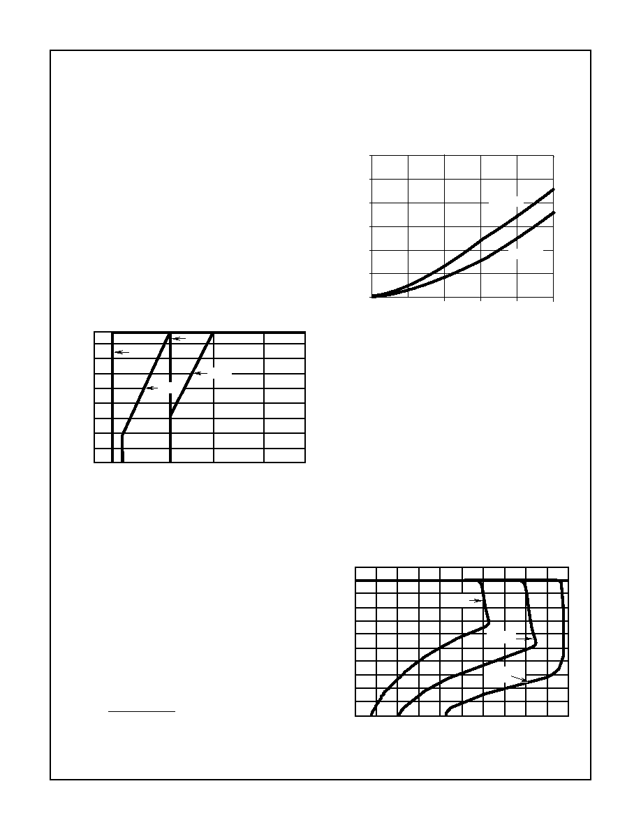
Determining the Power Dissipation in R1
Circuit efficiency is limited by the power dissipation in R1.
The power dissipation for 240Vrms and 120Vrms is shown in
Figure 5.
For input voltages other than 240Vrms or 120Vrms equation
10 can be used to determine the power dissipation in R1.
Example: R
1
= 100
, Input Voltage = 240Vrms, I
OUT
=
50mA, P
D
= 4.8W
Pd = 2.8
(EQ. 10)
275
240
210
180
150
120
90
60
30
0
INPUT VOL
T
AGE (V
rms)
0
75 100
220
330
470
10mA
35mA
25mA
C2 (
µ
F)
OFFLINE WORLD-WIDE SUPPLY
50mA
R1 Vrms (I
OUT
)
3
NOTE: Under short circuit conditions the P
D
in R1
decreases to 1.2W Due to fold back current limiting (I
OUT
=
20mA, Reference Figure 6).
FIGURE 5. POWER DISSIPATION IN R1 vs LOAD CURRENT
Operation Information
Effects of Temperature on Output Current:
Figure 6 shows the effects of temperature on the output
current for the circuit shown in Figure 1. Figure 6 illustrates
operation with the output configured for 5V. Temperature
effects on the output current for V
OUT
= 24V operation is
similar. The foldback current limiting is the result of reduced
voltage on C2. The circuit delivers 50mA output current
across the specified temperature range of -40
o
C to +85
o
C
for all output voltages between 5V and 24V. The effect of
decreasing the value of C2 (470
µ
F) reduces the maximum
output current (i.e. moves curve to the left). For all C2 values
selected from Figure 4 (assuming tolerance and temperature
coefficient are taken into account) the circuit meets the
expected output current across the above mentioned
temperature range.
FIGURE 6. OUTPUT CURRENT vs TEMPERATURE
LOAD CURRENT (mA)
POWER DISSIP
A
TION (W)
0
1
2
3
4
5
6
0
10
20
30
40
50
120Vrms
OFFLINE WORLD-WIDE SUPPLY (R1 = 100
)
240Vrms
5
4
3
2
1
0
10
20
30
40
50
60
70
80
90
100
OUTPUT CURRENT (mA)
OUTPUT VOL
T
AGE (V)
OFFLINE WORLD-WIDE SUPPLY
+85
o
C
+25
o
C
-40
o
C
Application Information
(Continued)