 | –≠–ª–µ–∫—Ç—Ä–æ–Ω–Ω—ã–π –∫–æ–º–ø–æ–Ω–µ–Ω—Ç: HTC750xSI | –°–∫–∞—á–∞—Ç—å:  PDF PDF  ZIP ZIP |

HIGH TECH
CHIPS, INC.
04/30/00 1
PDIP, SOIC
1
8
2
7
3
6
4
5
HTC750XXX
VDD GND
NU MOUT
NU CNTL
D1 D0
Melody Generator
1.0 General description.
This circuit is designed to work as melody generator. HTC750 will play selected melody (selection is
done by driving D0 and D1 inputs to low or high value) and once melody is finished it will enter power
saving mode which we call Sleep mode. In Sleep mode HTC750 consumes less then few microamps
of current. One of possible uses of HTC750 is designing it in doorbell. This device was designed
using our proprietary melody storing scheme to optimize
internal memory usage. HTC750 can play up to four melodies.
It can directly drive piezo-electrical sound source or with use of
external amplifier can drive speakers. Control output is
provided to control external relay or power switch. This output
goes high for duration of melody and could be used to control
the power to HTC750 and amplifier for duration of melody.
Possible uses are:
∑ Musical
doorbell.
∑ Melody generator for alarm clock.
∑ Musical
toys.
∑ Musical boxes for gifts, accessories or jewelry.
Features:
∑ Single chip solution.
∑ Minimum external components.
∑ Four
selectable
melodies.
∑ Minimum power consumption while in SLEEP mode.
Doorbell design using HTC750
C1
0.1uF
R3
1K
4.5V
BT1
Q1
NPN
Q2
PNP
LS1
8ohm
C3
47uF
1
2
4
3
R2
100K
R1
100K
U1
HTC750
NU
2
NU
3
MOUT
7
VDD
1
CNTL
6
D1
4
D0
5
GND
8
S1

HIGH TECH
CHIPS, INC.
04/30/00 2
2.0 Functional Description.
We will use schematics above to describe HTC750 operation. At power up HTC750 plays melody set
by dip-switch. After finishing melody it goes into sleep mode and drives all outputs to GND. In
prototypes we build using above schematics current consumption was less then 10uA. This current is
negligible enough to leave circuit constantly powered on. When device is in Sleep mode only way of
waking up the circuit is to recycle power. This is done using S1 pushbutton. Note that we are using
pushbutton with normal closed contacts. When this pushbutton is activated power to HTC750 is cut
down and when this pushbutton is released then part will play the melody. One can use pushbutton
with normal open contacts but it could result partial reproduction of melody.
Note the way CNTL output is used to save energy during Sleep mode. Energy saving is achieved by
cutting power to R1 and R2 resistors when part enters into Sleep mode and preventing battery
discharge through those resistors when associated dip-switch is on. T1 and T2 form simple current
amplifier to drive 8-ohm speaker. Almost any small signal transistor could be used in this amplifier.
Note that this amplifier will introduce additional distortions to amplified signal, because transistors are
not biased. This is done intentionally to simplify amplifier circuit and add one distinct character. This
amplifier does not use any current when its input is driven low. Any other amplifier circuit could be
used as long as care is taken to shut down the amplifier with CNTL output of HTC750 to save buttery.
This could be done by external relay. Quality of sound could be further enhanced if low pass filter is
added to output of HTC750. Please see Application note for HTC750.
Pin out description.
Abbreviations used: O - output, I - input, P - power.
Pin
Name
I / O Description
Notes
1
VDD
P
Power
+2.5V to +5.5V
2
NU
I
Not Used
Tie it to GND or VDD.
3
NU
I
Not Used
Tie it to GND or VDD.
4
D1
I
Melody selection input.
Tie it to GND or VDD.
5
D0
I
Melody selection input.
Tie it to GND or VDD.
6
CNTL
O
Control output
This output is driven high when part plays
melody. Can deliver up to 25mA current.
7
MOUT
O
Melody output
Signal on this output is square wave.
8
GND
P
Ground
Connect to ground.
3.0 Melody selection with D[0:1]
D1
D0
MELODY
GND
GND
Number 1
GND
VDD
Number 2
VDD
GND
Number 3
VDD
GND
Number 4

HIGH TECH
CHIPS, INC.
04/30/00 3
This table shows melody played when D0 and D1 are tied to ground or power. Note that this
part comes with different sets of melodies and those melody samples will be made available
for download.
4.0 Electrical characteristics.
Voltage on VDD pin in respect to GND
+2.5 to +5.5V
Operational current with no external load
3 mA
1
Current used in SLEEP mode
4uA
1
MOUT
output low voltage max (5mA load)
0.4V
1
MOUT
output high voltage min (5mA source)
VDD-0.7V
1
MOUT
maximum sink current
25mA
1
MOUT
maximum source current
25mA
1
CNTL
output low voltage max (5mA load)
0.4V
1
CNTL
output high voltage min (5mA source)
VDD-0.7V
1
CNTL
maximum sink current
25mA
1
CNTL
maximum source current
25mA
1
NOTES:
1. Those values are characterized but not tested.
5.0 Ordering information.
H
T
C
7
5
0
X
X
X
OPTIONAL: Temperature range:
C = 0
o
C to +70
o
C , I = - 40
o
C to + 85
o
C.
PACKAGE:
S ≠ 208 mil SOIC
D ≠ 300 mil PDIP.
MELODY
PART NUMBER.

HIGH TECH
CHIPS, INC.
04/30/00 4
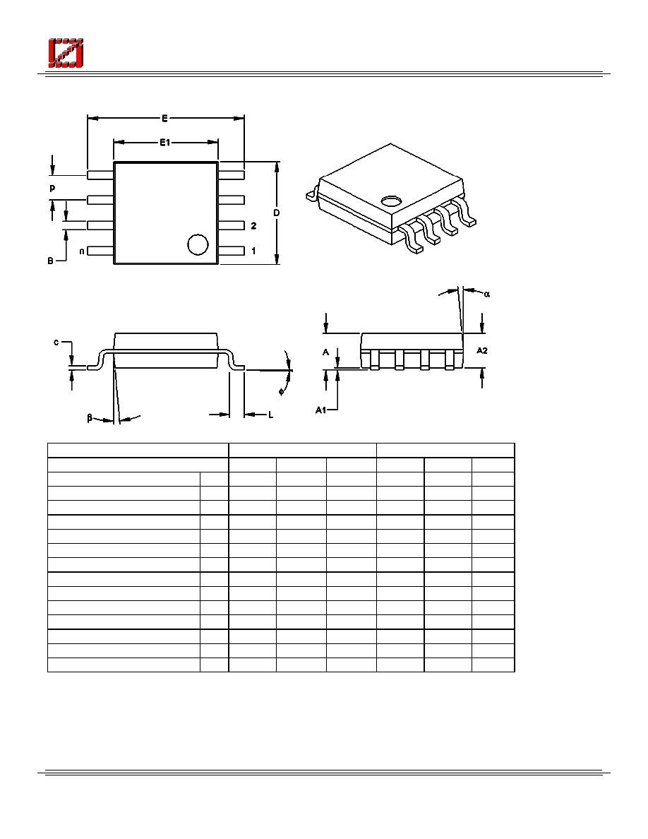
6.0 Mechanical information.
8-Lead Plastic Dual In-line (P) ≠ 300 mil (PDIP)
Units
INCHES*
MILLIMETERS
Dimension Limits
MIN
NOM
MAX
MIN
NOM
MAX
Number of Pins
n
8
8
Pitch
p
.100
2.54
Top to Seating Plane
A
.140
.155
.170
3.56
3.94
4.32
Molded Package Thickness
A2
.115
.130
.145
2.92
3.30
3.68
Base to Seating Plane
A1
.015
0.38
Shoulder to Shoulder Width
E
.300
.313
.325
7.62
7.94
8.26
Molded Package Width
E1
.240
.250
.260
6.10
6.35
6.60
Overall Length
D
.360
.373
.385
9.14
9.46
9.78
Tip to Seating Plane
L
.125
.130
.135
3.18
3.30
3.43
Lead Thickness
c
.008
.012
.015
0.20
0.29
0.38
Upper Lead Width
B1
.045
.058
.070
1.14
1.46
1.78
Lower Lead Width
B
.014
.018
.022
0.36
0.46
0.56
Overall Row Spacing
eB
.310
.370
.430
7.87
9.40
10.92
Mold Draft Angle Top
5
10
15
5
10
15
Mold Draft Angle Bottom
5
10
15
5
10
15
*Controlling Parameter
Notes:
Dimensions D and E1 do not include mold flash protrusions. Mold flash or protrusions shell
not exceed .010" (0.254mm)per side.
JEDEC Equivalent:MS-001
HIGH TECH
CHIPS, INC.
04/30/00 5
8-Lead Plastic Small Outline (SM) ≠ Medium, 208 mil (SOIC)
Units
INCHES
*
MILLIMETERS
Dimension Limits
MIN
NOM
MAX
MIN
NOM
MAX
Number of Pins
n
8
8
Pitch
P
.050
1.27
Overall Height
A
.070
.075
.080
1.78
1.97
2.03
Molded Package Thickness
A2
.069
.074
.078
1.75
1.88
1.98
Standoff
A1
.002
.005
.010
0.05
0.13
0.25
Overall Width
E
.300
.313
.325
7.62
7.95
8.26
Molded Package Width
E1
.201
.208
.212
5.11
5.28
5.38
Overall Length
D
.202
.205
.210
5.13
5.21
5.33
Foot Length
L
.020
.025
.030
0.51
0.64
0.76
Foot Angle
0
4
8
0
4
8
Lead Thickness
c
.008
.009
.010
0.20
0.23
0.25
Lead Width
B
.014
.017
.020
0.36
0.43
0.51
Mold Draft Angle Top
0
12
15
0
12
15
Mold Draft Angle Bottom
0 12
15
0
12
15
*Controlling Parameter
Notes:
Dimensions D and E1 do not include mold flash protrusions. Mold flash or
protrusions shell not exceed .010" (0.254mm)per side.