 | –≠–ª–µ–∫—Ç—Ä–æ–Ω–Ω—ã–π –∫–æ–º–ø–æ–Ω–µ–Ω—Ç: 2SD1418 | –°–∫–∞—á–∞—Ç—å:  PDF PDF  ZIP ZIP |
2SD1418
Silicon NPN Epitaxial
Application
∑
Low frequency power amplifier
∑
Complementary pair with 2SB1025
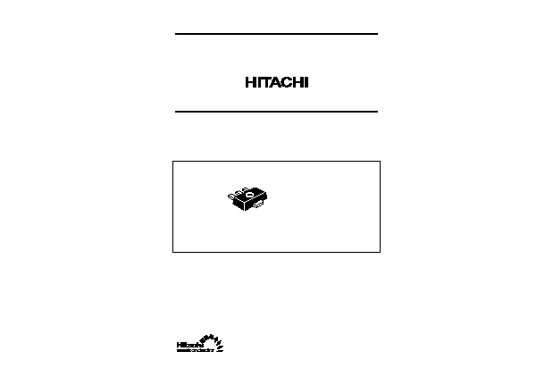
Outline
UPAK
1. Base
2. Collector
3. Emitter
4. Collector (Flange)
4
1
2
3
2SD1418
2
Absolute Maximum Ratings (Ta = 25∞C)
Item
Symbol
Ratings
Unit
Collector to base voltage
V
CBO
120
V
Collector to emitter voltage
V
CEO
80
V
Emitter to base voltage
V
EBO
5
V
Collector current
I
C
1
A
Collector peak current
i
C(peak)
*
1
2
A
Collector power dissipation
P
C
*
2
1
W
Junction temperature
Tj
150
∞
C
Storage temperature
Tstg
≠55 to +150
∞
C
Notes: 1. PW
10 ms, Duty cycle
20%
2. Value on the alumina ceramic board (12.5 x 20 x 0.7 mm)
Electrical Characteristics (Ta = 25∞C)
Item
Symbol
Min
Typ
Max
Unit
Test conditions
Collector to base breakdown
voltage
V
(BR)CBO
120
--
--
V
I
C
= 10
µ
A, I
E
= 0
Collector to emitter breakdown
voltage
V
(BR)CEO
80
--
--
V
I
C
= 1 mA, R
BE
=
Emitter to base breakdown
voltage
V
(BR)EBO
5
--
--
V
I
E
= 10
µ
A, I
C
= 0
Collector cutoff current
I
CBO
--
--
10
µ
A
V
CB
= 100 V, I
E
= 0
DC current transfer ratio
h
FE1
*
1
60
--
320
V
EB
= 5 V, I
C
= 150 mA*
2
h
FE2
30
--
--
V
CE
= 5 V, I
C
= 500 mA*
2
Collector to emitter saturation
voltage
V
CE(sat)
--
--
1
V
I
C
= 500 mA, I
B
= 50 mA*
2
Base to emitter voltage
V
BE
--
--
1.5
V
V
CE
= 5 V, I
C
= 150 mA*
2
Gain bandwidth product
f
T
--
140
--
MHz
V
CE
= 5 V, I
C
= 150 mA*
2
Collector output capacitance
Cob
--
12
--
pF
V
CB
= 10 V, I
E
= 0, f = 1 MHz
Notes: 1. The 2SD1418 is grouped by h
FE1
as follows.
2. Pulse test
Mark
DA
DB
DC
h
FE1
60 to 120
100 to 200
160 to 320

2SD1418
3
150
100
50
Ambient Temperature Ta (
∞
C)
0
1.2
0.8
0.4
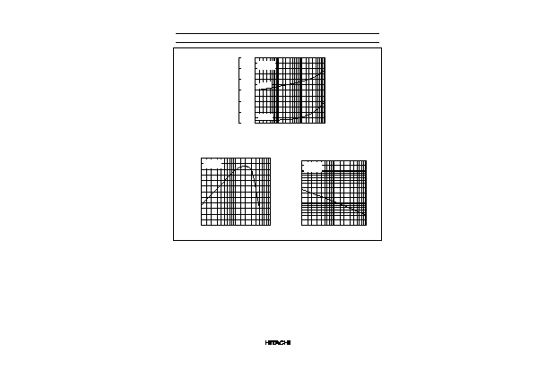
Maximum Collector Dissipation Curve
Collector Power Dissipation P
C
(W)
(on the alumina ceramic board)
8
4
10
6
2
Collector to Emitter Voltage V
CE
(V)
0
1.0
0.8
0.6
0.4
0.2
Typical Output Characteristics
Collector Current I
C
(A)
I
B
= 0
1
2
5
10
15
20
25
30
35
0.5 mA
0
0.4
0.8
0.2
0.6
1.0
Base to Emitter Voltage V
BE
(V)
500
200
100
50
20
5
2
1
10
Typical Transfer Characteristics
Collector Current I
C
(mA)
V
CE
= 5 V
Ta = 75
∞
C
25
≠25
10
100
1,000
30
300
3
1
Collector Current I
C
(mA)
300
250
200
150
100
50
0
DC Current Transfer Ratio h
FE
DC Current Transfer Ratio vs. Collector Current
V
CE
= 5 V
Ta = 75
∞
C
25
≠25
2SD1418
4
10
100
1,000
30
300
3
1
Collector Current I
C
(mA)
1.2
1.0
0.8
0.6
0.4
0.2
0
0.6
0.5
0.4
0.3
0.2
0.1
0
Base to Emitter Saturation Voltage V
BE(sat)
(V)
Collector to Emitter Saturation Voltage V
CE(sat)
(V)
Saturation Voltage vs. Collector Current
I
C
= 10 I
B
Pulse
V
CE(sat)
V
BE(sat)
10
30
100
300
1,000
Collector Current I
C
(mA)
240
200
160
120
80
40
0
Gain Bandwidth Product vs. Collector Current
Gain Bandwidth Product f
T
(MHz)
V
CE
= 5 V
Pulse
2
50
10
5
20
100
1
Collector to Base Voltage V
CB
(V)
200
10
100
50
20
5
2
Collector Output Capacitance C
ob
(pF)
Collector Output Capacitance vs.
Collector to Base Voltage
f = 1 MHz
I
E
= 0

4.5
±
0.1
1.8 Max
1.5
±
0.1
0.44 Max
0.44 Max
0.48 Max
0.53 Max
1.5 1.5
3.0
2.5
±
0.1
4.25 Max
0.8 Min
1
0.4
(1.5)
(2.5)
(0.4)
(0.2)
Hitachi Code
JEDEC
EIAJ
Weight (reference value)
UPAK
--
Conforms
0.050 g
Unit: mm