HD74HC590
8-bit Binary Counter/Register (with 3-state outputs)
Description
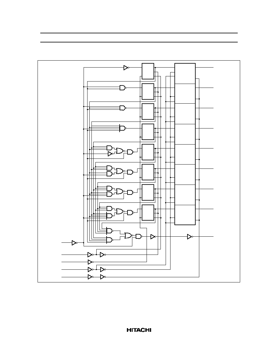
This device each contains an 8-bit binary counter that feeds an 8-bit storage register. The storage register
has parallel outputs. Separate clocks are provided for both the binary counter and storage register. The
binary counter features a direct clear input
CCLR and a count enable input C CKEN. For cascading a ripple
carry output
R CO is provided. Expansion is easily accomplished by tying R CO of the first stage to CCKEN
of the second stage, etc.
Both the counter and register clocks are positive-edge triggered. If the user wishes to connect both clocks
together, the counter state will always be one count ahead of the register, Internal circuitry prevents
clocking from the clock enable.
Features
∑
High Speed Operation: t
pd
(RCK to Q) = 18.5 ns typ (C
L
= 50 pF)
∑
High Output Current: Fanout of 15 LSTTL Loads
∑
Wide Operating Voltage: V
CC
= 2 to 6 V
∑
Low Input Current: 1 µA max
∑
Low Quiescent Supply Current: I
CC
(static) = 4 µA max (Ta = 25∞C)
HD74HC590
2
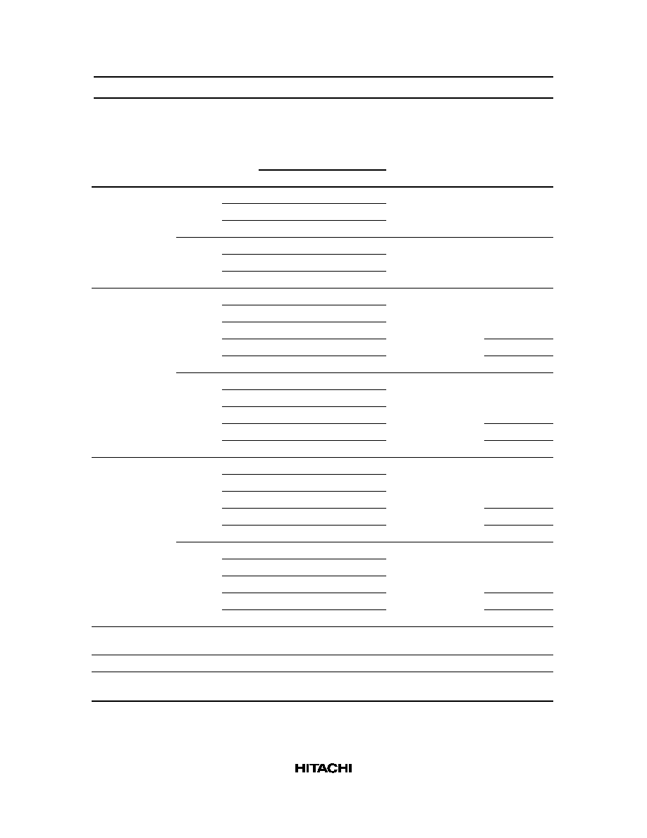
Function Table
Inputs
G
RCK
CCLR
CCKEN
CCK
Function
H
X
X
X
X
Q output disabled
L
X
X
X
X
Q output enabled
X
X
X
X
Contents of counter stored to register
X
X
X
X
No change in register
X
X
L
X
X
Counter clear
X
X
H
L
Count up
X
X
H
L
No count
X
X
H
H
X
No count
RCO = QA'∑QB'∑QC'∑QD'∑QE'∑QF'∑QG'∑QH'∑ (CCKEN) (QA' to QH': Output of Internal Counter)
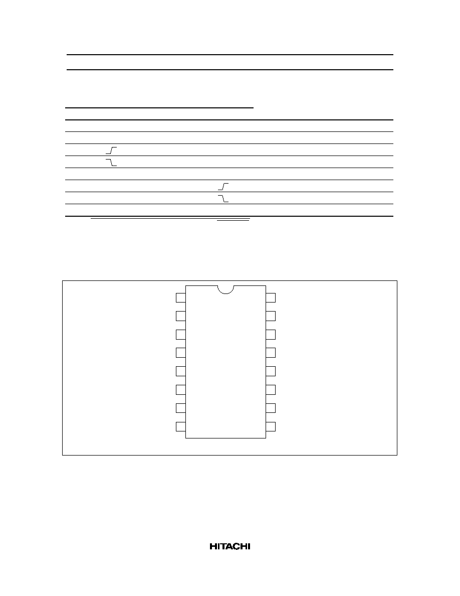
Pin Arrangement
1
(Top view)
2
3
4
5
6
7
8
9
10
11
12
13
14
15
16
Q
B
V
CC
Q
A
C
CCKEN
CCK
CCLR
RCO
RCK
Q
C
Q
D
Q
E
Q
F
Q
G
Q
H
GND