
HD26LS32A
Quadruple Differential Line Receivers With 3 State Outputs
The HD26LS32A features quadruple line receivers
designed to meet the specs of EIA standard RS-
422A and RS-423. This device operates from a
single 5 V power supply. The enable function is
common to all four receivers and offers a choice
of active high or active low input. Fail safe design
ensures that if the inputs are open, the outputs will
always be high.
Logic Diagram
Function Table
Pin Arrangement
Enable
G
V
ID
V
TL
H
X
H
X
H
X
Output
Y
G
X
L
X
L
X
L
?
L
V
ID
V
TH
X
V
TL
< V
ID
< V
TH
Differential Input
A ≠ B
High level
Low level
Immaterial
Irrelevant
High impedance
H
L
X
?
Z
:
:
:
:
:
H
H
?
L
L
H
Z
1A
1B
2A
2B
3A
3B
4A
4B
1Y
2Y
3Y
4Y
Enable G
Enable G
(Top View)
V
CC
1
2
3
4
5
6
7
8
1B
9
10
11
12
13
14
15
16
Enable
G
1A
1Y
2Y
2A
2B
GND
4B
4A
4Y
3Y
3A
3B
Enable
G
2
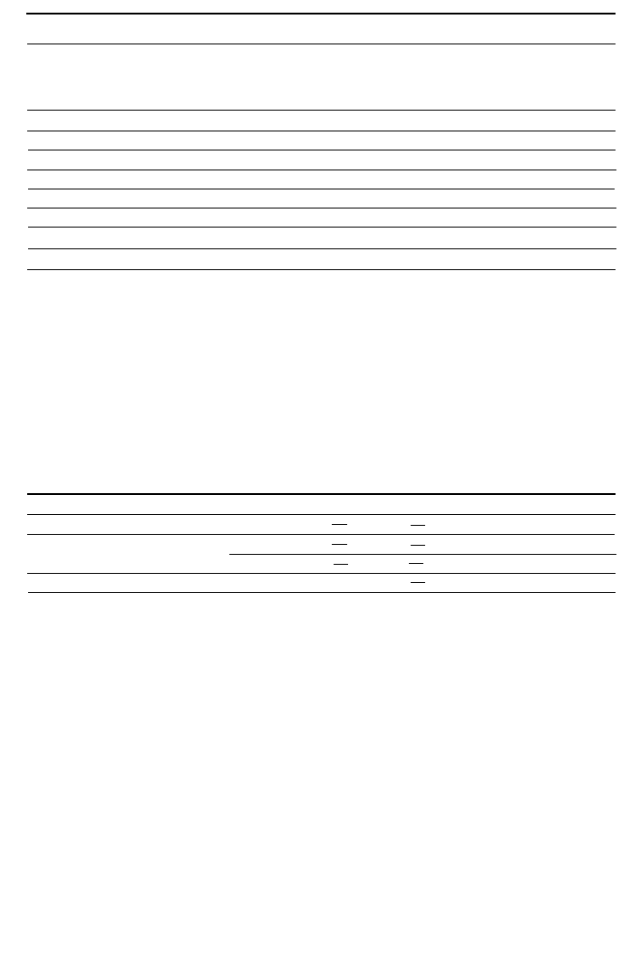
Absolute Maximum Ratings
HD26LS32A
Notes: 1. All voltage values except for differential input voltage are with respect to network ground
terminal.
2. Differential input voltage is measured at the noninverting input with respect to the
corresponding inverting input.
3. The absolute maximum ratings are values which must not individually be exceeded, and
furthermore, no two of which may be realized at the same time.
Unit
Recommended Operating Conditions
Item
Supply Voltage
Differential Input Voltage
Storage Temperature
V
V
V
mA
∞
C
Output Sink Current
V
Enable Input Voltage
Input Voltage A or B
Continuous Total Dissipation
Operating Temperature
Symbol
V
CC
V
IN
V
ID
V
IN
T
stg
I
out
*2
*1
T
opr
P
T
Ratings
≠ 65 to 150
±
25
7.0
±
25
7
0 to +70
1
50
∞
C
W
Item
Symbol
Supply Voltage
In Phase Input Voltage
V
CC
V
IC
I
OH
Unit
V
V
µ
A
∞
C
Min
Typ
Max
4.75
0
5.00
5.25
Operating Temperature
I
OL
Output Current
T
opr
±
7.0
≠ 440
8
70
mA
HD26LS32A

HD26LS32A
3
Electrical Characteristics (Ta = 0 to +70
∞
C)
Item
Symbol
Min
Typ
Max
Unit
Conditions
Differential Input High
Threshold Voltage
V
TH
V
TL
V
TH
≠V
TL
V
IH
V
OH
Input Hysteresis
Enable Input Voltage
V
IL
I
OZ
Input Resistance
Differential Input Low
Threshold Voltage
V
IC
=
≠7 to +7 V
V
OH
= 2.7V, I
OH
= ≠440
µ
A
V
OL
= 0.4 V, I
OL
= 4 mA
V
OL
= 0.45 V, I
OL
= 8 mA
0.2
V
*1
≠0.2
≠0.2
50
Enable Input
Clamp Voltage
Output Voltage
V
IK
V
OL
Off State(High Impedance)
Output Current
Line Input Current
Enable Input Current
Short Circuit
Output Current
Supply Current
I
I
I
I (EN)
I
IH
I
IL
r
i
I
OS
I
CC
*3
V
CC
= 5.25V, V
I
= 0V
(All Outputs Disable)
mV
V
CC
= 4.75 V, I
IN
= ≠18 mA
V
CC
= 4.75V,
V
IL
(G)
= 0.8V
V
ID
= 1V, I
OH
= ≠440
µ
A
V
ID
= ≠1 V, I
OL
= 4 mA
V
ID
= ≠1 V, I
OL
= 8 mA
V
CC
= 5.25V
V
O
= 2.4 V
V
O
= 0.4 V
V
I
= 15 V, Other Inputs≠10 to +15 V
V
I
= ≠15 V, Other Inputs≠15 to +10 V
V
I
= 5.5 V
V
I
= 2.7 V
V
I
= 0.4 V
V
IC
= ≠15 to +15 V
(Other Inputs AC GND)
V
CC
= 5.25 V
2.0
0.8
≠1.5
2.7
0.4
0.45
20
≠20
2.3
≠2.8
100
20
≠0.36
9.8
6
≠15
≠85
70
52
V
µ
A
mA
µ
A
mA
K
mA
Notes: 1. All typical values are at V
CC
=5V, Ta=25
∞
C,V
IC
=0.
2. Hysteresis is the differential between the positive going input threshold voltage and the
negative going input threshold voltage.
3. Not more than one output should be shorted at a time.
*2
HD26LS32A

5
HD26LS32A
2. t
HZ
, t
ZH
1.3 V
1.3 V
1.3 V
1.3 V
Enable G
3 V
0 V
3 V
0 V
1.3 V
1.4 V
0V
0.5 V
t
ZH
t
HZ
Pulse
Generator
Input
2 V
2.5 V
Test circuit
Waveforms
Output
C
L
5 K
V
CC
S
1
2 K
Enable G
Output
S
1
:Open
S
1
:Closed
3. t
LZ
, t
ZL
H
Notes: 1. The pulse generator has the following characteristics :
PRR=1 MH
Z
, 50 % duty cycle, t
r
6ns, t
f
6ns, Zout=50
.
2. C
L
includes probe and jig capacitance.
3. All diodes are 1S2074
4. To test G input,ground G input and apply an inverted
input waveform.
1.3 V
1.3 V
1.3 V
1.3 V
Enable G
1.4 V
Pulse
Generator
Input
2 V
≠2.5 V
Test circuit
Waveforms
Output
C
L
5 K
V
CC
2 K
Enable G
Output
S
2
:Open
1.3 V
0.5 V
t
LZ
S
2
:Closed
S
2
t
ZL
V
OL
3 V
0 V
3 V
0 V
HD26LS32A
