 | –≠–ª–µ–∫—Ç—Ä–æ–Ω–Ω—ã–π –∫–æ–º–ø–æ–Ω–µ–Ω—Ç: HD29051P | –°–∫–∞—á–∞—Ç—å:  PDF PDF  ZIP ZIP |
Rev.3.00, Jul.16.2004, page 1 of 10
HD29051
Dual Differential Line Drivers/ReceiversWith 3 State Outputs
REJ03D0305≠0300Z
(Previous ADE-205-035A (Z))
Rev.3.00
Jul.16.2004
Description
The HD29051 features differential line drivers/receivers with three state output designed to meet the spec of EIA RS-
422A and 423A. Each device has two drivers/receivers in a 16 pin package.
The device becomes in enable state when active high for a driver and active low for a receiver.
Features
Driver
∑
Built in current restriction when short circuit
∑
Power up/down protection.
∑
High output current
I
OH
= ≠40 mA
I
OL
= 40 mA
Receiver
∑
Input hysteresis (Typ. 50 mV)
∑
In phase input voltage ±200 mV of input sensitivity in the range ≠7 to +12 V.
∑
Ordering Information
Part Name
Package Type
Package Code
Package
Abbreviation
Taping Abbreviation
(Quantity)
HD29051P
DILP-16 pin
DP-16E, -16FV
P
--
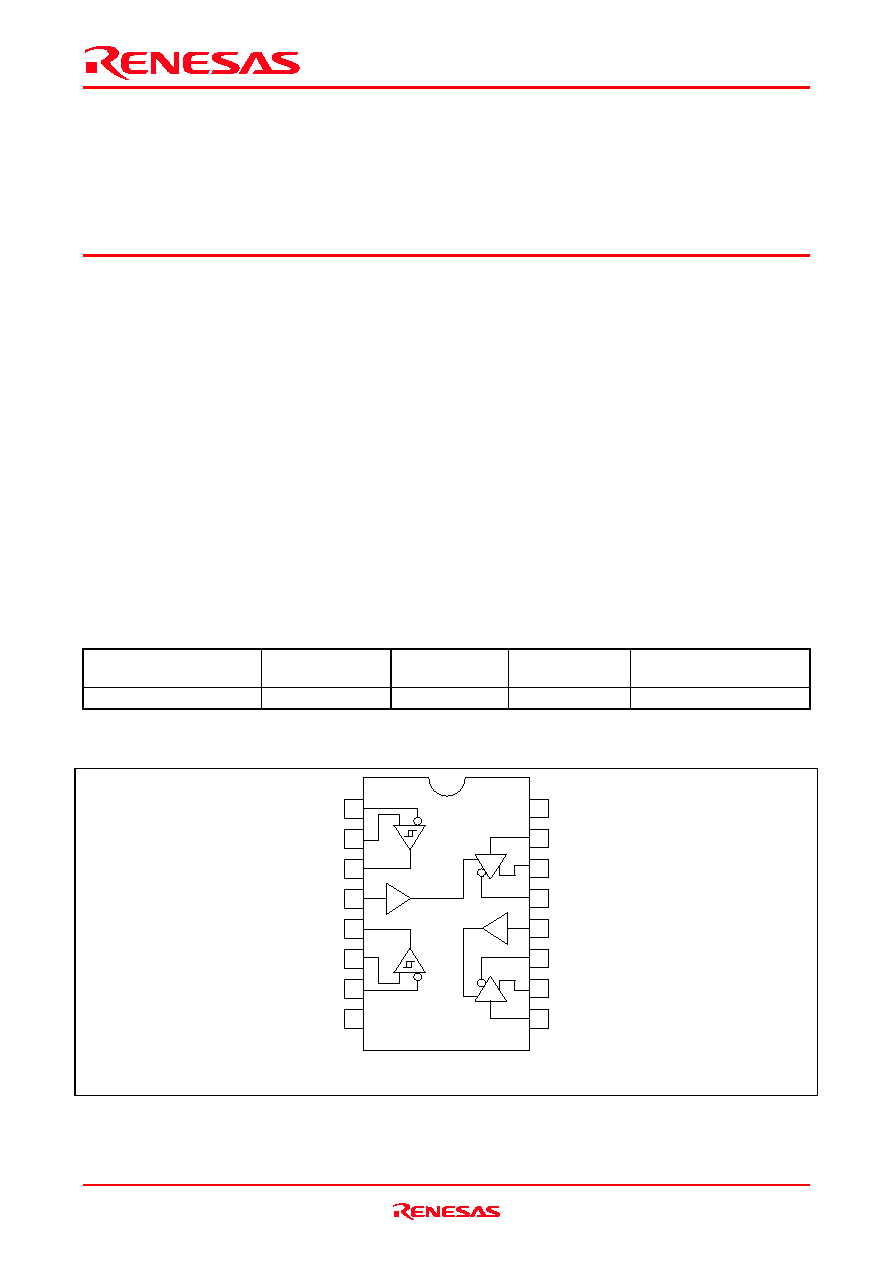
Pin Arrangement
(Top view)
1
2
3
4
5
6
7
R1B
GND
R1A
R1Y
R2Y
8
D1 Enable
R2A
R2B
13
14
15
10
11
12
9
16 V
CC
D1A
D1Y
D1Z
D2 Enable
D2Z
D2Y
D2A
HD29051
Rev.3.00, Jul.16.2004, page 2 of 10
Function Table
Drivers
Receivers
Input A
Enable
Output Y
Output Z
Differential Input A ≠ B
Output Y
L
H
L
H
V
ID
0.2 V
H
H
H
H
L
≠0.2 V < V
ID
< 0.2 V
?
X
L
Z
Z
V
ID
≠0.2 V
L
H :
High level
L :
Low level
Z :
High impedance
X :
Immaterial
? :
Irrelevant
Absolute Maximum Ratings
Item
Symbol
Ratings
Unit
Supply Voltage*
1
V
CC
7
V
Input Voltage A, B*
3
V
IN
±25
V
Differential Input Voltage*
2
*
3
V
ID
±25
V
Output Current*
3
I
O
50
mA
Enable Input Voltage
V
IE
5.5
V
Input Voltage*
4
V
IN
5.5
V
Output Applied Voltage*
4
*
5
V
O
≠1.0 to 7.0
V
Operating Temperature Range
Topr
0 to 70
∞C
Storage Temperature Range
Tstg
≠65 to 150
∞C
Notes: 1. All voltage values except for differential input voltage are with respect to network ground terminal.
2. Differential input voltage is measured at the noninverting input with respect to the corresponding inverting
input.
3. Only receiver
4. Only driver
5. Z state
6. The absolute maximum ratings are values which must not individually be exceeded, and furthermore, no two
of which may be realized at the same time.
Recommended Operating Conditions
Item
Symbol
Min
Typ
Max
Unit
Supply Voltage
V
CC
4.75
5.0
5.25
V
In Phase Input Voltage*
1
V
IC
≠7.0
--
12
V
Differential Input Voltage*
1
V
ID
≠6.0
--
6.0
V
Enable Input Voltage
V
IE
0
--
5.25
V
Input Voltage*
2
V
IN
0
--
5.25
V
Operating Temperature
Topr
0
25
70
∞C
Notes: 1. Only receiver
2. Only driver

HD29051
Rev.3.00, Jul.16.2004, page 3 of 10
Electrical Characteristics
(Ta = 0 to +70∞C)
Driver
Item
Symbol
Min
Typ
Max
Unit
Conditions
Input Voltage
V
IHD
2.0
--
--
V
V
ILD
--
--
0.8
V
Input Clamp Voltage
V
IKD
--
--
≠1.5
V
V
CC
= 4.75 V, I
I
= ≠18 mA
Output Voltage
V
OHD
2.5
--
--
V
V
CC
= 4.75 V, I
OH
= ≠20 mA
2.4
--
--
V
V
CC
= 4.75 V, I
OH
= ≠40 mA
V
OLD
--
--
0.45
V
V
CC
= 4.75 V, I
OL
= 20 mA
--
--
0.5
V
V
CC
= 4.75 V, I
OL
= 40 mA
Output Leak Current
I
OZD
≠100
--
100
µA
V
CC
= 5.25 V, V
O
= 0.5 V
Enable = 0.8 V
≠100
--
100
µA
V
CC
= 5.25 V, V
O
= 2.7 V
Enable = 0.8 V
I
O(Off)
--
--
≠100
µA
V
CC
= 0 V, V
O
= ≠0.25 V
--
--
100
µA
V
CC
= 0 V, V
O
= 6.0 V
Input Current
I
ID
--
--
100
µA
V
CC
= 5.25 V, V
I
= 5.25 V
I
IHD
--
--
20
µA
V
CC
= 5.25 V, V
I
= 2.7 V
I
ILD
--
--
≠360
µA
V
CC
= 5.25 V, V
I
= 0.4 V
Differential Output Voltage
|V
OC
|
--
--
0.4
V
|V
OD2
|
2.0
--
--
V
|V
OD
|
--
--
0.4
V
Short Circuit Output
Current*
1
I
OSD
≠30
--
≠150
mA
V
CC
= 5.25 V, V
O
= 0 V
Electrical Characteristics
(Ta = 0 to +70∞C)
Receiver
Item
Symbol
Min
Typ
Max
Unit
Conditions
Differential Input Threshold V
THR
--
--
0.2
V
V
O
2.7 V ≠7.0 V < V
IC
< 12 V
Voltage*
2
≠0.2
--
--
V
V
O
0.45 V, ≠7.0 V < V
IC
< 12 V
Input Current
I
IBR
--
--
1.0
mA
V
IN
= 12 V, 0 V
V
CC
5.25 V
--
--
≠0.8
mA
V
IN
= ≠7 V, 0 V
V
CC
5.25 V
Output Voltage
V
OHR
2.7
--
--
V
V
CC
= 4.75 V, I
O
= ≠400 mA
V
ID
= 0.4 V, ≠7.0 V < V
IC
< 12 V
V
OLR
--
--
0.45
V
V
CC
= 4.75 V, I
O
= 8.0 mA
V
ID
= ≠0.4 V, ≠7.0 V < V
IC
< 12 V
Short Circuit Output
Current*
1
I
OSR
≠15
--
≠85
mA
V
CC
= 5.25 V, V
O
= 0 V V
ID
= 3.0 V
Supply
Item
Symbol
Min
Typ
Max
Unit
Conditions
Supply Current
I
CC
--
55*
3
80
mA
V
CC
= 5.25 V
Notes: 1. Not more than one output should be shorted at a time, and duration of the short circuit should not exceed one
second.
2. In this table, only the threshold voltage is expressed in algebra.
3. All typical values are at V
CC
= 5V, Ta = 25∞C.
HD29051
Rev.3.00, Jul.16.2004, page 4 of 10
Switching Characteristics (Ta = 25∞C, V
CC
= 5 V)
Driver
Item Symbol
Min
Typ
Max
Unit
Conditions
Propagation Delay Time
t
PLHD
--
-- 20 ns
C
L
= 30 pF, R
L
= 75
to GND
R
L
= 180
to V
CC
t
PHLD
--
-- 20 ns
C
L
= 30 pF, R
L
= 75
to GND
R
L
= 180
to V
CC
Propagation Delay Time
Difference
t
SKD
*
1
--
-- 4 ns
C
L
= 30 pF, R
L
= 75
to GND
R
L
= 180
to V
CC
Output Enable Time
t
ZHD
--
-- 20 ns
C
L
= 30 pF, R
L
= 75
to GND
t
ZLD
--
-- 35 ns
C
L
= 30 pF, R
L
= 180
to V
CC
Output Disable Time
t
HZD
--
-- 20 ns
C
L
= 10 pF, R
L
= 75
to GND
t
LZD
--
-- 25 ns
C
L
= 10 pF, R
L
= 180
to V
CC
Receiver
Item Symbol
Min
Typ
Max
Unit
Conditions
Propagation Delay Time
t
PLHR
--
-- 40 ns
C
L
= 15 pF
t
PHLR
--
-- 40 ns
C
L
= 15 pF
Note: 1.
t
SKD
= |t
PLHD
≠ t
PHLD
|
DC Test (|V
OD2
|,
|V
OD
|, V
OC
,
|V
OC
|)
|V
OD2
|,
|V
OD
| Test
Y
Z
50
50
V 2
OD
V
OC
,
|V
OC
| Test
Y
Z
50
50
R
V
OC
Note:
|V
OD
| and
|V
OC
| indicate the differences of voltage from the former states when Y and Z outputs
are inversed.
|V
OD
| = ||V
OD2
| ≠ |V
OD2
||
|V
OC
| = |V
OC
≠ V
OC
|
HD29051
Rev.3.00, Jul.16.2004, page 5 of 10
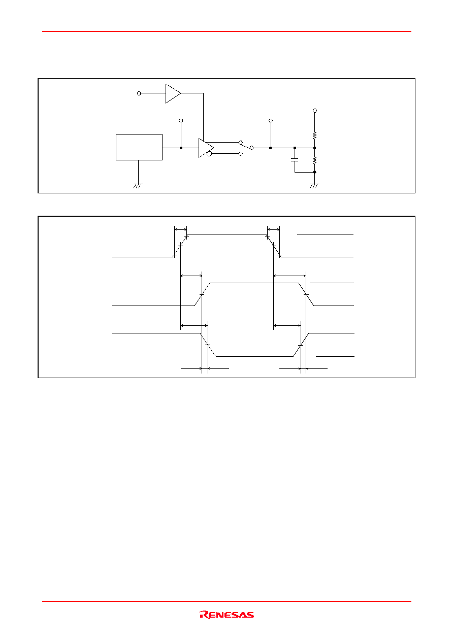
1. t
PLHD
, t
PHLD
Test circuit
Input
A
Y
Z
Output
R =
180
L
R =
75
L
5 V
C =
30 pF
L
Enable
3 V
Pulse
Generator
*1
*2
Waveforms
Input A
10 %
90 %
t
r
t
f
1.3 V
90 %
0 V
3 V
1.3 V
10 %
Output Y
t
PHLD
t
PLHD
t
PLHD
t
PHLD
1.3 V
1.3 V
OH
V
OL
V
1.3 V
1.3 V
V
OH
V
OL
Output Z
t
SKD
t
SKD