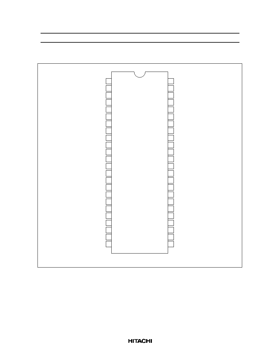
HD74ALVCH16244
16-bit Buffers / Drivers with 3-state Outputs
ADE-205-133C (Z)
4th. Edition
December 1999
Description
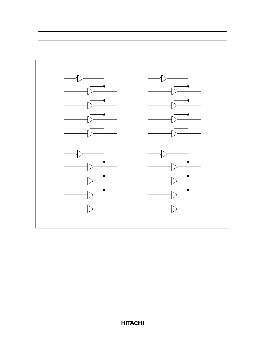
The HD74ALVCH16244 is designed specifically to improve both the performance and density of three
state memory address drivers, clock drivers, and bus oriented receivers and transmitters. The device can be
used as four 4-bit buffers, two 8-bit buffers, or one 16-bit buffer. It provides true outputs and symmetrical
OE (active-low output-enable) inputs. Active bus hold circuitry is provided to hold unused or floating data
inputs at a valid logic level.
Features
∑
V
CC
= 2.3 V to 3.6 V
∑
Typical V
OL
ground bounce < 0.8 V (@V
CC
= 3.3 V, Ta = 25
∞
C)
∑
Typical V
OH
undershoot > 2.0 V (@V
CC
= 3.3 V, Ta = 25
∞
C)
∑
Bus hold on data inputs eliminates the need for external pullup / pulldown resistors
Function Table
Inputs
Output Y
OE
A
L
H
H
L
L
L
H
X
Z
H : High level
L : Low level
X : Immaterial
Z : High impedance

HD74ALVCH16244
3
Absolute Maximum Ratings
Item
Symbol
Ratings
Unit
Conditions
Supply voltage
V
CC
≠0.5 to 4.6
V
Input voltage
*1
V
I
≠0.5 to 4.6
V
Output voltage
*1, 2
V
O
≠0.5 to V
CC
+0.5
V
Input clamp current
I
IK
≠50
mA
V
I
< 0
Output clamp current
I
OK
±
50
mA
V
O
< 0 or V
O
> V
CC
Continuous output current
I
O
±
50
mA
V
O
= 0 to V
CC
V
CC
, GND current / pin
I
CC
or I
GND
±
100
mA
Maximum power dissipation
at Ta = 55
∞
C (in still air)
*3
P
T
0.85
W
TSSOP
Storage temperature
Tstg
≠65 to 150
∞
C
Notes:
Stresses beyond those listed under "absolute maximum ratings" may cause permanent damage
to the device. These are stress ratings only, and functional operation of the device at these or
any other conditions beyond those indicated under "recommended operating conditions" is not
implied. Exposure to absolute maximum rated conditions for extended periods may affect device
reliability.
1. The input and output negative voltage ratings may be exceeded if the input and output clamp
current ratings are observed.
2. This value is limited to 4.6 V maximum.
3. The maximum package power dissipation is calculated using a junction temperature of 150
∞
C
and a board trace length of 750 mils.
Recommended Operating Conditions
Item
Symbol
Min
Max
Unit
Conditions
Supply voltage
V
CC
2.3
3.6
V
Input voltage
V
I
0
V
CC
V
Output voltage
V
O
0
V
CC
V
High level output current
I
OH
--
≠12
mA
V
CC
= 2.3 V
--
≠12
V
CC
= 2.7 V
--
≠24
V
CC
= 3.0 V
Low level output current
I
OL
--
12
mA
V
CC
= 2.3 V
--
12
V
CC
= 2.7 V
--
24
V
CC
= 3.0 V
Input transition rise or fall rate
t /
v
0
10
ns / V
Operating temperature
Ta
≠40
85
∞
C
Note:
Unused control inputs must be held high or low to prevent them from floating.

HD74ALVCH16244
5
Electrical Characteristics (Ta = ≠40 to 85
∞
C)
Item
Symbol V
CC
(V)
*1
Min
Max
Unit
Test Conditions
Input voltage
V
IH
2.3 to 2.7
1.7
--
V
2.7 to 3.6
2.0
--
V
IL
2.3 to 2.7
--
0.7
2.7 to 3.6
--
0.8
Output voltage
V
OH
Min to Max V
CC
≠0.2
--
V
I
OH
= ≠100
µ
A
2.3
2.0
--
I
OH
= ≠6 mA, V
IH
= 1.7 V
2.3
1.7
--
I
OH
= ≠12 mA, V
IH
= 1.7 V
2.7
2.2
--
I
OH
= ≠12 mA, V
IH
= 2.0 V
3.0
2.4
--
I
OH
= ≠12 mA, V
IH
= 2.0 V
3.0
2.0
--
I
OH
= ≠24 mA, V
IH
= 2.0 V
V
OL
Min to Max --
0.2
I
OL
= 100
µ
A
2.3
--
0.4
I
OL
= 6 mA, V
IL
= 0.7 V
2.3
--
0.7
I
OL
= 12 mA, V
IL
= 0.7 V
2.7
--
0.4
I
OL
= 12 mA, V
IL
= 0.8 V
3.0
--
0.55
I
OL
= 24 mA, V
IL
= 0.8 V
Input current
I
IN
3.6
--
±
5
µ
A
V
IN
= V
CC
or GND
I
IN (hold)
2.3
45
--
V
IN
= 0.7 V
2.3
≠45
--
V
IN
= 1.7 V
3.0
75
--
V
IN
= 0.8 V
3.0
≠75
--
V
IN
= 2.0 V
3.6
--
±
500
V
IN
= 0 to 3.6 V
Off state output current
*2
I
OZ
3.6
--
±
10
µ
A
V
OUT
= V
CC
or GND
Quiescent supply current I
CC
3.6
--
40
µ
A
V
IN
= V
CC
or GND
I
CC
3.0 to 3.6
--
750
µ
A
V
IN
= one input at (V
CC
≠0.6)
V,
other inputs at V
CC
or GND
Notes: 1. For conditions shown as Min or Max, use the appropriate values under recommended operating
conditions.
2. For I/O ports, the parameter I
OZ
includes the input leakage current.