HD74ALVCH16374
16-bit D-type Flip Flops with 3-state Outputs
ADE-205-123B (Z)
3rd. Edition
December 1999
Description
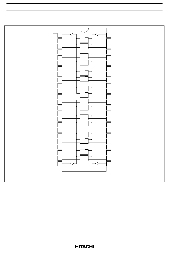
The HD74ALVCH16374 has sixteen edge trigger D type flip flops with three state outputs in a 48 pin
package. Data at the D inputs meeting set up requirements, are transferred to the Q outputs on positive
going transitions of the clock input. When the latch enable goes low, data at the D inputs will be retained at
the outputs until latch enable returns high again. When a high logic level is applied to the output control
input, all outputs go to a high impedance state, regardless of what signals are present at the other inputs and
the state of the storage elements. Low voltage and high speed operation is suitable at the battery drive
product (note type personal computer) and low power consumption extends the life of a battery for long
time operation.
Features
∑
V
CC
= 2.3 V to 3.6 V
∑
Typical V
OL
ground bounce < 0.8 V (@V
CC
= 3.3 V, Ta = 25
∞
C)
∑
Typical V
OH
undershoot > 2.0 V (@V
CC
= 3.3 V, Ta = 25
∞
C)
∑
High output current
±
24 mA (@V
CC
= 3.0 V)
∑
Bus hold on data inputs eliminates the need for external pullup / pulldown resistors.

HD74ALVCH16374
4
Absolute Maximum Ratings
Item
Symbol
Ratings
Unit
Conditions
Supply voltage range
V
CC
≠0.5 to 4.6
V
Input voltage
*1
V
I
≠0.5 to 4.6
V
Output voltage
*1, 2
V
O
≠0.5 to V
CC
+0.5
V
Input clamp current
I
IK
≠50
mA
V
I
< 0
Output clamp current
I
OK
±
50
mA
V
O
< 0 or V
O
> V
CC
Continuous output current
I
O
±
50
mA
V
O
= 0 to V
CC
V
CC
, GND current / pin
I
CC
or I
GND
±
100
mA
Maximum power dissipation
at Ta = 55
∞
C (in still air)
*3
P
T
0.85
W
TSSOP
Storage temperature
Tstg
≠65 to +150
∞
C
Notes:
Stresses beyond those listed under "absolute maximum ratings" may cause permanent damage
to the device. These are stress ratings only, and functional operation of the device at these or
any other conditions beyond those indicated under "recommended operating conditions" is not
implied. Exposure to absolute maximum rated conditions for extended periods may affect device
reliability.
1. The input and output negative voltage ratings may be exceeded if the input and output clamp
current ratings are observed.
2. This value is limited to 4.6 V maximum.
3. The maximum package power dissipation is calculated using a junction temperature of 150
∞
C
and a board trace length of 750 mils.
Recommended Operating Conditions
Item
Symbol
Ratings
Unit
Conditions
Supply voltage
V
CC
2.3 to 3.6
V
Input / Output voltage
V
I
0 to V
CC
V
OE
, CK, D
V
O
0 to V
CC
V
Q
Operating temperature
Ta
≠40 to 85
∞
C
Output current
I
OH
≠12
mA
V
CC
= 2.3 V
≠12
mA
V
CC
= 2.7 V
≠24
mA
V
CC
= 3.0 V
I
OL
12
mA
V
CC
= 2.3 V
12
mA
V
CC
= 2.7 V
24
mA
V
CC
= 3.0 V
Input rise / fall time
t
r
, t
f
10
ns/V
Note: Unused or floating control pins must be held high or low.
HD74ALVCH16374
5
Electrical Characteristics
Ta = ≠40 to 85
∞
C
Item
Symbol V
CC
(V)
*1
Min
Max
Unit
Test Conditions
Input voltage
V
IH
2.3 to 2.7
1.7
--
V
2.7 to 3.6
2.0
--
V
V
IL
2.3 to 2.7
--
0.7
V
2.7 to 3.6
--
0.8
V
Output voltage
V
OH
Min to Max V
CC
≠0.2
--
V
I
OH
= ≠100
µ
A
2.3
2.0
--
V
I
OH
= ≠6 mA, V
IH
= 1.7 V
2.3
1.7
--
V
I
OH
= ≠12 mA, V
IH
= 1.7 V
2.7
2.2
--
V
I
OH
= ≠12 mA, V
IH
= 2.0 V
3.0
2.4
--
V
I
OH
= ≠12 mA, V
IH
= 2.0 V
3.0
2.0
--
V
I
OH
= ≠24 mA, V
IH
= 2.0 V
V
OL
Min to Max --
0.2
V
I
OL
= 100
µ
A
2.3
--
0.4
V
I
OL
= 6 mA, V
IL
= 0.7 V
2.3
--
0.7
V
I
OL
= 12 mA, V
IL
= 0.7 V
2.7
--
0.4
V
I
OL
= 12 mA, V
IL
= 0.8 V
3.0
--
0.55
V
I
OL
= 24 mA, V
IL
= 0.8 V
Input current
I
IN
3.6
--
±
5.0
µ
A
V
IN
= V
CC
or GND
I
IN(hold)
2.3
45
--
µ
A
V
IN
= 0.7 V
2.3
≠45
--
µ
A
V
IN
= 1.7 V
3.0
75
--
µ
A
V
IN
= 0.8 V
3.0
≠75
--
µ
A
V
IN
= 2.0 V
3.6
--
±
500
µ
A
V
IN
= 0 to 3.6 V
Off state output current
*2
I
OZ
3.6
--
±
10
µ
A
V
OUT
= V
CC
or GND
Quiescent supply current I
CC
3.6
--
40
µ
A
V
IN
= V
CC
or GND
I
CC
3.0 to 3.6
--
750
µ
A
One input at (V
CC
≠0.6)V,
other inputs at V
CC
or GND
Notes: 1. For conditions shown as Min or Max, use the appropriate values under recommended operating
conditions.
2. For I/O ports, the parameter I
OZ
includes the input leakage current.